

Page 1
VP2611
VP2611
H.261 Encoder
Supersedes June 1996 edition, DS3487 - 4.0 DS3487 - 4.1 December 1998
FEATURES
■ Fully integrated H261 video encoder
■ Up to full CIF resolution and 30 Hz frame rates
■ Inputs YUV data in 8 x 8 sub block format
■ Outputs run length coded coefficients
■ On chip motion vector estimator with +/-7 pixel search
window
■ Addresses and control generated internally for DRAM
frame store
■ QFP package
ASSOCIATED PRODUCTS
■ VP510 Colour Space Converter
■ VP520S CIF/QCIF Converter
■ VP2612 Video Multiplexer
■ VP2614 Video Demultiplexer
■ VP2615 H.261 Decoder
DESCRIPTION
The VP2611 Video Compression Source Coder forms part
of a chip set used in video conferencing, video telephony and
multimedia applications. It produces data which conforms to
the H261 standard for video compression with rates between
64K and 2M bits per second. With a 27 MHz clock the device
will accept data produced to full CIF resolution at 30 Hz frame
rates. The pipeline latency through the device is only 3 macro
block periods.
The VP2611 contains all the elements necessary for the
compression algorithm. It incorporates a Motion Vector Estimator which performs a +/- 7 pixel search. The decision to use
inter or intra frame compression is made by the device, and the
selected data blocks are read from the frame store. New or
difference data is then passed through a Discrete Cosine
Transformer and quantized. Data from the quantizer is also
inverse quantized and passed through an Inverse Discrete
Cosine Transformer. This re-constructed data is then written
to the frame store for use in the next frame period.This frame
store is managed by an internal DRAM controller, and no
external logic is needed.
The input data must be in YUV space, and must also
conform to the six sub blocks per macro block format defined
by H261. Any conversion from RGB format is performed by
the VP510 Colour Space Converter. Any reduction in spatial
resolution, down to CIF or QCIF requirements, is done by the
VP520 Three Channel Video Filter.
The quantized data is zig-zag scanned and run length
coded before being output, together with block information
and motion vectors.
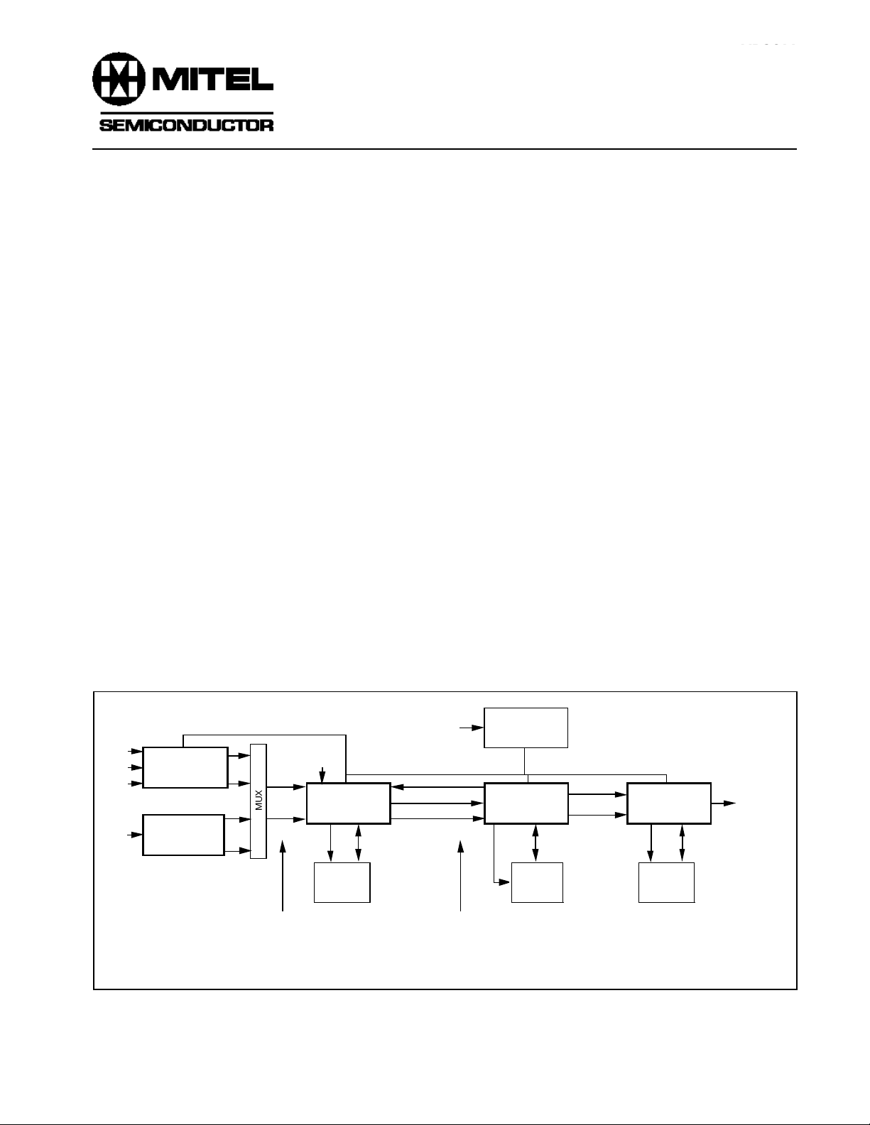
NTSC
PAL
R
COLOUR SPACE
G
B
VP510
CONVERTER
COMP VIDEO
DECODER
VIDEO
SYNC
Y
Cr/Cb
CCIR601 RESOLUTION
Y 720 X 288 Cr/Cb 360 x 288 PAL
Y 720 X 240 Cr/Cb 360 x 240
NTSC
3 CHANNEL
VIDEO FILTER
ADDR
CIF FRAME
16 X128K
VP520
STORE
Fig 1 : Typical Video Conferencing Transmission System
DATA
USER
INTERFACE
REQYUV
FRMIN
MBLK'S
CIF RESOLUTION
Y 352 X 288
Cr/Cb 176 x 144
SYSTEM
CONTROLLER
VP2611
INTEGRATED
VIDEO ENCODER
CIF FRAME
STORE
16X128K
RLC DATA
FLAGS
VP2612
VIDEO
MULTIPLEXER
TX BUFFER
32K X 8
H261
BIT
STREAM
64kb to 2Mb/s
1
Page 2
VP2611
PIN DESCRIPTIONS
YUV7:0 This input bus accepts YUV data one pixel at a
time from the preprocessor, clocked in on the
rising edge of PCLK.
PCLK This signal is used to strobe in data at the YUV
port and must be derived by dividing SYSCLK
with an integer greater than one.
FRMIN This input should be pulled high to prepare the
VP2611 to code a new frame. It must be held
high for at least one SYSCLK cycle and then
must be pulled low again before the next frame
begins. The VP2611 will respond to the rising
edge of FRMIN by asserting REQYUV
appproximately 184 SYSCLK cycles later.
REQYUV This output is pulled high to request that YUV
data be input for a new MacroBlock. It is pulled
low again 1871 SYSCLK cycles later. It remains low during Dummy MacroBlocks and
during the lay period between frames.
DBUS7:0 This output bus serves several functions as
defined by DMODE3:0. In addition to providing
the quantized coefficients and motion vectors,
it is used to output control information.
R/W1 Read/Write control for external DRAM 1.
W2 Read/Write control for external DRAM 2.
R/
N/C if 256k DRAMs.
OE1 Output Enable control for external DRAM 1
or ADR8.
OE2 Output Enable control for external DRAM 2.
N/C if 256k DRAMs.
ADR7:0 Address output for the external DRAMs.
CBUS7:0 Bi-directional data bus for use by a Microproce-
ssor. Data and insructions are clocked on and
off the chip on the rising edge of CSTR.
CSTR Data strobe for the CBUS port.
CEN An enabling signal for the CBUS port.
CADR When high, this signal defines CBUS as a data
bus, and when low as an instruction input.
SYSCLK System clock, run at 27MHz maximum. The
clock must be high for between 35% and 65%
of each clock cycle. This clock is used for all
internal operations.
DMODE3:0 Output flag port for DBUS7:0 bus. The value at
this port identifies the data type appearing on
DBUS7:0 during the same period.
DCLK This output pulses high for a minimum of 37ns
each time new data is output on DBUS or
DMODE. It can be used as an edge sensitive
strobe signal or a level sensitive "valid" signal.
SW15:0 This bidirectional port is connected to the
frame store.
RAS Row Address Strobe output for the external
DRAMs.
CAS Column Address Strobe output for the external
DRAMs.
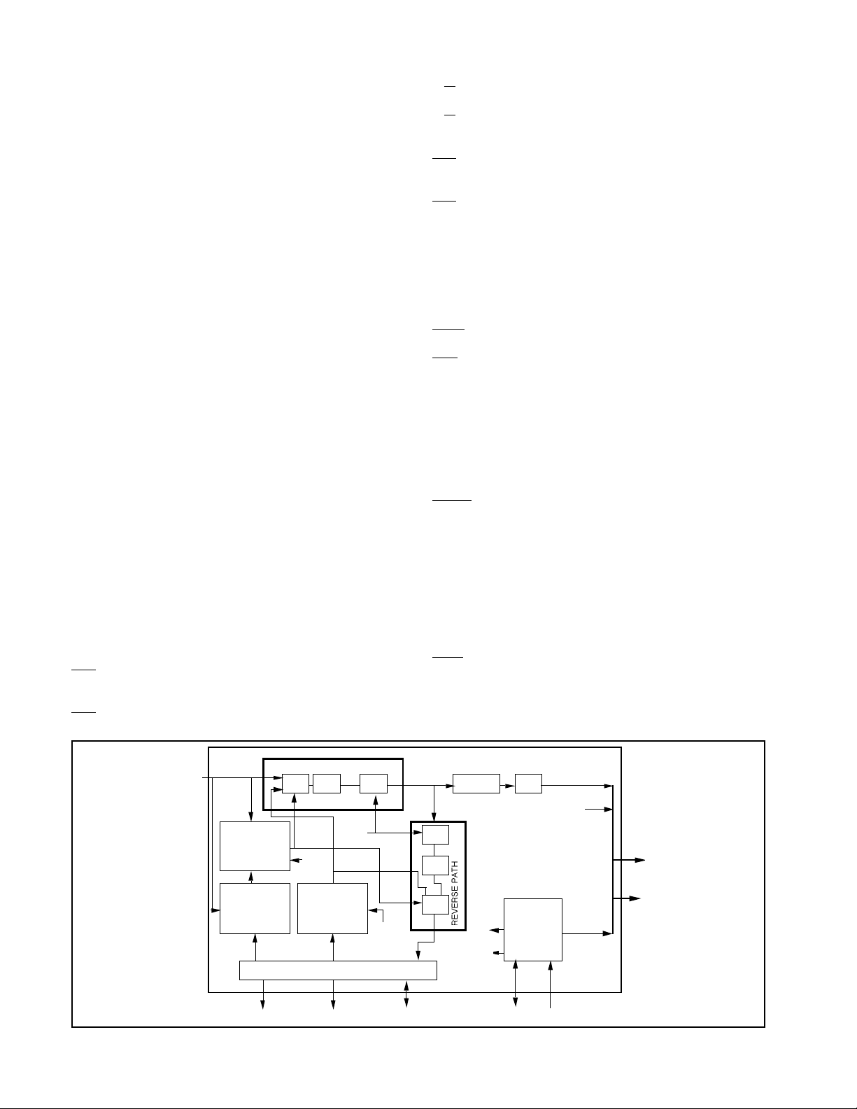
DECISION
MOTION
VECTOR
ESTIMATOR
Search
Window
FORWARD PATH
DCT
SUB
Q Step
Force
Intra
LOW
PASS
FILTER
Predicted
block
FRAME STORE INTERFACE
Q
Force
Filter
YUV
BLOCK
FORMAT
INTER/INTRA
PROCESSOR
RESET Active low power on reset which must be held
low for at least 2064 cycles.
TCK Test clock for JTAG.
TMS Test Mode Select for JTAG.
TDI Input JTAG test data.
TDO Output JTAG test data.
TRST Reset JTAG controller (active low).
NOTE:
"Barred" active low signals do not appear with a bar in the
main body of the text.
RLC
Motion Vectors
CONTROL
LOGIC
Block Info
DATA
BUS
BUS
FLAGS
IDCT
ADD
Zig Zag
IQ
Force
Intra
Force
Filter
ADDRESS
CONTROL
DATA
HOST DATA & CONTROL
Fig 2 : Simplified Block Diagram
2
Page 3
080004080
0
0
0
0
F
-
-
-
-
-
-
-
OPERATION OF MAJOR BLOCKS
Motion Vector Estimator
The motion estimator calculates the mean absolute error
( MAE ) for each possible position of the combined luminance
block in a search window from the previous frame. The
combined luminance block consists of 16 x 16 pixels, and in
the search window this is displaced between -7 to +7 vertically,
and -8 to +7 horizontally. The two lsb's of each pixel are
discarded and the MAE value is contained within 14 bits.
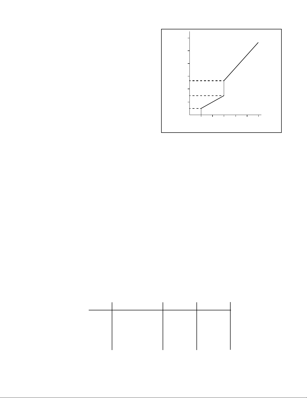
The minimum MAE value, representing the best match
between the previous and current block, is passed to the
motion compensation decision block, together with the position of this best fit in the search window. The zero displacement MAE value is also passed to this block, which then
decides whether the best fit is sufficiently better than the zero
displacement fit. It uses the characteristic shown in Figure 3,
where the 14 bit MAE is a Hex value. In the area to the right
of the line all points defined by the two MAE values will cause
motion compensation to be applied. In this case the best fit
MAE value is used by the inter/intra decision processor,
otherwise the zero displacement value is used.
Inter/Intra Decision Processor
The MAE value passed by the motion compensation
decision block is compared to the simplified variance of the
current block. This simplified variance is calculated by summing the moduli of the differences between each luminance
pixel and the mean luminance value over the whole macroblock. Eight bit pixels are used, and the variance value is
expressed in 14 bits by discarding the two lsb's from the actual
16 bit result. It can then be directly compared to the 14 bit MAE
value.
If the MAE value is below a user defined threshold inter
mode coding is always selected. The default threshold is 3, on
a scale from 0 to 255 using the 8 msb's from the 14 bit value.
Above this threshold inter mode is only selected if the variance
of the current block is greater than or equal to the MAE value
in use.
In order to avoid gradual picture degredation, every 61st
Macroblock input to the VP2611 is coded in intra mode
regardless of the above decision. As 61 is a prime number, this
will ensure that each macroblock will be transmitted in intra
mode at least once in every 61 transmissions. If FIX MACROBLOCK or SKIP PICTURE is invoked this `Force Intra'
VP2611
8
180
4
140
MC Off
100
CO
80
8
5
Minimum Mean Absolute Err or in Hex
40
4
20
4
40 80 CO 100 140 180
Zero Movement Absolute Error in Hex
Fig 3 : MC Decision Slope
counter will be disabled.
The user may overide the internal Inter/Intra decision at
any time using the CBUS control port. A user generated
forced inter mode will overide an internally generated `Force
Intra'.
Low Pass Filter
The macroblock selected from the previous frame in
motion compensated inter mode coding, will be filtered before
it is subtracted from the current block. This decision can be
overidden externally by the system controller. The Filter uses
a simple [ 1 2 1 ] characteristic in both vertical and horizontal
dimensions as specified in H.261 on the macroblock boundaries
[010] is used.
x = 1.125y
MC On
SYMBOL PARAMETER MINIMUM MAXIMUM
t RAC Access time from RAS
t CAC Access time from CAS
t RP RAS precharge time 50ns or under
t CP CAS precharge time 15ns or under
t RAS RAS pulse width 90ns or under
t CAS CAS pulse width 50ns or under
t REF Time to refresh 256 rows
N.B. All times are quoted assuming 27MHz operation. For lower clock
frequencies increase the above values proportionately.
Table 1 : External DRAM timing requirements
105ns or under
25ns or under
0.25ms or over
3
Page 4

VP2611
Frame Store Manager
The previous picture is stored in an external CIF DRAM
frame store, which is connected by a glueless interface. The
internal Frame Store Manager controls all read, write, and
refresh operations to these DRAMs. No provision is made to
allow the use of smaller DRAM's, if only QCIF operation is
required.
During the coding of each macroblock columns of the
search window are read from these DRAMs, and finally the
"best fit" macroBlock is obtained. At the completion of coding
the fully processed new macroblock is written to the DRAM's,
after it has been decoded again. In this way the frame store
maintains a bit-accurate duplicate of the image seen by the
Decoder (excepting transmission errors).
Several configurations are possible to make the required
128Kx16 store. Two 64K x 16 DRAMs could be employed; in
this case use the default 1M DRAM mode when setting up the
chip. Otherwise, a single 256K x 16 DRAM or four 256K x 4
DRAMs could be used. In these last two cases use OE1 as
ADR8, RW1 as R/W, and do not connect RW2 and OE2. Also,
use the Setup instruction at the CPORT to put the device into
4M DRAM mode.
Table 1 details the critical timing parameters which the
external DRAM must meet with SYSCLK running at 27MHz.
Note that, if used at slower speeds, the requirements on the
DRAM timing are relaxed with the exception of refresh. The
number of refresh cycles the VP2611 produces is directly
proportional to the SYSCLK frequency.
Discrete Cosine Transform
This circuit performs a Discrete Cosine Transform on each
8x8 sub block, whether in inter or intra mode. In intra mode,
eight bit pixel data is used, with a ninth implied sign bit ( all pixel
data is positive ). In inter mode the difference between the
current and best fit previous block is used. This will be a two's
complement number. Twelve bit coefficients are produced by
the DCT, and passed on to the quantizer.
Quantize
Zig Zag Scan
This is essentially an address generator which reorders
the DCT coefficients according to the standard zig-zag scan
pattern. This has the effect of concentrating the significant
coefficients at the beginning of the sub-block, improving the
efficiency of the Run Length Coder.
Run Length Coder
Each coefficient output from the zig zag scan is examined.
If it is non-zero, then the Run Length Coding circuit will pass
the coefficient magnitude to the output port along with its zero
count i.e. the number of zero magnitude coefficients preceding it within the same 8x8 sub-block.
Inverse Quantize
This circuit replicates the operation of the inverse quantizer in the decoder. It reconstructs the 12 bit DCT coefficients
from the 8 bit quantized inputs, using the 5 bit quantization
value. This is achieved using the following formulae.
If QUANT is odd :
REC = QUANT*(2*LEVEL+1) : LEVEL > 0
REC = QUANT*(2*LEVEL-1) : LEVEL < 0
If QUANT is even :
REC = QUANT*(2*LEVEL+1)-1 : LEVEL > 0
REC = QUANT*(2*LEVEL-1)+1 : LEVEL < 0
For Intra Coded DC Coefficients :
REC = 8*LEVEL
except if LEVEL=255 when REC=1024
If LEVEL=0 then REC=0 in all cases.
The reconstructed values (REC) are passed through a
Clipping Circuit in case of arithmetic overflow.
Thus, the Inverse Quantizer restores the DCT coefficients
to their original value but with quantisation error.
This section quantizes the results of the DCT by dividing
the 12 bit output from the DCT with a host supplied value. The
5 bit quantization value supplied corresponds to division of the
12 bit coefficients ( range ± 2048 ) by values from 2 to 62, but
in steps of 2. This variable quantization strategy allows the
volume of data generated by the encoder to be adjusted
dynamically, depending on the fullness of the transmission
buffer. For H.261 applications it uses the quantisation value
provided at the control port during the previous Macroblock
period (or at some earlier time). An option is provided which
allows two quantisation values to be used, one for use with
inter coded macroblocks, and the other for use with intra
coded macroblocks.
As specified in H.261, the DC coefficient of an Intra coded
Block is treated differently and the 12 bit value is always
divided by 8.
When the quantization value is small, and the DCT coefficient is large, there is a danger of overflow in the eight bit
output. To avoid this a clipping circuit is included at the output
of the quantizer, which saturates at the maximum values.
4
Inverse DCT
This circuit replicates the operation of the Inverse Cosine
Transform in the Decoder, and outputs 9 bit signed pixel data
(intra mode) or pixel difference data (inter mode). The IDCT
fully meets the CCITT specification.
Reconstruction Adder
In Inter Mode, the IDCT data is added to the best fit block
from the previous frame store. In Intra mode, the IDCT data is
simply added to zero. After the adder, the sign bit is removed
from the result to give 8 bit pixels. Clipping circuits ensure that
any pixels with values exceeding 255 are clipped to 255, and
any with negative values are clipped to zero (such values are
possible due to quantization noise).
Page 5
VP2611
Y
K
K
2064 cycles
YUV Input
Frame Store Read
Control Decisions
Frame Store Write
DBUS Output
MB1 MB2 MB3 MB4
DUMMY MB1 MB2 MB3
DUMMY MB1 MB2 MB3
DUMMY DUMMY DUMMY MB1
DUMMY DUMMY DUMMY MB1
Fig 4: MacroBlock Pipelining
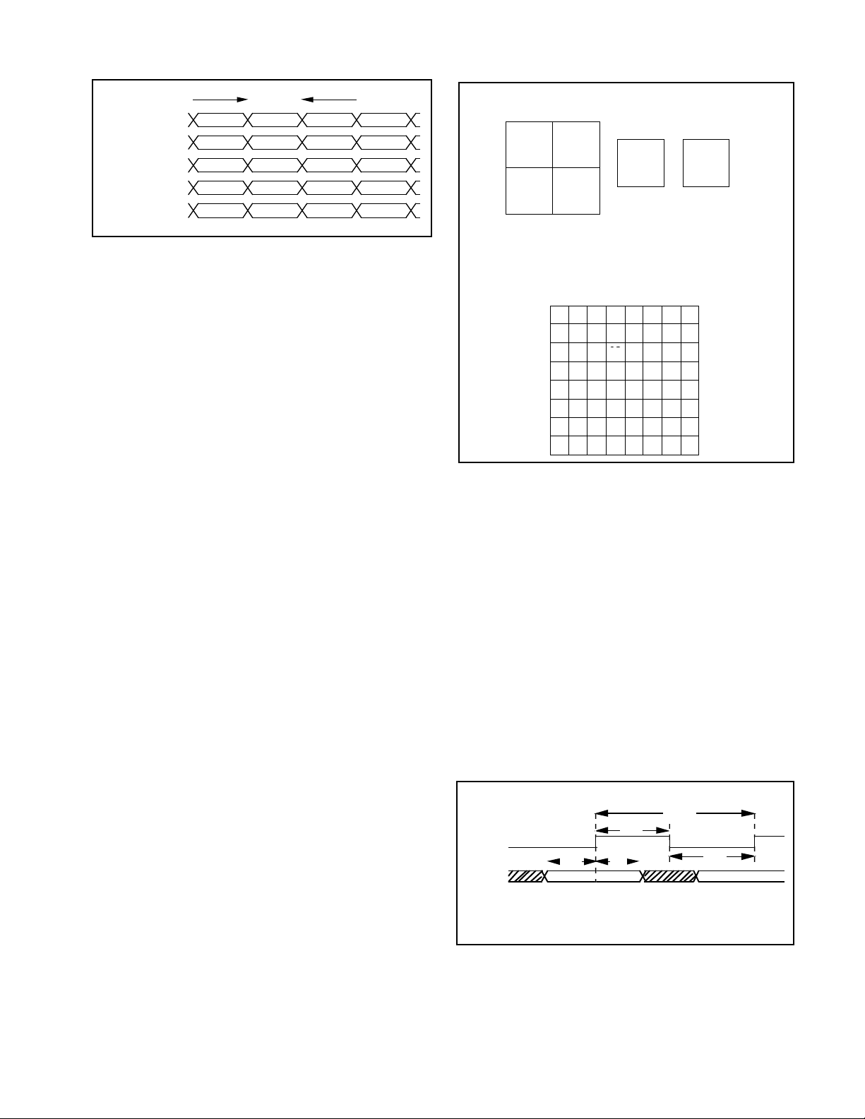
OPERATION OF INTERFACES
Macroblock Delays
The VP2611 has a three macroblock pipeline delay between pixel inputs and run length coded outputs. This is
illustrated in Figure 4. Whilst the second macroblock is being
input, the best fit macroblock from the previous frame is being
identified and then read from the frame store. At this time any
Control Decisions which are to effect the first macroblock must
be supplied by the host controller. The run length coded
outputs for the first macroblock are not available until the
fourth macroblock is supplied at the input pins.
YUV Input Port
The YUV port accepts pixel data from the preprocessor in
block format as illustrated in Figure 5. Within a complete
system the VP2611 is always the master device, and must be
supplied with macroblock data when it makes a demand. The
order in which pixels are supplied is pre-determined, and must
be strictly maintained. There are 64 pixels per sub-block and
4 luminance and 2 chrominance sub-blocks per macroblock.
The macroblocks themselves are divided into groups of blocks
( GOB's ), and the sequence specified in H.261 must also be
maintained. Note that, since the chrominance resolution is half
the luminance resolution both vertically and horizontally, then
the two chrominance blocks cover the same picture area as
the four luminance blocks.
The pre-processor producing macroblock data must produce a frame start signal ( FRMIN ) when it has a complete
frame of data available. This resets the input controller within
the VP2611, which will then generate sequential GOB and
macroblock numbers for the coded outputs referenced to this
input.
FRMIN must go high for at least one system clock period,
and must go low before the next frame is available. The
VP2611 responds to FRMIN with a request for macroblock
data ( REQYUV ), which occurs approximately 184 SYSCLK
periods after FRMIN. It must then receive a complete macroblock within 1871 SYSCLK periods, and at the end of this time
REQYUV will go inactive. The VP2611 must be provided with
a PCLK signal to strobe in the data. This must be derived from
SYSCLK, and must only be present when there is valid data
at the input. Data must meet the set up and hold times with
respect to PCLK as specified in Figure 6.
The maximum peak rate for PCLK is the SYSCLK rate
divided by two, but since there are 384 bytes per macroblock
SUBBLOCK ORDER WITHIN MACROBLOC
1 2
5
3 4
PIXEL ORDER WITHIN SUBBLOC
00 01 02 03 04 05 06 07
08 09 10 11 12 13 14 15
16 17 18 03 20 21 22 23
24 25 26 27 28 29 30 31
32 33 34 35 36 37 38 39
40 41 42 43 44 45 46 47
48 49 50 51 52 53 54 55
56 57 58 59 60 61 62 63
U
19
6
V
Fig 5 : Ordering of Pixels
then theoretically the average rate need only be 384/1871
times the SYSCLK rate. Note that PCLK must always be
obtained by dividing SYSCLK by an integer greater than one.
When the VP520 CIF/QCIF Converter is supplying the VP2611
with data, it provides a peak PCLK rate equivalent to SYSCLK
divided by two, and an average rate of SYSCLK divided by
four.
The mimimum gap between REQYUV going active is
2064 SYSCLK periods. In full CIF mode "dummy" macroblocks are internally inserted between rows, in order to give the
chip sufficient time to load a new search window. No new YUV
data must be loaded during these dummy macroblocks, and
REQYUV will remain inactive. No dummy macroblocks are
required in QCIF mode. With a 27MHz SYSCLK all macroblocks will be coded in less than a 30Hz frame rate period, and
there will be a period of inactivity before FRMIN goes active
again. During this period the output bus will remain static at all
ones, and no output strobe ( DCLK ) will be produced.
SCLK/2
20ns
PCLK
YUV7:0
20ns
10ns
N.B. All timings given are MINIMUM values.
0ns
Fig 6 : Timing at YUV Port
5
Page 6

VP2611
DBUS Output Port
The DBUS port is used to pass data and control information directly to the VP2612 Video Multiplexer. The type of data
on the output pins is identified by the DMODE 3:0 outputs,
using the codes shown in Table 2. An output strobe is also
produced ( DCLK ) which always goes high one system clock
period after the data defined by DMODE 3:0 becomes valid.
This edge is used to strobe the data into the Video Multiplexer,
and thus the data set up time is always one SYSCLK period
minus differential output delays.
The number of SYSCLK periods during which data remains valid is dependent on the type of data, and DCLK
remains high for this same period. It goes low as the result of
the same SYSCLK rising edge which produces a change in
DMODE 3:0. The output delays with respect to SYSCLK are
illustrated in Figure 8, and Figure 9 shows a typical output
sequence during which DCLK remains high for several cycles
as the sub-block number ( code 7 ) is produced. During a Wait
State
( code 15 ) no DCLK transitions are produced. The actual
sequence of output events which occur for each macroblock,
and the duration of each event, are illustrated in Figure 7.
The output events are defined in more detail below;
Control Decisions : This byte shows which control decisions
have been taken for the forthcoming macroblock. DBUS0
will be high if a Fixed Macroblock (FIX MB) was enforced
i.e. no new data will be transmitted this macroblock.
DBUS1 indicates whether Inter (high) or Intra (low) coding
was used for the macroblock. DBUS2 will be high if the
macroblock was filtered, and DBUS3 will be high if motion
compensation was used. DBUS5 will be high if the current
frame is being coded in FAST UPDATE mode. In this
mode the complete frame will be intra coded. DBUS6 will
be high if the current frame is a SKIP FRAME i.e. not being
coded - so no coefficients will be transmitted. DBUS4 and
DBUS7 are not used.
START MB
WAIT
IS IT
A DUMMY
BLOCK?
no
CONTROL (2 cycles)
GOB (2 cycles)
MB
CBP (2 cycles)
QUANT (2 cycles)
HORZ MV (2 cycles)
VERT MV
ARE
ANY BLOCKS
CODED?
yes
WAIT (32 cycles)
SUB BLK NO (15 cycles)
RUN LENGTH
MAGNITUDE
(2 cycles)
yes
(2 cycles)
(2 cycles)
no
(2 cycles)
(2 cycles)
WAIT
(1 cycle)
DMODE3:0 FUNCTION
0000
0001
0010
0011
0100
0101
0110
0111
1000
1001
1010
1011
1100
1101
1110
1111
6
Table 2 : DBUS Functions
GOB Number
MB Number
Control Decisions
Quant Value
Horizontal MV
Vertical MV
Coded Blk Pattern
Sub-Block No
Zero Run Count
RLC Coefficient
Not used
Not used
Not used
Not used
Not used
Wait State
ALL COEFFS
no
yes
no
ALL BLOCKS
yes
END MB
ARE
O/P?
WAIT
ARE
O/P?
WAIT
(wait variable time to make total
time since start of sub-block up
to 335 cycles)
(variable cycles)
Fig 7 : DBUS Port Flow Chart
Page 7

VP2611
N
r
r
SCLK
DCLK
DATA FROM
VP2611
DMODE
3:0
20ns max
25ns max
20ns max
DATA VALID
DATA VALID
Fig 8: Timing diagram
GOB Number : At the start of each new macroblock, the
current GOB Number is output on DBUS3:0. (DBUS3 is
MSB).
MB Number : After the GOB Number, the macroblock
Number is output on DBUS5:0 (DBUS5 is MSB).
Coded Block Pattern : This byte contains a 6 bit linear code
that indicates which of the sub-blocks actually contain
coded data. DBUS6 will be high if sub-block 1 contains
coded data, through to DBUS 1 being high if sub-block 6
contains coded data. DBUS7 and DBUS0 are not used.
Note that if the macro block is not motion compensated
and the coded block pattern is all zero's, the fixed macro
block bit will be set in the control decisions byte.
Quant Value :The quantisation value used in processing the
current macroblock is output on DBUS4:0 (DBUS4 is
MSB). This represents an actual quantisation level between 2 and 62, in steps of 2 and as defined in H.261.
Horizontal MV : If motion compensation is used, the horizontal
component of the motion vector will be output on DBUS4:0
(DBUS4 is MSB). This 5 bit value represents a two's
complement number in the range +/-15
(although only vectors in the range -8 to +7 are currently
possible with the VP2611).
Vertical MV : If motion compensation is used, the vertical
component of the motion vector will be output on DBUS4:0
(DBUS4 is MSB). This 5 bit value represents a two's
complement number in the range ±15 ( although only
vectors in the range ±7 are currently possible with the
VP2611).
CBUS3:0 INSTRUCTIO
0000
0001
0010
0011
0100
0101
0110
0111
1000
1001
1010
1011
1100
1101
1110
1111
Input VAR Threshold
Reserved
Input Inter Quantiser
Input Intra Quantiser
Input Setup Data
Input Control Functions
Reserved
Reserved
Output GOB Numbe
Output MB Numbe
Reserved
Output Control Decisions
Output Setup Data
Reserved
Reserved
Overide internal clock doubler
Table 3 : CBUS Instruction Codes
Sub-block Number : An identifier for the run length coded
coefficients which are about to be made available. DBUS
2:0 contain the coded sub-block number from 1 to 6. All
zero sub-blocks will not be produced at the outputs, and
their corresponding numbers will not appear.
Zero Run Count : The number of zero valued coefficents
preceding the next non zero coefficient is available on
DBUS5:0 (DBUS5 is MSB). Normally, DBUS7:6 are low,
except to signify the end of a Sub-block, when they will
both be high. Zero Run Count is always followed by a
coefficient, even at the end of a sub-block.
RLC Coefficient : This byte contains the 8 bit coefficient value.
It will always be a non-zero value, except when the
previous Zero Run Count signalled the end of sub-Block.
A zero value is then possible since, as stated above, the
run count is always followed by a coefficient byte, which
may be zero if the last coefficient is zero.
Wait State : This indicates that no valid data is being output
from the DBUS port during this cycle. No DCLK is produced for this state.
Pins which are "not used" for certain functions will be
forced low.
This diagram shows a typical Sub-block being output from the VP2611.
DCLK
DMODE
DBUS
15
Both msb's are high showing end of block.
15
1515 7 8 9 8 9 8 9
XX
XX 2 0 4 1 -2 252 0
Fig 9: DBUS Timing
7
Page 8

VP2611
GOOCUS
CBUS Control Port
The CBUS control port is used to input control and setup
information and also to output status information. In order to
save on pin count, a microprocessor driving this port is
required to execute two I/O instructions in order to transfer a
single byte of information to or from the device. The first
transfer is always a write operation, with a low level on the
single address line which is used by the interface. Data on the
bus then defines the instructions listed in Table 3. The second
transfer can be a read or write operation as necessary, but the
address line must then be high with the set up time given in
Figure 10.
In addition to the single addresss line (CADR), data
transfers use a control strobe (CSTR) which is only effective
when a chip enable is present (CEN). Detailed timing informa-
WRITING DATA FROM THE CBUS:
This diagram shows a typical instruction and associated data field being written to the device.
10ns
CEN
CADR
CSTR
CBUS
I/P
20ns
20ns
20ns
20ns
20ns
20ns
20ns
20ns
INSTRUCTION
10ns
10ns
10ns
10ns
10ns
20ns
tion is given in Figure 10, and when writing data or instructions
to the VP2615 the set up and hold times which are referenced
to the rising edge of CSTR must be maintained.
When a write instruction has been defined CADR should
be pulled high, valid data presented to CBUS7:0 and then
strobed in using CSTR. Other system I/O transfers can occur
between defining a write operation and supplying the data to
be written, assuming CEN is not active during those other
transfers. If CSTR does not go active because of I/O transfers
to other devices, then CEN can remain active low between the
instruction and data.
When a read instruction has been specified the requested
data will then be output on CBUS7:0 after the access time
specified from CEN going low, assuming that CADR was
already high. Otherwise the data will become valid after the
access time specified from CADR going high after CEN was
10ns
20ns
20ns
20ns
20ns
DATA IN
10ns
10ns
READING INFORMATION ON CBUS :
This diagram shows a typical instruction and associated data field being read from the device.
CEN
CADR
CSTR
CBUS
If Th is less than 5 ns then CBUS may be driven by the VP2615until CEN going high eventually turns off
the drivers. It will not prevent correct data being read when CEN again goes active
N.B. All timings shown are minimum values except those marked * which are maximums.
20ns
10ns
Th
20ns
20ns
20ns
INSTRUCTION
10ns
10ns
20ns
50ns
Fig 10 : Use of the Control Port
10ns
20ns
20ns
20ns
20ns
*
*
DATA OUT
10ns
10ns
20ns
*
8
Page 9

VP2611
low. Note that in the data read phase CADR must always go
high before CSTR goes high, with the set up time specified.
When CEN goes high, or CADR goes low, the CBUS will go
high impedance after the delay specified.
Note that the access times under the conditions given
above are only true when the gap between CSTR going high
in the instruction phase, and CEN going low in the data phase,
is greater than the minimum specified in figure 10.
Only the four LSBs, CBUS3:0, are used when writing
instructions to the VP2611. The remaining bits, CBUS7:4,
should be pulled low while the instruction is strobed into the
VP2611.
The instructions listed in Table 3 are described below in
greater detail;
Input VAR Threshold: VAR is the difference between the best
fit MAE value and the variance of the current macroblock.
The VAR Threshold is the best fit MAE value below which
Inter Frame Prediction is always used, no matter what the
variance of the current block. Above this threshold inter
mode coding is only used if the best fit value is less than
the current block variance. The default value is 3, within a
range of 0 - 255 using the eight most significant bits of the
14 bit value. In normal operation values below 15 should
be used.
Decision circuitry will be overidden according to CBUS1;
if CBUS1 is HIGH then all subsequent macroblocks will be
intra coded, if it is LOW they will be inter coded. When
CBUS2 is HIGH the on-board Filter Decision circuitry is
overidden according to CBUS3; if CBUS3 is HIGH then the
filter will be forced on, if it is LOW the filter will be forced off.
If CBUS4 is HIGH then FIX MB will be implemented, and
no new data from the current macroblock will be coded. A
two macroblock delay exists between defining the Force
Inter/Intra, Force Filter or FIX MB decisions through the
control bus and data being affected at the outputs. These
decisions will stand for all subsequent macroblocks until
they are again changed. If CBUS5 is HIGH a FAST
UPDATE will be performed on the next frame and all
blocks will be coded in intra mode. If CBUS6 is HIGH then
the next frame will not be transmitted ( SKIP FRAME ).
Note that these two global frame bits do not take effect until
the start of the next frame, and stay in effect for all frames
until they are removed. If CBUS7 is HIGH, then the onboard Force Update Controller will be overidden, and the
user will have to enforce their own Force Update policy
using the Force Intra command. RESET will cause the
options to default to those defined by the LOW state. Note
that SKIP FRAME has priority over any other bits and that
FIXMB has priority over all bits bar SKIP FRAME. See
note below.
Input Inter Quantiser: Coefficents of inter coded macroblocks
will be quantized using the value on CBUS4:0 following
this instruction. Internally this represents a 6 bit number
with the lsb always zero, giving a value between 0 and 62
in steps of two. Where only one quantization value is to be
used for both inter and intra cases, this instruction should
be used. On reset the value will default to the maximum
allowed. See note below.
Input Intra Quantiser: This instruction is similar to the above,
except that it defines the quantization level for intra mode
coding when it is to be different to that of inter mode coding.
See note below.
Input Setup Data: This instruction allows several user defined
options to be specified, using individual bits in the following
data word. If CBUS0 is LOW the device will work in full CIF
mode , if HIGH it uses the QCIF mode. If CBUS3 is HIGH
both inter and intra quantization values will be used,
otherwise a common value will be used. If CBUS5 is high
then the motion compensation circuits will be disabled. If
CBUS6 is high, then the device will be configured to use
256K x 16 or 256K x 4 DRAM's, otherwise it will assume the
use of two 64K x 16 DRAM's. The default conditions after
RESET are those selected by the Low level. CBUS1,
CBUS2, CBUS4 and CBUS7 are not used but must be low
during the definition phase. This instruction may be used
any time after RESET has gone high, but the video input
bus must not be active. If a subsequent mode change
between CIF and QCIF is made then a further RESET is
needed.
Input Control Functions: This instruction specifies several
control options using individual bits in the following data
word. If CBUS0 is HIGH then the on board Inter/Intra
Output GOB Number: This instruction will output the GOB
Number on CBUS3:0, for the data currently being output
on DBUS. CBUS7:4 are not used (always low).
Output MB Number: This instruction will output the macrob-
lock number on CBUS5:0, for the data currently being
output on DBUS. If CBUS6 is low it indicates that the
macroblock number has just changed, or is about to
change. New Quantization Value or Control Function
words should not be written at this time since it is uncertain
which macroblock they will effect. CBUS7 is not used
(always low).
Output Control Decisions: This instruction will output the
details of several control decisions on the CBUS. CBUS0
shows whether the MacroBlock currently being output on
DBUS was inter or intra coded (0=Intra). CBUS1 shows
whether motion compensation was used (1=MC used).
CBUS3 shows whether the macroblock was passed
through the loop filter or not (1=Filtered). CBUS4 will be
high if the FIX MB instruction was enforced. CBUS5 will be
high if FAST UPDATE is currently being undertaken.
CBUS6 will be high if SKIP FRAME is in force. CBUS2 and
CBUS7 are not used.
Output Setup Data: This instruction allows the user to verify
the internal setup previously selected. The bits have the
same significance as in the Input Setup Data Instruction.
Note
For definitive operation the output MB number should be
read first, and these bytes only changed if CBUS b is high.
9
Page 10

VP2611
g
Initialising the VP2611
On power-up, RESET should be low and must remain low
for at least 2064 cycles of SYSCLK. After RESET is pulled
high, FRMIN may be activated to start the first frame. Before
activating FRMIN for the first time, it is advisable to use the
CBUS to implement a FAST UPDATE for the first frame (i.e.
all blocks Intra coded).
JTAG Test Interface
The VP2611 includes a test interface consisting of a
boundary scan loop of test registers placed between the pads
and the core of the chip. The control of this loop is fully JTAG/
IEEE 1149-1 1990 compatible. Please refer to this document
for a full description of the standard.
The interface has five dedicated pins: TMS, TDI, TDO,
TCK and TRST. The TRST pin is an independent reset for the
interface controller and should be pulsed low, soon after
power up; if the JTAG interface is not to be used it can be tied
low permanently. The TDI pin is the input for shifting in serial
instruction and test data; TDO the output for test data. The
TCK pin is the independent clock for the test interface and
registers, and TMS the mode select signal.
TDI and TMS are clocked in on the rising edge of TCK, and
all output transitions on TDO happen on its falling edge.
Instructions are clocked into the 8 bit instruction register
(no parity bit) and the following are available.
Instruction Register Name
( MSB first )
11111111 BYPASS
00000000 EXTEST (No inversion)
01000000 INTEST
XX001011 SAMPLE/PRELOAD
Timing details for the JTAG control signals are shown in fig
11.The maximum TCK frequency is 5 MHz.
The test registers, their positions in the boundary loop and
the corresponding i/o pad are detailed in Table 4. Note that the
three state control signals also have test registers associated
with them which are labelled as TRI in Table 4. DHz is an
output enable for all signals to the DRAM. The order given in
Table 4 determines the serial data stream needed for JTAG
testing.
TCK
Signal
TCK
Signal
TMS toTCK timing
TDI to TCK timing
Chip i/p to TCK timin
TCK to TDO timing
Fig 11 : JTAG Interface timing
Tsu
Thd
Tprop
Tsu Thd Tprop
15
15
15
5
5
5
20
Pad Type Reg No Pad Type Reg No Pad Type Reg No
RESET
CADR
CSTR IN
CEN IN
CBUS0 OP
CBUS1
CBUS2
CBUS3
CBUS4
CBUS5 OP
CBUS6
CBUS7
DCLK OP
DMODE0 OP
DMODE1 OP
DMODE2
DMODE3
DBUS0 OP
DBUS1 OP
DBUS2 OP
DBUS3 OP
DBUS4
IN 93
IN
TRI
IN
OP
IN
OP
IN
OP
IN
OP
IN
IN
OP
IN
OP
IN
OP
OP
OP
92
91
90
89
88
87
86
85
84
83
82
81
80
79
78
77
76
75
74
73
72
71
70
69
68
67
66
65
64
63
DBUS5 OP
DBUS6 OP
DBUS7 OP
SW15 OP
SW14 OP
SW13 OP
SW12 OP
SW11 OP
SW10 OP
SW9 OP
SW8 OP
SW7
SW6 OP
SW5 OP
SW4 OP
TRI
IN
IN
IN
IN
IN
IN
IN
IN
OP
IN
IN
IN
IN
SW3 OP
IN
SW2 OP
62
61
60
59
58
57
56
55
54
53
52
51
50
49
48
47
46
45
44
43
42
41
40
39
38
37
36
35
34
33
32
IN
SW1 OP
SW0 OP
REQYUV
IN
IN
DHZ TRI
RAS OP
CAS OP
RW1 OP
RW2 OP
OE1 OP
OE2 OP
ADR0 OP
ADR1 OP
ADR2 OP
ADR3 OP
ADR4 OP
ADR5 OP
ADR6 OP
ADR7 OP
PCLK IN
YUV7
YUV6 IN
YUV5 IN
YUV4 IN
YUV3 IN
YUV2 IN
SYSCLK IN
FRMIN
IN
YUV1 IN
YUV0 IN
IN
OP
31
30
29
28
27
26
25
24
23
22
21
20
19
18
17
16
15
14
13
12
11
10
9
8
7
6
5
4
IN
3
2
1
0
10
Table 4 Pin and JTAG test registers
Page 11

ABSOLUTE MAXIMUM RATINGS [See Notes]
Supply voltage VDD -0.5V to 7.0V
Input voltage V
Output voltage V
Clamp diode current per pin I
Static discharge voltage (HBM) 500V
Storage temperature T
Ambient temperature with power applied T
IN
OUT
(see note 2) 18mA
K
S
Junction temperature 125°C
Package power dissipation 3000mW
NOTES ON MAXIMUM RATINGS
1. Exceeding these ratings may cause permanent damage.
Functional operation under these conditions is not implied.
2. Maximum dissipation for 1 second should not be exceeded,
only one output to be tested at any one time.
3. Exposure to absolute maximum ratings for extended
periods may affect device reliablity.
4. Current is defined as negative into the device.
-0.5V to VDD+ 0.5V
-0.5V to VDD + 0.5V
-55°C to 150°C
AMB
0°C to 70°C
VP2611
STATIC ELECTRICAL CHARACTERISTICS Operating Conditions (unless otherwise stated)
Tamb = 0 C to +70°C VDD = 5.0v ± 5%
Characteristic
Output high voltage
Output low voltage
Input high voltage
Input low voltage
Input leakage current
Input capacitance
Output leakage current
Output S/C current
Symbol
V
OH
V
OL
V
IH
V
IL
I
IN
C
IN
I
OZ
I
SC
Min.
2.4
-
2.0
-
-10
-50
10
Value
Typ.
10
Max.
-
0.4
-
0.8
+10
+50
300
Units
V
V
V
V
µA
pF
µA
mA
Conditions
I
= 4mA
OH
I
= -4mA
OL
V
-1V for SYSCLK and PCLK
DD
GND < V
GND < V
VDD = Max
IN
OUT
< V
< V
DD
DD
ORDERING INFORMATION
VP2611 CG GH1R (Commercial - Plastic QFP power package)
11
Page 12

VP2611
Pin
1
2
3
4
5
6
7
8
9
10
11
12
13
14
15
16
17
18
19
20
21
22
23
24
25
26
27
28
29
30
31
32
33
34
35
36
37
38
39
40
41
42
43
Function
SW3
NC
SW4
SW5
GND
VDD
SW6
SW7
NC
SW8
SW9
SW10
SW11
NC
GND
SW12
NC
VDD
SW13
SW14
NC
SW15
DBUS7
DBUS6
NC
DBUS5
GND
VDD
DBUS4
DBUS3
NC
DBUS2
NC
NC
DBUS1
DBUS0
DMODE3
NC
GND
VDD
DMODE2
DMODE1
DMODE0
Pin
44
45
46
47
48
49
50
51
52
53
54
55
56
57
58
59
60
61
62
63
64
65
66
67
68
69
70
71
72
73
74
75
76
77
78
79
80
81
82
83
84
85
86
Function
DCLK
NC
CBUS7
VDD
CBUS6
GND
VDD
CBUS5
GND
CBUS4
CBUS3
CBUS2
CBUS1
NC
GND
VDD
CBUS0
TRST
CEN
NC
NC
CSTR
NC
CADR
RESET
VDD
GND
TCK
TMS
TDI
NC
TDO
(CLK54)
REQYUV
FRMIN
VDD
NC
SYSCLK
GND
NC
YUV0
YUV1
YUV2
Pin
87
88
89
90
91
92
93
94
95
96
97
98
99
100
101
102
103
104
105
106
107
108
109
110
111
112
113
114
115
116
117
118
119
120
121
122
123
124
125
126
127
128
Function
YUV3
NC
YUV4
YUV5
VDD
GND
YUV6
YUV7
NC
PCLK
NC
NC
ADR7
ADR6
ADR5
VDD
GND
NC
ADR4
ADR3
ADR2
ADR1
GND
ADR0
VDD
GND
NC
OE2
OE1
VDD
RW2
RW1
CAS
RAS
VDD
GND
NC
SW0
SW1
SW2
NC
NC
12
Pin out table for GH128 PQFP package
Page 13

Page 14

http://www.mitelsemi.com
World Headquarters - Canada
Tel: +1 (613) 592 2122
Fax: +1 (613) 592 6909
North America Asia/Pacific Europe, Middle East,
Tel: +1 (770) 486 0194 Tel: +65 333 6193 and Africa (EMEA)
Fax: +1 (770) 631 8213 Fax: +65 333 6192 Tel: +44 (0) 1793 518528
Fax: +44 (0) 1793 518581
Information relating to products and services furnished herein by Mitel Corporation or its subsidiaries (collectively “Mitel”) is believed to be reliable. However, Mitel assumes no
liability for errors that may appear in this publication, or for liability otherwise arising from the application or use of any such information, product or service or for any infringement of
patents or other intellectual property rights owned by third parties which may result from such application or use. Neither the supply of such information or purchase of product or
service conveys any license, either express or implied, under patents or other intellectual property rights owned by Mitel or licensed from third parties by Mitel, whatsoever.
Purchasers of products are also hereby notified that the use of product in certain ways or in combination with Mitel, or non-Mitel furnished goods or services may infringe patents or
other intellectual property rights owned by Mitel.
This publication is issued to provide information only and (unless agreed by Mitel in writing) may not be used, applied or reproduced for any purpose nor form part of any order or
contract nor to be regarded as a representation relating to the products or services concerned. The products, their specifications, services and other information appearing in this
publication are subject to change by Mitel without notice. No warranty or guarantee express or implied is made regarding the capability, performance or suitability of any product or
service. Information concerning possible methods of use is provided as a guide only and does not constitute any guarantee that such methods of use will be satisfactory in a specific
piece of equipment. It is the user’s responsibility to fully determine the performance and suitability of any equipment using such information and to ensure that any publication or
data used is up to date and has not been superseded. Manufacturing does not necessarily include testing of all functions or parameters. These products are not suitable for use in
any medical products whose failure to perform may result in significant injury or death to the user. All products and materials are sold and services provided subject to Mitel’s
conditions of sale which are available on request.
M Mitel (design) and ST-BUS are registered trademarks of MITEL Corporation
Mitel Semiconductor is an ISO 9001 Registered Company
Copyright 1999 MITEL Corporation
All Rights Reserved
Printed in CANADA
TECHNICAL DOCUMENTATION - NOT FOR RESALE
 Loading...