

Datasheet VNW35NV04, VNV35NV04, VNP35NV04, VNB35NV04 Datasheet (SGS Thomson Microelectronics)
Page 1

®
VNB35NV04 / VNP35NV04
/ VNV35NV04 / VNW35NV04
“OMNIFET II”:
FULLY AUTOPROTECTED POW ER M OSFET
TYPE R
DS(on)
I
lim
V
clamp
VNB35NV04
VNP35NV04
VNV35NV04
10 mΩ (*) 30 A 40 V
VNW35NV04
(*) For PowerSO-10 only
n
LINEAR CURRENT LIMITATION
n
THERMAL SHUT DOWN
n
SHORT CIRCUIT PROTECTION
n
INTEGRATED CLAMP
n
LOW CURRENT DRAWN FRO M INPUT PIN
n
DIAGNOSTIC FEEDBACK THROUGH INPUT
PIN
n
ESD PROTECTION
n
DIRECT ACCESS TO THE GATE OF THE
POWER MOSFET (ANALOG DRIVING)
n
COMPATIBLE WITH STANDARD POWER
MOSFET
DESCRIPTION
The VNB35NV04, VNP35NV04, VNV35NV04,
VNW35NV04 are mono lithic devices desig ned in
STMicroelectronics VIPower M0-3 Technology,
BLOCK DIAGRAM
10
D2PAK
TO-220
3
1
PowerSO-10
3
2
1
TO-247
1
™
3
2
1
ORDER CODES:
2
PAK
D
VNB35NV04
TO-220 VNP35NV04
PowerSO-10
™
VNV35NV04
TO-247 VNW35NV04
intended for replacement of standard Power
MOSFETS from DC up to 25KHz applications.
Built in thermal shutdown, l inear curre nt limitation
and overvoltage clamp protect the chip in harsh
environments. F ault f eedba c k can b e detected by
monitoring the voltage at the input pin.
DRAIN
2
Overvoltage
Clamp
INPUT
1
Gate
Control
Linear
Over
T emperature
Current
Limiter
3
SOURCE
FC01000
July 2003 1/19
Page 2
VNB35NV04 / VNP35NV04 / VNV35NV04 / VNW35NV04
ABSOLUTE MAXIMUM RATI NG
Symbol Parameter
V
R
IN MIN
V
V
T
V
ESD1
ESD2
P
Drain-source Voltage (VIN=0V) Internally Clamped V
DS
Input Voltage Internally Clamped V
IN
Input Current +/-20 mA
I
IN
Minim um Input Series Impe dance 4.7 Ω
Drain Current Internally Limited A
I
D
Reverse DC Output Current -30 A
I
R
Electrostatic Di scharge (R=1 . 5 K Ω, C=100pF) 4000 V
Electrostatic Discharge on output pin only
(R=330Ω, C=150pF)
Total Dissipation at Tc=25°C 125 125 125 208 W
tot
Opera ting Junct ion Temp erature Internal ly limi ted °C
T
j
Case Operating Temperature Internally limited °C
T
c
Storage Temper ature -55 to 150 °C
stg
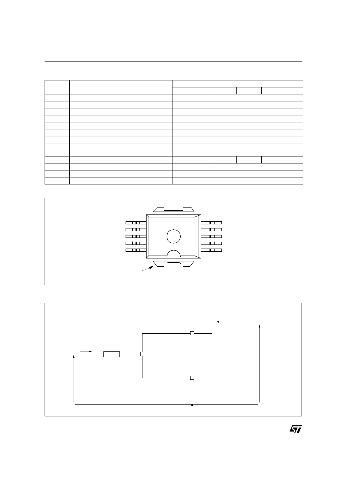
CONNECTION DIAGRAM (TO P VI EW)
PowerSO-10
™ D
Value Unit
2
PAK TO-220 TO-247
16500 V
INPUT
INPUT
INPUT
INPUT
INPUT
6
7
8
9
10
11
DRAIN
(*) For the pins configuration related to TO-220, TO-247, D2PAK, see outlines at page 1.
CURRENT AND VOLTAGE CONVENTION S
R
I
IN
IN
INPUT
5
4
3
2
1
DRAIN
SOURCE
SOURCE
SOURCE
N.C.
SOURCE
SOURCE
I
D
V
DS
2/19
V
IN
Page 3
VNB35NV04 / VNP35NV04 / VNV35NV04 / VNW35NV04
THERMAL DATA
Symbol Parameter
R
thj-case
R
thj-amb
(*) When mounted on a s tandard single - s ided FR4 board with 50mm
Thermal R esistanc e Junction-case }}} MAX 1 1 1 0.6 °C/W
Thermal Resistance Junction-ambient MAX 50(*) 50(*) 50 30 °C/W
PowerSO-10
2
of Cu (at leas t 35 µm thick) connected to all DRAIN pins.
ELECTRICAL CHARACTERISTICS (-40°C < Tj < 150°C, unless otherwise specified)
OFF
Symbol Parameter Te st Conditions Min Typ Max Unit
V
CLAMP
V
CLTH
V
I
V
I
DSS
INTH
ISS
INCL
Drain-source Clamp
Voltage
Drain-source Clamp
Threshold Voltage
Input Thre shold Vol tage VDS=VIN; ID=1mA 0.5 2.5 V
Supply Current from Input
Pin
Input-Source Clamp
Voltage
Zero Input Voltage Dr ain
Current (VIN=0V)
V
=0V; ID=15A 40 45 55 V
IN
VIN=0V; ID=2mA 36 V
=0V; VIN=5V 100 150 µA
V
DS
IIN=1mA
I
=-1mA
IN
V
=13V; VIN=0V; Tj=25°C
DS
V
=25V; VIN=0V
DS
Value
™ D2PAK TO-220 TO-247
6
-1.0
6.8 8
-0.3
30
75
Unit
V
µA
ON
Symbol Parameter Test Conditions
V
R
DS(on)
Static Drain-sour ce On
Resistance
=5V; ID=15A; Tj=25°C
IN
V
=5V; ID=15A; Tj=150°C
IN
PowerSO-10
10
20
Max
2
D
PAK
TO-220 / TO-247
13
24
Unit
mΩ
3/19
1
Page 4

VNB35NV04 / VNP35NV04 / VNV35NV04 / VNW35NV04
ELECTRICAL CHARACTERISTICS (continued) (Tj=25°C, unless otherwise specified)
DYNAMIC
Symbol Pa rameter Test Condit ions Min Typ Max Unit
gfs (*)
C
OSS
SWITCHING
Symbol Parame ter Tes t Conditions Min Typ Max Unit
t
d(on)
t
t
d(off)
t
t
d(on)
t
t
d(off)
t
(di/dt)
Q
Forward
Transconductance
VDD=13V; ID=15A 35 S
Output Capacitance VDS=13V; f=1MHz; VIN=0V 1300 pF
Turn-on Delay Time
Rise Time 840 2500 ns
r
Turn-off Delay Time 980 3000 ns
Fall Time 600 1500 ns
f
Turn-on Delay Time
Rise Time 27 100 µs
r
Turn-off Delay Time 34 120 µs
Fall Time 31 110 µs
f
Turn-on Current Slope
on
Total Input Charge
i
=15V; ID=15A
V
DD
V
=5V; R
gen
gen=RIN MIN
(see figure 1)
=15V; ID=15A
V
DD
V
gen
=5V; R
gen
=2.2K Ω
(see figure 1)
=15V; ID=15A
V
DD
V
=5V; R
V
I
gen
DD
gen
gen=RIN MIN
=12V; ID=15A; VIN=5V
=2.13mA (see figure 5)
=4.7Ω
=4.7Ω
150 500 ns
412µs
18 A/µs
118 nC
SOURCE DRAIN DIODE
Symbol Param eter Test Condit ions Min Typ Max Unit
(*) Forward On Voltag e ISD=15A; VIN=0V 0.8 V
V
SD
Q
I
RRM
t
Reverse Recovery Time ISD=15A; dI/dt=100 A /µs
rr
Reverse Recovery Charge 1.4 µC
rr
Reverse Recovery Current 7 A
V
=30V; L= 20 0 µ H
DD
(see test circuit, figure 2)
400 ns
PROTECTIONS (-40°C < Tj < 150°C, unless otherwise specified)
Symbol Param eter Test Condit ions Min Typ Max Unit
I
lim
t
dlim
T
T
I
E
(*) Pulsed: Pu ls e duration = 300 µ s , duty cycle 1.5%
Drain Current Limit VIN=6V; VDS=13V 30 45 60 A
=6V; VDS=13V
Step Response Curre nt
Limit
Overtemperature
jsh
Shutdown
Overtemperature Reset 135 °C
jrs
Fault Sink Current VIN=5V; VDS=13V; Tj=T
gf
Sing l e Pu lse
as
Avala nche Ener gy
V
IN
starti ng T
V
IN
=25°C; VDD=24V
j
=5V; R
gen=RIN MIN
(see figures 3 & 4)
jsh
=4.7Ω; L=24mH
50 µs
150 175 200 °C
10 15 20 mA
1.7 J
4/19
2
Page 5

VNB35NV04 / VNP35NV04 / VNV35NV04 / VNW35NV04
PROTECTION FEATURES
During normal operation, the INPUT pin is
electrically connected to the gate of the internal
power MOSFET through a low impedance path.
The device then behaves like a standard power
MOSFET and can be used as a switch from DC up
to 25KHz. The only difference from the user’s
standpoint is that a small DC current I
100µA) flows into the INPUT pin in order to supply
ISS
(typ.
the internal circuitry.
The de vice integrates:
- OVERVOLTAGE CLAMP PROTECTI ON:
internally set at 45V, along with the rugged
avalanche characteristics o f the Power MOSFET
stage giv e this device unrivall ed ruggedne ss and
energy handl ing capability. This feat ure is mainly
important when driving inductive loads.
- LINEAR CURRENT LIMITER CIRCUIT:
limits the drain current ID to I
INPUT pin voltage s is. When the curr ent limiter is
whatever the
lim
active, the device operates in the linear region, so
power dissipation may exceed the capability of the
heatsink. Both case and junction temperatures
increase, and if this phase lasts long enough,
junction temperature may reach the
overtemperature threshold T
jsh
.
- OVERTEMPERATURE AND SHORT CIRCUIT
PROTECTION:
these are based on sensing the chip t emperatur e
and are not dependen t on the input voltage. The
location o f t he s ensing el emen t on the c h ip i n t he
power stage area ensures fast, accurate detection
of the junction temperature. Overtemperature
cutout occurs in the range 150 to 190 °C, a typical
value being 170 °C. The device is automatically
restarted when the chip temp eratu re fall s of about
15°C below shut-down temperature.
- STATUS FEEDBACK:
in the case of an overtem perature fault cond ition
(Tj > T
current Igf through the INPUT pin in order to
), the device tries to sink a diagnostic
jsh
indicate fault condition. If driven from a low
impedance source, this current may be used in
order to warn the control circuit of a device
shutdown. If the drive imped ance is high enough
so that the INPUT p in dri ver is no t abl e to su pply
the current Igf, the INPUT pin will fall to 0V. This
will not however affect the device operation:
no requirement is put on the current capability
of the INPUT pin driver except to be able to
supply the normal operation drive current I
ISS
Additional features of this device are ESD
protection according to the Human Body model
and the ability to be driven from a TTL Logic
circuit.
.
5/19
Page 6

VNB35NV04 / VNP35NV04 / VNV35NV04 / VNW35NV04
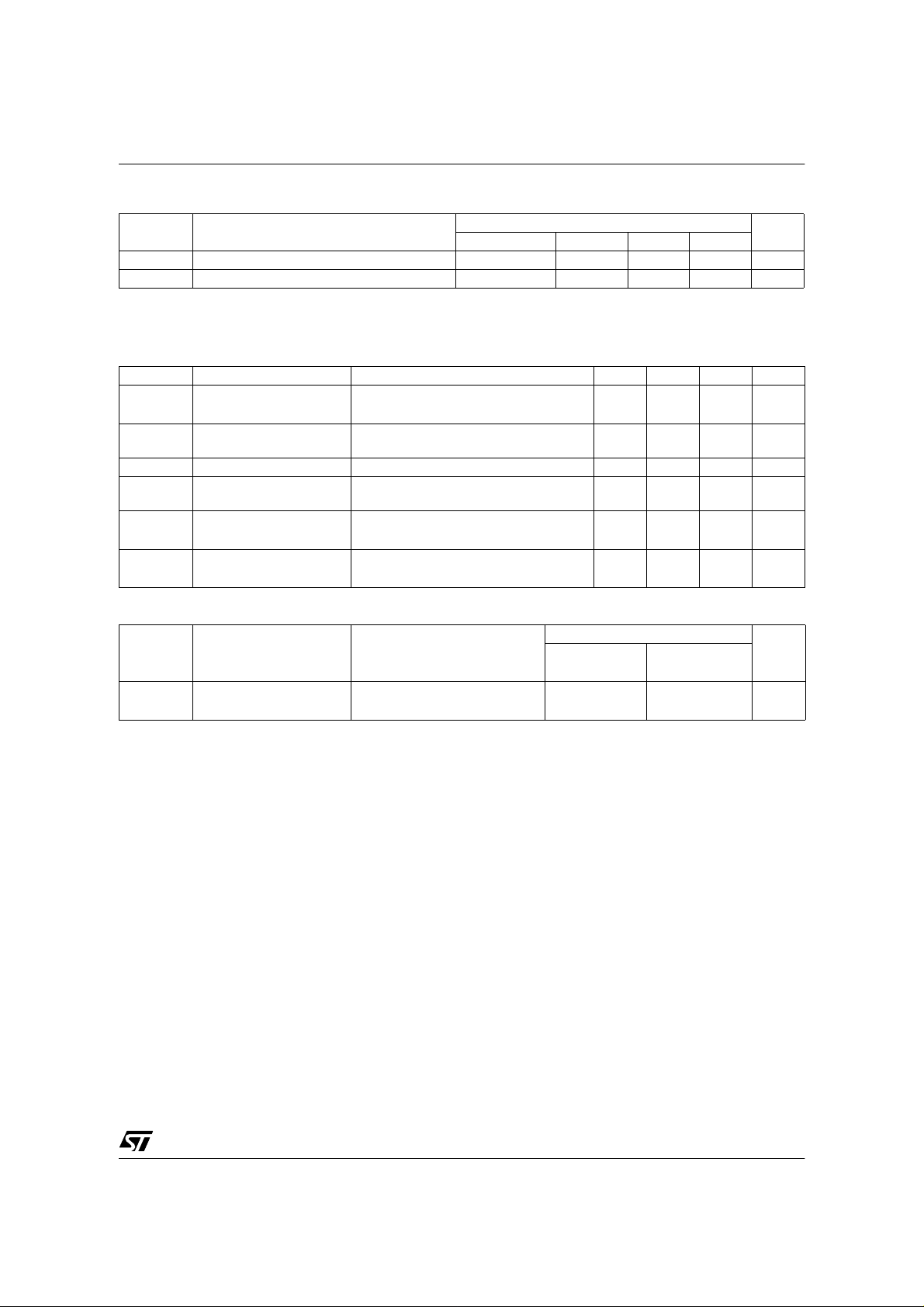
Fig.1: Switching Time Test Circuit for Resistive L oad
V
R
gen
V
gen
I
D
90%
D
t
r
t
V
gen
d(on) t
Fig.2: Test Circuit for Diode Recovery Times
D
I
OMNIFET
S
25 Ω
B
10%
A
R
FAST
DIODE
gen
d(off)
I
OMNIFET
t
f
t
t
A
L=100uH
B
D
V
DD
6/19
V
gen
S
8.5 Ω
Page 7

VNB35NV04 / VNP35NV04 / VNV35NV04 / VNW35NV04
Fig. 3: Unclamped Inductive Load Test Circuits
R
V
IN
P
GEN
W
Fig. 5: Input Ch arge Test Circuit
IN
V
GEN
Fig. 4: Unclamped Inductive Waveforms
Fig 6 : Thermal Impedance for TO-220
Fig. 7:Thermal Impedance for TO-247
ND8003
7/19
Page 8

VNB35NV04 / VNP35NV04 / VNV35NV04 / VNW35NV04
Source-Drain Diode Forward Characteristics Static Drain Source On Resistance
Vsd (mV)
950
Rds(on) (mOhm)
50
900
Vin=0V
850
800
750
700
650
0 5 10 15 20 25 30 35
Id (A)
PowerSO-10 Static Drain-Source On resistance Vs.
Input Voltage
Rds(on) (mOhm)
27.5
25
Id=15A
22.5
17.5
12.5
Id=7.5A
20
Id=15A
Id=7.5A
15
Id=15A
Id=7.5A
10
7.5
5
22.533.544.555.566.5
Tj=150°C
Tj=25°C
Tj=-40°C
Vin (V)
PowerSO-10 Static Drain-Source On Resistance
Vs. Id
Rds(on) (mOhm)
30
25
Vin=5V
20
15
10
5
0
0 5 10 15 20 25 30 35
Id (A)
Tj=150ºC
Tj=25ºC
Tj=-40ºC
Vin=2.5V
40
30
20
10
0123456
Tj=-40ºC
Tj=25ºC
Tj=150ºC
Id (A)
D2PAK, TO-220 & TO-247 Static Drain-Source On
resistance Vs. Input Voltage
Rds(on) (mOhm)
30
25
Tj=150ºC
20
15
10
5
0
2.5 3 3.5 4 4.5 5 5.5 6 6.5
Tj=25ºC
Tj=-40ºC
Id=15A
Id=7.5A
Id=15A
Id=7.5A
Id=15A
Id=7.5A
Vin (V)
D2PAK, TO-220 & TO-247 Static Drain-Source On
Resistance Vs. Id
Rds(on) (mOhm)
24
21
18
15
12
9
6
3
0
0 4 8 121620242832
Vin=5V
Id (A)
Tj=150ºC
Tj=25ºC
Tj=-40ºC
8/19
Page 9

VNB35NV04 / VNP35NV04 / VNV35NV04 / VNW35NV04
Transconductance Transfer Characteristics
Gfs (S)
54
48
42
36
30
24
18
12
6
0
Vds=13V
0 4 8 121620242832
Output Characteristics
Id (A)
55
50
45
40
35
30
25
20
15
10
5
0
0 0.25 0.5 0.75 1 1.25 1.5 1.75 2 2.25 2.5
Vin=4.5V
Vin=4V
Vin=3.5V
Turn On Current Slope
Id (A)
Vds (V)
Vin=3V
Tj=-40ºC
Tj=25ºC
Tj=150ºC
Vin=2.5V
Idon (A)
50
45
40
35
30
25
20
15
10
Vds=13.5V
Tj=-40ºC
Tj=150ºC
Tj=25ºC
5
0
1 1.5 2 2.5 3 3.5 4 4.5 5 5.5 6 6.5
Vin (V)
Normalized On Resistance Vs. Temperature
Rds(on) (mOhm)
4
3.5
3
2.5
2
1.5
1
0.5
0
Vin=5V
Id=15A
-50 -25 0 25 50 75 100 125 150 175
Tc (ºC)
Turn On Current Slope
di/dt (A/us)
20
17.5
15
12.5
10
7.5
5
2.5
0
0 150 300 450 600 750 900 1050
Vin=5V
Vdd=15V
Id=15A
Rg (Ohm)
di/dt (A/us)
10
9
8
7
6
5
4
3
2
0
Vin=3.5V
Vdd=15V
Id=15A
1
0 125 250 375 500 625 750 875 1000 1125
Rg (Ohm)
9/19
Page 10

VNB35NV04 / VNP35NV04 / VNV35NV04 / VNW35NV04
Input Voltage Vs. Input Charge
Vin (V)
8
7
6
5
4
3
2
1
0
0 25 50 75 100 125 150 175
Vds=12V
Id=15A
Qg (nC)
Turn Off Drain-Source Voltage Slope
dV/dt (V/us)
160
140
120
100
80
60
40
20
0
0 150 300 450 600 750 900 1050
Vin=3.5V
Vdd=15V
Id=15A
Rg (Ohm)
Switching Time Resistive Load
T (ns)
1750
tr
1500
1250
1000
750
tf
500
250
0
3 3.5 4 4.5 5 5.5 6 6.5 7
Vdd=15V
Id=15A
Rg=4.7ohm
Vin (V)
td(off)
td(on)
Turn off drain source voltage slope
dV/dt (V/us)
160
140
120
100
80
60
40
20
0
0 150 300 450 600 750 900 1050
Vin=5V
Vdd=15V
Id=15A
Rg (Ohm)
Switching Time Resistive Load
T (us)
40
35
30
25
20
15
10
5
0
Vdd=15V
Id=15A
Rg=4.7ohm
0 300 600 900 1200 1500 1800 2100 2400
Rg (Ohm)
Normalized Input Threshold Voltage Vs.
Temperature
Vinth (V)
2
1.75
1.5
1.25
0.75
0.5
0.25
Vds=Vin
Id=1mA
1
0
-50 -25 0 25 50 75 100 125 150 175
Tc (ºC)
td(off)
tf
tr
td(on)
10/19
Page 11

VNB35NV04 / VNP35NV04 / VNV35NV04 / VNW35NV04
Current Limit Vs. Junction Temperature
Ilim (A)
100
90
80
70
60
50
40
30
20
10
0
Vin=6V
Vds=13V
-50 -25 0 25 50 75 100 125 150 175
Tc (ºC)
Derating Curve
Step Response Current Limit
Tdlim (us)
180
160
Vin=6V
140
120
100
80
60
40
0 5 10 15 20 25 30 35
Vdd (V)
11/19
Page 12

VNB35NV04 / VNP35NV04 / VNV35NV04 / VNW35NV04
TO-220 MECHANICAL DATA
DIM.
mm. inch
MIN. TYP MAX. MIN. TYP. MAX.
A 4.40 4.60 0.173 0.181
C 1.23 1.32 0.048 0.051
D 2.40 2.72 0.094 0.107
E 0.49 0.70 0.019 0.027
F 0.61 0.88 0.024 0.034
F1 1.14 1.70 0.044 0.067
F2 1.14 1.70 0.044 0.067
G 4.95 5.15 0.194 0.203
G1 2.4 2.7 0.094 0.106
H2 10.0 10.40 0.393 0.409
L2 16.4 0.645
L4 13.0 14.0 0.511 0.551
L5 2.65 2.95 0.104 0.116
L6 15.25 15.75 0.600 0.620
L7 6.2 6.6 0.244 0.260
L9 3.5 3.93 0.137 0.154
M 2.6 0.102
DIA. 3.75 3.85 0.147 0.151
.
#
%
.
C
K
*
&
.
8
.
& /
.
.
.
(
(
'
8
)
*
)
(
12/19
Page 13

VNB35NV04 / VNP35NV04 / VNV35NV04 / VNW35NV04
TO-247 MECHANICAL DATA
DIM.
A 4.7 5.3 0.185 0.209
D 2.2 2.6 0.087 0.102
E 0.4 0.8 0.016 0.031
F 1 1.4 0.039 0.055
F3 2 2.4 0.079 0.094
F4 3 3.4 0.118 0.134
G 10.9 0.429
H 15.3 15.9 0.602 0.626
L 19.7 20.3 0.776 0.779
L3 14.2 14.8 0.559 0.582
L4
L5
M 2 3 0.079 0.118
Dia. 3.55 3.65 0.140 0.144
MIN. TYP MAX. MIN. TYP. MAX.
mm. inch
34.6 1.362
5.5
0.217
13/19
11
Page 14

VNB35NV04 / VNP35NV04 / VNV35NV04 / VNW35NV04
PowerSO-10™ MECHANICAL DATA
DIM.
MIN. TYP MAX. MIN. TYP. MAX.
mm. inch
A 3.35 3.65 0.132 0.144
A (*) 3.4 3.6 0.134 0.142
A1 0.00 0.10 0.000 0.004
B 0.40 0.60 0.016 0.024
B (*) 0.37 0.53 0.014 0.021
C 0.35 0.55 0.013 0.022
C (*) 0.23 0.32 0.009 0.0126
D 9.40 9.60 0.370 0.378
D1 7.40 7.60 0.291 0.300
E 9.30 9.50 0.366 0.374
E2 7.20 7.60 0.283 300
E2 (*) 7.30 7.50 0.287 0.295
E4 5.90 6.10 0.232 0.240
E4 (*) 5.90 6.30 0.232 0.248
e 1.27 0.050
F 1.25 1.35 0.049 0.053
F (*) 1.20 1.40 0.047 0.055
H 13.80 14.40 0.543 0.567
H (*) 13.85 14.35 0.545 0.565
h 0.50 0.002
L 1.20 1.80 0.047 0.070
L (*) 0.80 1 .10 0.031 0.043
α 0º 8º 0º 8º
α (*) 2º 8º 2º 8º
(*) Muar only POA P013P
14/19
HE
h
A
F
A1
10
1
eB
0.25
D
= =
D1
= =
E2
DETAIL "A"
DETAIL "A"
B
0.10 A
SEATING
PLANE
A
C
α
E
B
E4
SEATING
PLANE
A1
L
P095A
11
1
1
1
Page 15

VNB35NV04 / VNP35NV04 / VNV35NV04 / VNW35NV04
2
D
PAK MECHANICAL DATA
DIM.
A4.4 4.6
A1 2.49 2.69
A2 0.03 0.23
B 0.7 0.93
B2 1.14 1.7
C 0.45 0.6
C2 1.23 1.36
D 8.95 9.35
D1 8
E10 10.4
E1 8.5
G 4.88 5.28
L 15 15.85
L2 1.27 1.4
L3 1.4 1.75
M2.4 3.2
R0.4
V2 0º8º
MIN. TYP MAX.
mm.
P011P6
15/19
Page 16

VNB35NV04 / VNP35NV04 / VNV35NV04 / VNW35NV04
TO-220 TUBE SHIPMENT (no suffix)
A
Base Q.ty 50
Bulk Q.ty 1000
Tube length (± 0.5) 532
B
A 5.5
B 31.4
C (± 0.1) 0.75
All dimensions are in mm.
C
16/19
Page 17

VNB35NV04 / VNP35NV04 / VNV35NV04 / VNW35NV04
PowerSO-10™ SUGGESTED PAD LAYOUT
14.6 - 14.9
10.8 - 11
6.30
0.67 - 0.73
1
2
3
9.5
4
5
10
0.54 - 0.6
9
8
7
1.27
6
TAPE AND REEL SHIPMENT (suffix “13TR”)
TUBE SHIPMENT (no suffix)
C
A
B
A
All dimensi ons ar e in mm.
Base Q.ty Bulk Q.ty Tube length (± 0.5) A B C (± 0.1)
Casablanca 50 1000 532 10.4 16.4 0.8
Muar 5 0 1000 532 4.9 17.2 0.8
MUARCASABLANCA
B
REEL DIMENSIONS
Base Q.ty 600
Bulk Q.ty 600
A (max) 330
B (min) 1.5
C (± 0.2) 13
F 20.2
G (+ 2 / -0) 24.4
N (min) 60
T (max) 30. 4
C
TAPE DIMENSIONS
According to Electronic Industries Association
(EIA) Standard 481 rev. A, Feb 1986
Tape width W 24
Tape Hole Spacing P0 (± 0.1) 4
Component Spacing P 24
Hole Diameter D (± 0.1/-0) 1.5
Hole Diameter D1 (min) 1.5
Hole Position F (± 0.05) 11.5
Compartm ent Depth K (max) 6.5
Hole Spacing P 1 (± 0.1) 2
All dimensions are in mm.
Top
cover
tape
End
500mm min
All dimensions are in mm.
Empty components pockets
saled with cover tape.
User direction of feed
500mm min
Start
No componentsNo components Components
17/19
1
Page 18

VNB35NV04 / VNP35NV04 / VNV35NV04 / VNW35NV04
D2PAK FOOTPRINT TUBE SHIPMENT (no suffix)
12.20
9.75
16.90
A
C
5.08
1.60
3.50
All dimensions
are in millimeters
B
TAPE AND REEL SHIPMENT (suffix “13TR”)
Base Q.ty 50
Bulk Q.ty 500
Tube length (± 0.5) 532
A 6
B 21.3
C (± 0.1) 0.6
All dimensions are in mm.
REEL DIMENSIONS
Base Q.ty 1000
Bulk Q.ty 1000
A (max) 330
B (min) 1.5
C (± 0.2) 13
F 20.2
G (+ 2 / -0) 24.4
N (min) 60
T (max) 30. 4
All dimensions are in mm.
TAPE DIMENSIONS
According to Electronic Industries Association
(EIA) Standard 481 rev. A, Feb 1986
Tape width W 24
Tape Hole Spacing P0 (± 0.1) 4
Component Spacing P 16
Hole Diameter D (± 0.1/-0) 1.5
Hole Diameter D1 (min) 1.5
Hole Position F (± 0.05) 11.5
Compartm ent Depth K (max) 6.5
Hole Spacing P 1 (± 0.1) 2
All dimensions are in mm.
18/19
Top
cover
tape
End
500mm min
Empty components pockets
saled with cover tape.
User direction of feed
Start
No componentsNo components Components
500mm min
Page 19

VNB35NV04 / VNP35NV04 / VNV35NV04 / VNW35NV04
Information furnished is believed to be ac c ur ate and reliable. However, STMicroel ec tronics assumes no responsi bility for the co nsequences
of use of such information nor for any infringement of patents or other rights of third parties which may results from its use. No license is
granted by implication or oth er wise under any pa tent or patent righ ts of STMicroelec tronics. Specifications ment ioned in this publication are
subject to c hange without notice. This p ublication supersedes and replaces all information p r ev iously supplied. STMicroelectronics pr oducts
are not authorized for use as critical components in life support devices or systems without express written approval of STMicroelectronics.
Australia - Brazil - China - Finland - France - Germany - Hong Kong - India - Italy - Japan - Malaysia - Malta - Morocco -
Singapore - Spain - Sweden - S witzerland - Unit ed K ingdom - U.S.A.
The ST logo is a trademark of STM ic r oelectronics
2003 STMicroelectronics - P r inted in IT A LY- All Rig hts Reserved.
STMicroelectronics GROUP OF COMPANIES
http://www.st.com
19/19
 Loading...