

Page 1
®
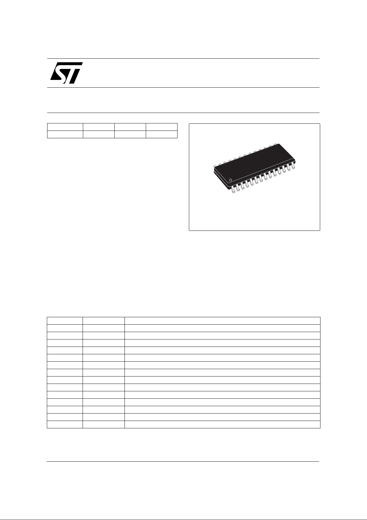
VN772K
QUAD SM ART P OWE R SOL ID STATE RE LAY
FOR COMP LET E H B RIDG E CO NF IGUR ATIONS
TYPE R
VN772K 120 mΩ (*) 9A (**) 36V
(*) Total resis tance of one side in bridge configuration
(**) Typica l c ur r ent limitation value
■ SUITED AS LOW VOLTAGE BRIDGE
■ LINEAR CURRENT LIMITATION
■ VERY LOW STAND-BY POWER DISSIPATION
■ SHORT CIRCUIT PROTECTED
■ DOUBLE STATUS FLAG DIAGNOSTIC (OPEN
DS(on)
I
OUT
V
CC
DRAIN)
■ INTEGRATED CLAMPING CIRCUITS
■ UNDERVOLTAGE PROTE CTIO N
■ ESD PROTECTION
DESCRIPTION
The VN772K is a device formed by three
monolithic chips housed in a standard SO-28
package: a double high side and two low side
switches. Both the d ouble high si de an d low side
switches are made using |STMicroelectronics
VIPower™ M0-3 Technology. This device is
suitable to drive a DC motor in a bridge
configuration as well as to be used as a quad
switch for any low voltage application. The dual
SO-28
high side switches have bui lt-i n ther mal s hutdo wn
to protect the chips from overtemperature and
current limiter blocks to protect the device from
short circuit. Statu s output is provi ded to indicate
open load in off and on state and overtemperature.
The low sid e swi tches are two O MNIFET II typ es
(fully autopr otecte d Powe r MOSF ET in V IPower™
technology). They have built-in thermal shutdown,
linear current limitation and overvoltage clamping.
Fault feedback for thermal intervention can be
detected by monitoring the voltage at the input pin.
PIN FUNCTION
No NAME FUNCTION
1, 3, 25, 28 DRAIN 3 Drain of Switch 3 (low-side switch)
2 INPUT 3 Input of Switch 3 (low-side switch)
4, 11 N.C. Not Connected
5, 10, 19, 24 V
6 GND Ground of Switches 1 and 2 (high-side switche s)
7 INPUT 1 Input of Switch 1 (high-side swi tches)
8 DIAGNOSTIC Diagn ostic of Sw itches 1 and 2 (high-side swit ches)
9 INPUT 2 Input of Switch 2 (high-side swi tch)
12, 14, 15, 18 DRAIN 4 Drain of switch 4 (low-side switch)
13 INPUT 4 Input of Switch 4 (low-side switch)
16, 17 SOURCE 4 Source of Switch 4 (l ow-side switch)
20, 21 SOURCE 2 Source of Switch 2 (hi gh-side switch)
22, 23 SOURCE 1 Source of Switch 1 (hi gh-side switch)
26, 27 SOURCE 3 Source of Switch 3 (l ow-side switch)
November 2002 1/21
CC
Drain of Switches 1 and 2 (high-side switches) and Power Supply Voltage
1
Page 2
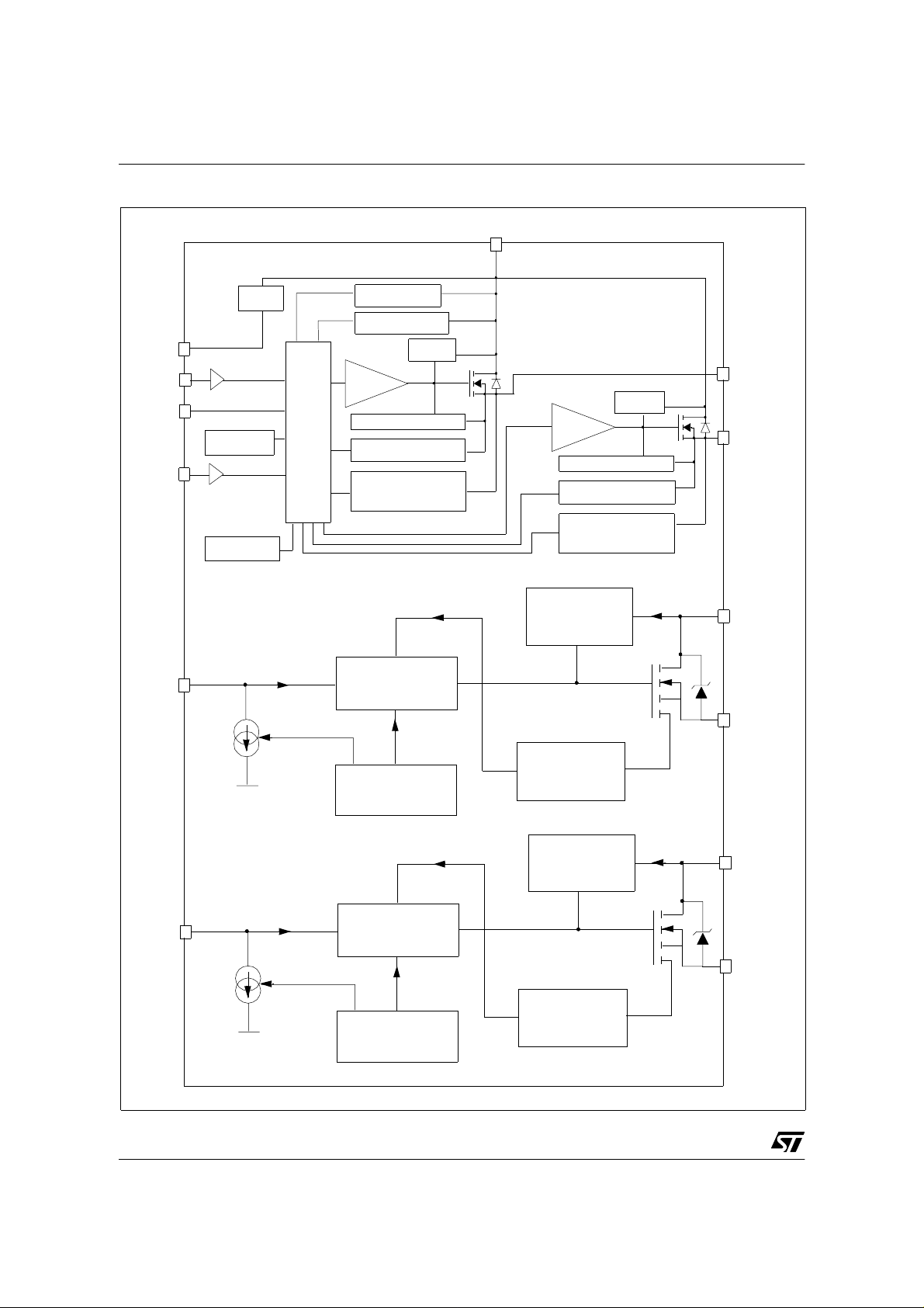
VN772K
BLO C K DIAG RA M
V
cc
CLAMP
OVERVOLTAGE
UNDERVOLTAGE
V
cc
GND
INPUT1
DIAG
INPUT2
INPUT3
OVERTEMP. 1
OVERTEMP. 2
LOGIC
CLAMP 1
DRIVER 1
CURRENT LIMITER 1
OPENLOAD ON 1
OPENLOAD OFF 1
Gate
Control
Over
T emperature
DRIVER 2
CURRENT LIMITER 2
OPENLOAD ON 2
OPENLOAD O FF 2
Overvoltage
Clamp
Linear
Current
Limiter
SOURCE1
CLAMP 2
SOURCE2
DRAIN3
SOURCE3
2/21
1
INPUT4
Gate
Control
Over
T emperature
Overvoltage
Clamp
Linear
Current
Limiter
DRAIN4
SOURCE4
Page 3
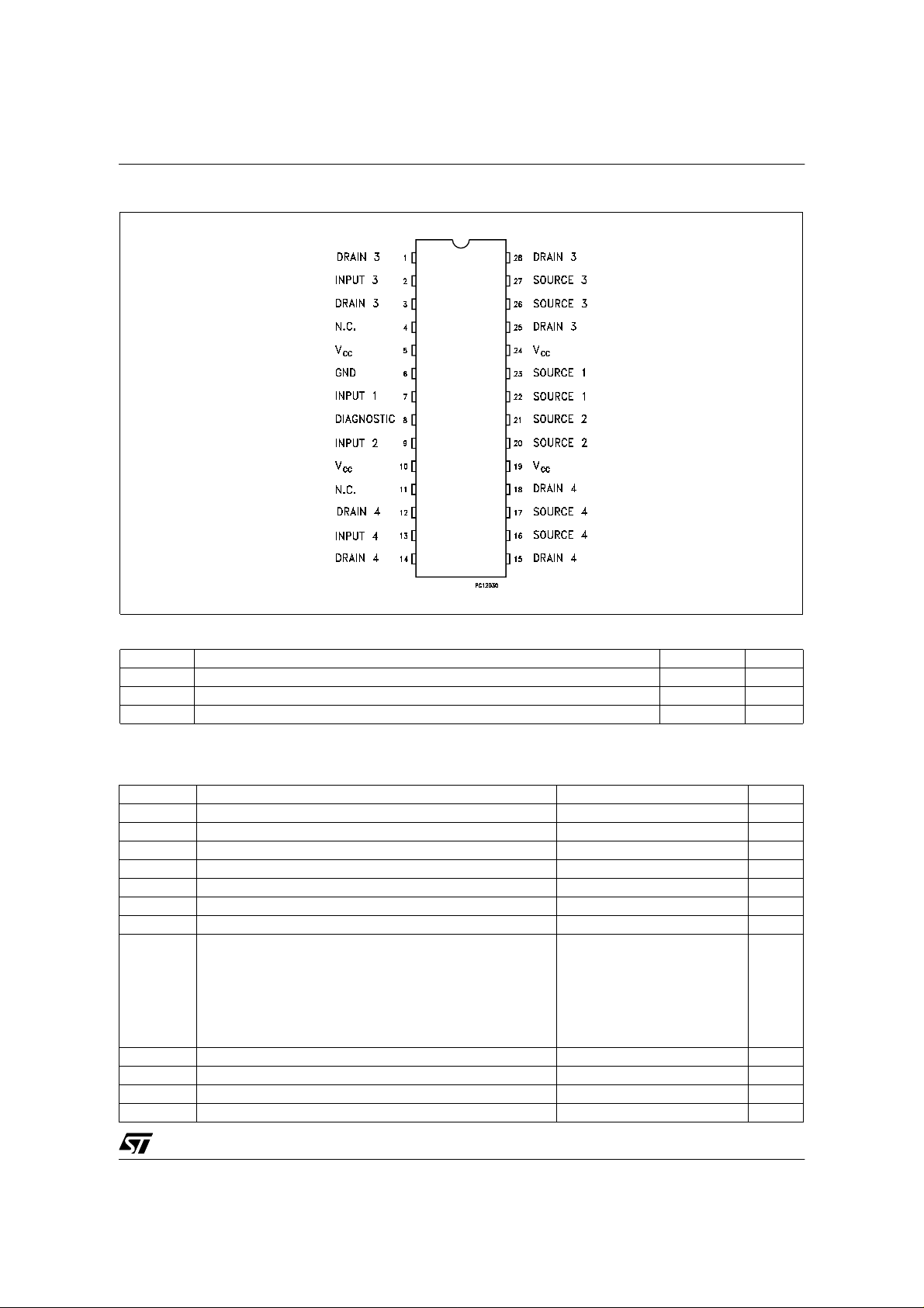
CONNECTION DIAGRAM
VN772K
THERMAL DATA
Symbol Parameter Value Unit
R
thj-case
R
thj-case
R
thj-amb
Thermal Resist ance Junction-case (High-side switch) MAX 20 °C/W
Thermal Resist ance Junction-case (Low-side switch) MAX 20 °C/W
Thermal Resist ance Junction-ambient MAX 60 °C/W
ABSOLUTE MAXIMUM RATI NG
DUAL HIGH SIDE SWITCH
Symbol Parameter Value Unit
tot
DC Supply Voltage 41 V
Reverse DC Supply Voltage - 0.3 V
CC
DC Reverse Ground Pin Current - 200 mA
DC Output Current Internally Limited A
Reverse DC Output Current - 6 A
DC Input Current +/- 10 mA
DC Status Cur rent +/- 10 mA
Electrostatic Discharge (Human Body Model: R=1.5KΩ;
C=100pF)
- INPUT
- STATUS
- OUTPU T
- V
CC
4000
4000
5000
5000
Powe r Dissipation Tc=25°C 6 W
Junction Operating Temperature Internally Limited °C
j
Case Operating Temperature - 40 to 150 °C
c
Storage Temperature - 55 to 150 °C
V
- V
- I
I
OUT
- I
I
STAT
V
P
T
CC
GND
OUT
I
IN
ESD
T
T
stg
V
V
V
V
3/21
1
Page 4
VN772K
ABSOLUTE MAXIMUM RATING (continued)
LOW SIDE SWITCHES
Symbol Parameter Value Unit
V
DS
V
IN
I
IN
R
IN MIN
I
D
I
R
V
ESD1
V
ESD2
P
tot
T
j
ELECTRICAL CHARACTERISTICS FOR DUAL HIGH SIDE SWITCH
(8V<VCC<36V; -40°C< Tj <150°C, unless otherwise specified)
POWER OUTPUTS (Per each channel)
Symbol Parameter Test Conditions Min Typ Max Unit
(**) Operating Supply Voltag e 5.5 13 36 V
V
CC
(**) Undervol tage Shut -down 3 4 5.5 V
V
USD
(**) Overv olt age Shut-d ow n 36 V
V
OV
R
DS(on)
(**) Supply Current
I
S
I
L(off1)
I
L(off2)
I
L(off3)
I
L(off4)
Drain-source Voltage (VIN=0V) Internally Clampe d V
Input Voltage Internally Clamped V
Input Current +/-20 mA
Minim um Input Series Impe dance 150 Ω
Drain Current Inte rnally Lim ited A
Reverse DC Output Current -10.5 A
Electrostat ic Dischar ge (R=1.5KΩ , C=100pF) 4000 V
Electrostat ic Dischar ge on output pin only
(R=330Ω, C=150pF)
16500 V
Power Dissipation (TC=25°C) 6 W
Opera ting Junct ion Temperature Internally limited °C
I
=2A; Tj=25°C
On State Resistance
OUT
I
=2A; VCC>8V
OUT
Off Stat e; V
Off Stat e; V
V
IN=VOUT
On State; V
Off State Output Current VIN=V
OUT
Off State Output Current VIN=0V; V
Off State Output Current VIN=V
Off State Output Current VIN=V
OUT
OUT
=13V; V
CC
=13V; Tj =25°C;
CC
=0V
=13V
CC
IN=VOUT
=0V
12
12
5
=0V; VCC=36V; Tj=125°C 0 50 µA
=3.5V -75 0 µA
OUT
=0V; VCC=13V; Tj =125°C 5 µA
=0V; VCC=13V; Tj =25°C 3 µA
60
120
40
25
7
mΩ
mΩ
µA
µA
mA
SWITCHING (Per each channel) (VCC=13V)
Symbol Parameter Test Condit ions Min Typ Max U nit
t
d(on)
t
d(off)
dV
OUT
dt
(on)
dV
OUT
dt
(off)
(**) Per device
4/21
Turn-on Delay Time
Turn-off Delay Time
/
Turn-on Voltage Slope
/
Turn-off Voltage Slope
RL=6.5Ω from VIN rising edge to
V
=1.3V
OUT
RL=6.5Ω from VIN falling edge to
V
=11.7V
OUT
RL=6.5Ω from V
=10.4V
V
OUT
RL=6.5Ω from V
V
=1.3V
OUT
=1.3V to
OUT
=11.7V to
OUT
30 µs
30 µs
See
relative
diagram
See
relative
diagram
V/µs
V/µs
Page 5
VN772K
ELECTRICAL CHARACTERISTICS FOR DUAL HI GH SIDE SWITCH (continued)
INPUT PINS (Per each channel)
Symbol Parameter Test Conditions Min Typ Max Unit
V
I
V
I
IH
V
I(hyst)
V
ICL
LOGIC INPUT (Per each channel)
Symbol Parameter Test Conditions Min Typ Max Unit
V
I
V
I
IH
V
I(hyst)
V
ICL
STATUS PIN (Per each channel)
Symbol Parameter Test Conditions Min Typ M ax Unit
V
STAT
I
LSTAT
C
STAT
V
SCL
Input Low Level 1.25 V
IL
Low Level Input Current VIN=1.25V 1 µA
IL
Input High Level 3.25 V
IH
High Level Input Current VIN=3.25V 10 µA
Input Hyst eresis Vo lt age 0.5 V
=1mA
I
Input Clamp Voltage
Input Low Level 1.25 V
IL
Low Level Input Current VIN = 1.25V 1 µA
IL
Input High Level 3.25 V
IH
IN
I
= -1mA
IN
6.5 7.4
-0.7
High Level Input Current VIN = 3.25V 10 µA
Input Hyst eresis Vo lt age 0.5 V
= 1mA
I
Input Clamp Voltage
Status Low Output Voltage I
IN
I
= -1mA
IN
= 1.6 mA 0.5 V
STAT
Status Leakage Current Normal Operation; V
Status Pin Input
Capacitance
Status Clamp Voltage
Normal Operation; V
= 1mA
I
STAT
I
= - 1mA
STAT
= 5V 10 µA
STAT
= 5V 100 pF
STAT
66.8
-0.7
66.8
-0.7
8.5 V
8V
8V
V
V
V
PROTECTIONS (Per each channel)
Symbol Parameter Test Condit ions M in Typ Max Unit
T
T
t
SDL
I
V
demag
TSD
T
hyst
lim
Shut-down Temperature 150 175 200 °C
Reset Temp erature 135 °C
R
Ther ma l Hy steresi s 7 15 °C
Status Delay in Overload
Conditions
Current limitation T
Tj>T
=125°C
j
TSD
8.5
6
915
5.5V<VCC<36V
Turn-off Output Clamp
Voltage
=2A; L= 6m H VCC-41 VCC-48 VCC-55 V
I
OUT
20 µs
15
15
A
A
A
5/21
1
Page 6
VN772K
ELECTRICAL CHARACTERISTICS FOR DUAL HI GH SIDE SWITCH (continued)
OPENLOAD DETECTION (Per each channel)
Symbol Parameter Test Conditions Min Typ Max Unit
I
OL
t
DOL(on)
V
T
DOL(off)
Openload ON State
Detectio n Threshol d
Openload ON State
Detection Delay
=5V 50 100 200 mA
V
IN
=0A 200 µs
I
OUT
Openload OFF State
Voltage Detection
OL
Threshold
Openload Detection Delay
at Turn Off
VIN=0V 1.5 2.5 3.5 V
1000 µs
6/21
Page 7
VN772K
ELECTRICAL CHARACTERISTICS FOR LOW SIDE SWITCHES
(-40°C < Tj < 150°C, unless otherwise specified)
OFF
Symbol Parameter Test Conditions Min Typ Max Unit
V
CLAMP
V
CLTH
V
I
V
I
DSS
INTH
ISS
INCL
Drain-source Clamp
Voltage
Drain-source Clamp
Threshold Voltage
Input Threshold Voltage VDS=VIN; ID=1mA 0.5 2.5 V
Supply Cur rent fro m Inpu t
Pin
Input-Source Clamp
Voltage
Zero Input Voltage Drain
Current (VIN=0V)
ON
Symbol Parameter Test Conditions Min Typ Max Unit
R
DS(on)
Stati c Dr ain-sourc e On
Resist an ce
(Tj=25°C, unless otherwise specified)
DYNAMIC
Symbol Parameter Test Conditions Min Typ Max Unit
Forward
(*)
g
fs
C
OSS
Transconductance
Output Capacitance VDS=13V; f=1MHz; VIN=0V 220 pF
VIN=0V; ID=3.5A 40 45 55 V
VIN=0V; ID=2mA 36 V
VDS=0V; VIN=5V 100 150 µA
=1mA
I
IN
I
=-1mA
IN
=13V; VIN=0V; Tj=25°C
V
DS
V
=25V; VIN=0V
DS
=5V; ID=3.5A; Tj=25°C
V
IN
V
=5V; ID=3.5A
IN
6
-1.0
6.8 8
-0.3
30
75
60
120
VDD=13V; ID=3.5A 9 S
V
µA
mΩ
SWITCHING
Symbol Parameter Test Conditions Min Typ M ax Unit
t
d(on)
t
t
d(off)
t
t
d(on)
t
t
d(off)
t
(dI/dt)
Q
Turn-on Delay Time
Rise Time 470 1500 ns
r
Turn-off Delay Time 500 1500 ns
Fall Time 350 1000 ns
f
VDD=15V; ID=3.5A
V
=5V; R
gen
gen=RIN MIN
=150Ω
Turn-on Delay Time
Rise Time 4.6 14.0 µs
r
Turn-off Dela y Tim e 5.4 16.0 µs
Fall Ti me 3.6 11.0 µs
f
Turn-on Current Slope
on
Total In put Charge
i
VDD=15V; ID=3.5A
V
=5V; R
gen
=15V; ID=3.5A
V
DD
V
=5V; R
gen
=12V; ID=3.5A; VIN=5V
V
DD
I
=2.13mA
gen
=2.2KΩ
gen
gen=RIN MIN
=150Ω
100 300 ns
0.75 2.3 µs
6.5 A/µs
18 nC
SOURCE DRAIN DIODE
Symbol Parameter Tes t Conditions Min Typ Max Unit
(*) Forward On Voltage ISD=3.5A; VIN=0V 0.8 V
V
SD
Q
I
RRM
t
Reverse Recovery Time
rr
Reverse Recovery Charge 0.28 µC
rr
Reverse Re covery C urrent 2.5 A
=3.5A; dI/dt=20A/µs
I
SD
V
=30V; L= 20 0 µ H
DD
220 ns
7/21
Page 8

VN772K
ELECTRICAL CHARACTERISTICS FOR LOW SIDE SWITCHES (continued)
PROTECTIONS (-40°C < Tj < 150°C, unless otherwise specified)
Symbol Parameter Test Conditions Min Typ Max Unit
V
=5V; VDS=13V
I
lim
t
dlim
T
jsh
T
I
E
(*) Pulsed: Pulse dura tion = 300µs, duty cycle 1.5%
Drain C urr en t Lim it
Step Response Current
Limit
Overtem perature
Shutdown
Overt em peratur e Reset 135 °C
jrs
Fault Si nk Current VIN= 5V; VDS=13V; Tj=T
gf
Single Pu lse
as
Avalanche Energy
IN
V
=5V; VDS=13V; T
IN
V
=5V; VDS=13V
IN
starting T
V
IN
=25°C; VDD=24V
j
=5V; R
gen=RIN MIN
=125°C
j
jsh
=150Ω; L=24mH
6
91212A
6.5
4.0 µs
150 175 °C
15 mA
200 mJ
A
8/21
Page 9

SWITCHING TIME WAVEFORMS
V
OUTn
80%
/dt
dV
OUT
(on)
V
INn
t
d(on)
DUAL HIGH-SIDE SWI TCH
10%
t
d(off)
90%
dV
OUT
/dt
VN772K
(off)
t
t
TRUTH TABLE
CONDITIONS INPUT OUTPUT STATUS
Normal Operation
Current Limitation
Overtemperature
Undervoltage
Overvoltage
Output Voltage > V
Output Current < I
OL
OL
OPEN LOAD STATUS TIMING (with external pu ll -up)
V
> V
OUT
V
INn
V
STAT n
L
H
L
H
H
L
H
L
H
L
H
L
H
L
H
OL
I
OUT
< I
OL
V
INn
V
STAT n
L
H
L
X
X
(T
(T
< T
j
> T
j
L
L
L
L
L
L
H
H
L
H
OVER TEMP STATUS TIMING
Tj > T
t
SDL
TSD
TSD
TSD
) H
) L
H
H
H
H
L
X
X
H
H
L
H
H
L
t
SDL
t
DOL(off)
t
DOL(on)
9/21
1
Page 10

VN772K
TYPICAL APPLICATION DIAGRAM
10/21
1
Page 11

Figure1: Waveforms
INPUT
n
OUTPUT VOLTAGE
STATUS
V
CC
INPUT
n
OUTPUT VOLTAGE
STATUS
V
CC
INPUT
n
OUTPUT VOLTAGE
STATUS
VN772K
NORMAL OPERATION
n
n
UNDERVOLTAGE
V
USDhyst
V
USD
n
n
OVERVOLTAGE
VCC<V
OV
n
n
undefined
VCC>V
OV
INPUT
n
OUTPUT VOLTAGE
STATUS
INPUT
n
n
OUTP U T VO LTAG E
STATUS
T
INPUT
n
j
n
OUTPUT CURRENT
STATUS
n
OPEN LOAD wi th external pull-up
n
OPEN LOAD without external pull-up
V
n
T
TSD
T
R
n
V
OL
OVERTEMPE RATURE
OUT>VOL
11/21
11
Page 12

VN772K
ELECTRICAL CHARACTERIZATION FOR DUAL HIGH SIDE SWITCH
Off State Output Current
High Level Input Current
IL(off1) (u A)
2.5
2.25
2
1.75
1.5
1.25
1
0.75
0.5
0.25
0
-50 -25 0 25 50 75 100 125 150 175
Off state
Vcc=36V
Vin=Vout=0V
Iih (uA)
5
4.5
3.5
2.5
1.5
0.5
Vin=3.25V
4
3
2
1
0
-50 -25 0 25 50 75 100 125 150 175
Tc (°C)
Input Clamp Voltage Status Leakage Current
Vicl (V)
8
7.8
7.6
7.4
7.2
7
6.8
6.6
6.4
6.2
6
Iin=1mA
-50 -25 0 25 50 75 100 125 150 175
Tc (°C)
Ilstat (uA)
0.05
0.04
Vstat=5V
0.03
0.02
0.01
0
-50 -25 0 25 50 75 100 125 150 175
Tc (°C)
Tc (°C)
12/21
Vstat (V)
0.8
0.7
Istat=1.6mA
0.6
0.5
0.4
0.3
0.2
0.1
0
-50 -25 0 25 50 75 100 125 150 175
Tc (°C)
Status Clamp VoltageStatus Low Output Voltage
Vscl (V)
8
7.8
7.6
7.4
7.2
6.8
6.6
6.4
6.2
Istat=1mA
7
6
-50 -25 0 25 50 75 100 125 150 175
Tc (°C)
Page 13

ELECTRICAL CHARACTERIZATION FOR DUAL HIGH SIDE SWITCH (continued)
On State Resistance Vs T
case
On State Resistance Vs V
CC
VN772K
Ron (mOhm)
160
140
120
100
80
60
40
20
0
-50 -25 0 25 50 75 100 125 150 175
Iout=2A
Vcc=8V; 13V & 36V
Tc (°C)
Iol (mA)
150
140
130
120
110
100
90
80
70
60
50
Vcc=13V
Vin=5V
-50 -25 0 25 50 75 100 125 150 175
Tc (ºC)
Input High LevelOpenload On State Detection Threshold
Ron (mOhm)
120
110
100
90
80
70
60
50
40
30
20
10
0
5 10152025303540
Tc=150°C
Tc=25°C
Tc= - 40°C
Iout=5A
Vcc (V)
Vih (V)
3.6
3.4
3.2
3
2.8
2.6
2.4
2.2
2
-50 -25 0 25 50 75 100 125 150 175
Tc (°C)
Vil (V)
2.6
2.4
2.2
2
1.8
1.6
1.4
1.2
1
-50 -25 0 25 50 75 100 125 150 175
Tc (°C)
Input Hysteresis VoltageInput Low Level
Vhyst (V)
1.5
1.4
1.3
1.2
1.1
1
0.9
0.8
0.7
0.6
0.5
-50 -25 0 25 5 0 7 5 100 125 150 175
Tc (°C)
13/21
Page 14

VN772K
ELECTRICAL CHARACTERIZATION FOR DUAL HIGH SIDE SWITCH (continued)
Overvoltage Shutdown
Openload Off State Voltage Detection Threshold
Vov (V)
50
48
46
44
42
40
38
36
34
32
30
-50 -25 0 25 50 75 100 125 150 175
Vol (V)
5
4.5
4
3.5
3
2.5
2
1.5
1
0.5
0
Vin=0V
-50 -25 0 25 50 75 100 125 150 175
Tc (°C)
Turn-on Voltage Slope Turn-off Voltage Slope
dVout/dt(on) (V/ms)
800
700
600
500
400
300
200
Vcc=13V
Rl=6.5Ohm
dVout/dt(off) (V/ms)
600
550
500
450
400
350
300
Vcc=13V
Rl=6.5Ohm
Tc (°C)
I
LIM
14/21
100
0
-50 -25 0 25 50 75 100 125 150 175
Tc (ºC)
Vs T
case
Ilim (A)
20
18
16
14
12
10
8
6
4
2
0
Vcc=13V
-50 -25 0 25 50 75 100 125 150 175
Tc (°C)
250
200
-50 -25 0 25 50 75 100 125 150 175
Tc (ºC)
Page 15

VN772K
ELECTRICAL CHARACTERIZATION FOR LOW SIDE SWITCH
Source-Drain Diode Forward Characteristics
Vsd (mV)
1000
950
900
850
800
750
700
650
600
550
500
Vin=0V
0 2 4 6 8 101214
Id(A)
Derating Curve
Static Drain Source On Resistance
Rds(on) (mOhm)
500
450
400
350
300
250
200
150
100
50
0
0 0.25 0.5 0.75 1 1.25
Static Drain-Source On resistance Vs. Input
Voltage
Rds(on) (mOhm)
120
110
100
90
80
70
60
50
40
30
20
10
0
33.544.555.566.57
ES
Tj= - 40ºC
Vin=2.5V
Tj=25ºC
Tj=150ºC
Id(A)
Id=3.5A
Tj=150ºC
Tj=25ºC
Tj= - 40ºC
Vin(V)
Static Drain-Source On resistance Vs. Input
Voltage
Rds(on) (mOhm)
140
120
Tj=150ºC
100
80
Tj=25ºC
60
Tj=-40ºC
40
20
0
3 3.5 4 4.5 5 5.5 6 6.5
Vin(V)
Id=6A
Id=1A
Id=6A
Id=1A
Id=6A
Id=1A
Transconductance
Gfs (S)
20
18
16
14
12
10
8
6
4
2
0
Vds=13V
012345678
Id(A)
Tj=-40ºC
Tj=25ºC
Tj=150ºC
15/21
Page 16

VN772K
ELECTRICAL CHARACTERIZATION FOR LOW SIDE SWITCH
Static Drain-Source On Resistance Vs. Id
Rds(on) (mOhm)
140
120
100
80
60
40
20
0
00.511.522.533.544.555.56
Tj=150ºC
Tj=25ºC
Tj=-40ºC
Vin=3.5V
Vin=5V
Vin=3.5V
Vin=5V
Vin=3.5V
Vin=5V
Id(A)
Turn On Current Slope
di/dt(A/us)
8
7
6
5
4
3
2
1
0
100
200
300
400
500
Rg(ohm)
600
Vin=5V
Vdd=15V
Id=3.5A
700
800
900
1000
1100
Transfer Characteristics
Idon(A)
10
9
8
7
6
5
4
3
2
1
0
1 1.5 2 2.5 3 3.5 4 4.5 5 5.5
Turn On Current Slope
di/dt(A/us)
2.25
2
1.75
1.5
1.25
1
0.75
0.5
0.25
100 200 300 400 500 600 700 800 900 1000 1100
ES
(continued)
Vds=13.5V
Vin(V)
Rg(ohm)
Tj=25ºC
Tj=-40ºC
Tj=150ºC
Vin=3.5V
Vdd=15V
Id=3.5A
Input Voltage Vs. Input Charge
Vin(V)
8
7
6
5
4
3
2
1
0
0 5 10 15 20 25
16/21
Vds=12V
Id=3.5A
Qg(nC)
Turn off drain source voltage slope
dv/dt(V/us)
300
250
200
150
100
50
0
100 200 300 400 500 600 700 800 900 1000 1100
Rg(ohm)
Vin=5V
Vdd=15V
Id=3.5A
Page 17

VN772K
ELECTRICAL CHARACTERIZATION FOR LOW SIDE SWITCH
Turn Off Drain-Source Voltage Slope
dv/dt(v/us)
300
250
700
Vin=3.5V
Vdd=15V
Id=3.5A
800
900
200
150
100
50
0
100
200
300
400
500
600
Rg(ohm)
Switching Time Resistive Load
t(us)
5.5
5
4.5
3.5
2.5
1.5
0.5
Vdd=15V
Id=3.5A
Vin=5V
4
3
2
1
0
250
0
500
750
1000
1250
td(off)
td(on)
1500
1750
2000
Rg(ohm)
1000
2250
1100
tr
tf
2500
Capacitance Variations
C(pF)
600
500
400
300
200
100
0 5 10 15 20 25 30 35
Switching Time Re sist ive Load
t(ns)
1600
1400
1200
1000
800
600
400
200
0
3.25 3.5 3.75 4 4.25 4.5 4.75 5 5.25
ES
tr
(continued)
Vds(V)
td(off)
td(on)
Vin(V)
f=1MHz
Vin=0V
Vdd=15V
Id=3.5A
Rg=150ohm
tf
Output Characteristics
ID(A)
12
11
10
9
8
7
6
5
4
3
2
1
0
012345678910111213
VDS(V)
Vin=5V
Vin=4.5V
Vin=4V
Vin=3V
Vin=2.5V
Vin=2V
Normalized On Resistance Vs. Temperature
Rds(on)
2.25
2
1.75
1.5
1.25
1
0.75
0.5
Vin=5V
Id=3.5A
-50 -25 0 25 50 75 100 125 150 175
T(ºC)
17/21
Page 18

VN772K
ELECTRICAL CHARACTERIZATION FOR LOW SIDE SWITCH
Normalized Input Threshold Voltage Vs.
Current Limit Vs. Junction Temperature
Temperature
Vin(th)
1.15
1.1
1.05
1
0.95
0.9
0.85
0.8
0.75
0.7
-50 -25 0 25 50 75 100 125 150 175
T(ºC)
Vds=Vin
Id=1mA
Ilim (A)
15
14
13
12
11
10
9
8
7
6
5
-50 -25 0 25 50 75 100 125 150 175
Step Response Current Limit
Tdlim(us)
7
6.5
6
Vin=5V
Rg=150ohm
ES
(continued)
Vds=13V
Vin=5V
Tj (ºC)
5.5
5
4.5
4
3.5
5 101520253035
Vdd(V)
18/21
Page 19

SO-28 MECHANICAL DATA
VN772K
DIM.
A 2.65 0.104
a1 0.10 0.30 0.004 0.012
b 0.35 0.49 0.013 0.019
b1 0.23 0.32 0.009 0.012
C 0.50 0.020
c1 45 (typ.)
D 17.7 18.1 0.697 0.713
E 10.00 10.65 0.393 0.419
e 1.27 0.050
e3 16.51 0.650
F 7.40 7.60 0.291 0.299
L 0.40 1.27 0.016 0.050
S8 (max.)
MIN. TYP MAX. MIN. TYP. MAX.
mm. inch
19/21
Page 20

VN772K
SO-28 TUBE SHIPMENT (no suffix)
Base Q.ty 28
Bulk Q.ty 700
C
B
Tube length (± 0.5) 532
A 3.5
B 13. 8
C (± 0.1) 0.6
All dimensions are in mm.
A
TAPE AND REEL SHIPMENT (suffix “13TR”)
REEL DIMENSIONS
Base Q.ty 1000
Bulk Q.ty 1000
A (max) 330
B (min) 1.5
C (± 0.2) 13
F 20.2
G (+ 2 / -0) 16.4
N (min) 60
T (max) 22.4
TAPE DIMENSIONS
According to Elec tronic Industrie s Association
(EIA) S tandard 481 rev. A , Feb 19 86
Tape width W 16
Tape Hole Spacing P0 (± 0.1) 4
Component Spacing P 12
Hole Diameter D (± 0.1/-0) 1.5
Hole Diameter D1 (min) 1.5
Hole Position F (± 0.05) 7.5
Compartment Depth K (max) 6.5
Hole Spacing P1 (± 0.1) 2
All dimensions ar e in mm.
20/21
Top
cover
tape
End
500mm min
Empty components pockets
saled with cover tape.
User direction of feed
Start
No componentsNo components Components
500mm min
Page 21

VN772K
Information furnished is believed to be accurate and r eliable. Howev er, STMicroelectr onics assume s no r es ponsibility for the consequences
of use of such information nor for any infringement of patents or other rights of third parties which may results from its use. No license is
granted by implication or otherwise under any patent or patent rights of STMi c r oelectronic s . Specifications mentioned in this publication are
subject to c hange withou t notice. This publicatio n s upersedes and replaces all informati on previously s upplied. ST M icroelectr on ics product s
are not authorized for use as critical components in life support devices or systems without express written approval of STMicroelectronics.
Australia - Brazil - Canada - Ch ina - Finland - Franc e - Germany - Hong Kong - India - Isra el - Italy - Japan - M alaysia -
Malta - Morocco - Singapore - Spain - Sweden - Switzerland - United Kingdom - U.S.A.
The ST logo is a trademark of ST M ic r oelectronic s
2002 STMicroelectronics - Printed in ITALY- All Rights Reserved.
STMicroelectronics GROUP OF COMPANIES
http://www.st.com
21/21
 Loading...