

Page 1
Features
VN751S
High side driver
Typ e R
DS(on)
I
out
V
CC
VN751S 60 mΩ 2.5 A 36 V
■ CMOS compatible input
■ Thermal shutdown
■ Shorted load protection
■ Undervoltage and overvoltage shutdown
■ Protection against loss of ground
■ Very low standby current
■ Compliance to 61000-4-4 IEC test up to 4 kV
■ Open drain status output
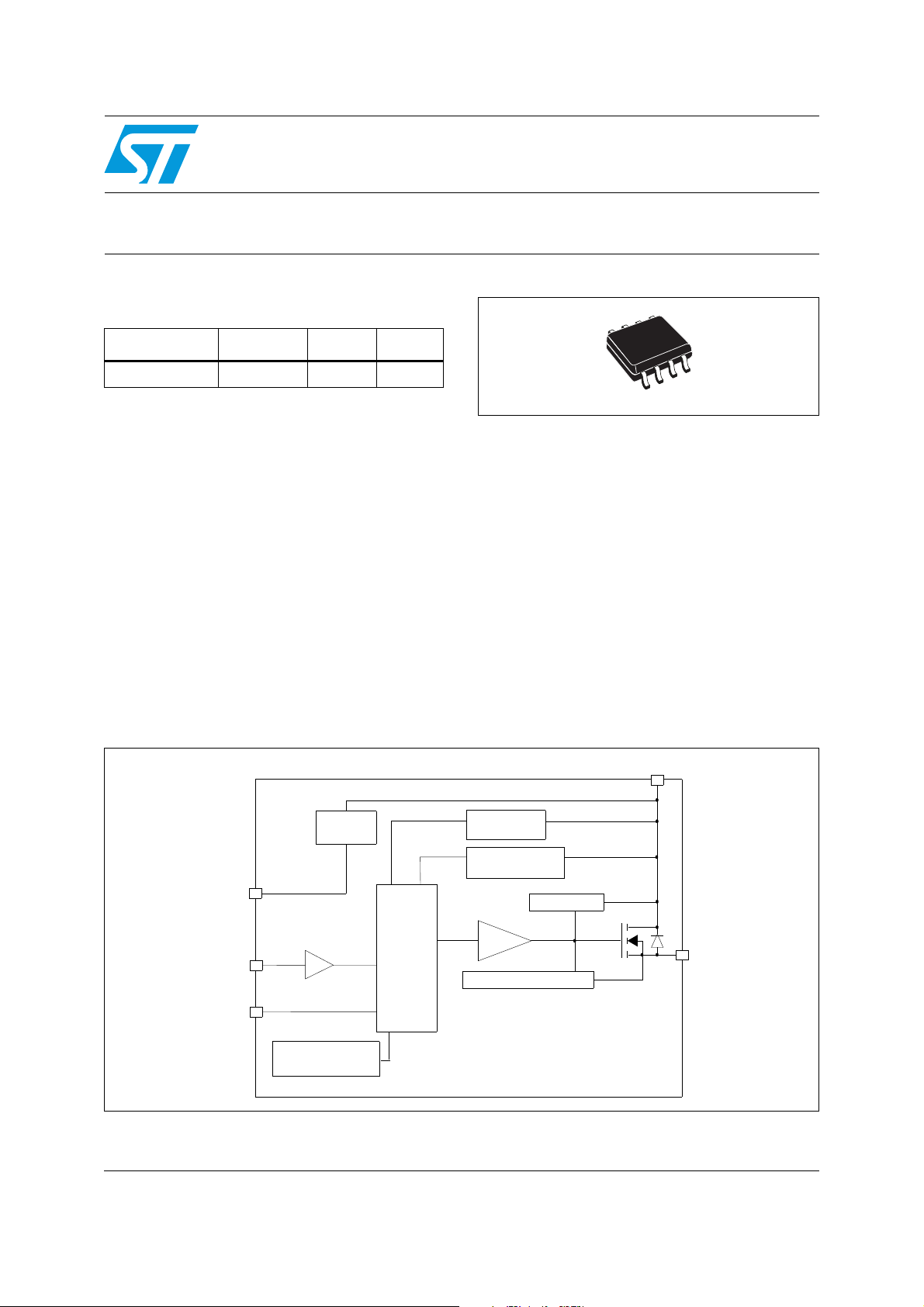
Figure 1. Block diagram
SO-8
Description
The VN751S is a monolithic device designed in
STMicroelectronics VIPower M0-3 technology,
intended for driving any kind of load with one side
connected to ground. Active V
clamp protects the device against low energy
spikes. Active current limitation combined with
thermal shutdown and automatic restart protect
the device against overload. Device automatically
turns off in case of ground pin disconnection. This
device is especially suitable for industrial
applications in conformity with IEC 61131-2
programmable controllers international standard.
V
CC
pin voltage
CC
OVERVOLTAGE
DETECTION
UNDERVOLTAGE
DETECTION
Power CLAMP
DRIVER
CURRENT LIMITER
OUTPUT
GND
INPUT
STATUS
V
CC
CLAMP
OVERTEMPERATURE
DETECTION
LOGIC
November 2009 Doc ID 12320 Rev 7 1/17
www.st.com
17
Page 2

Contents VN751S
Contents
1 Maximum ratings . . . . . . . . . . . . . . . . . . . . . . . . . . . . . . . . . . . . . . . . . . . . 3
2 Pin connections . . . . . . . . . . . . . . . . . . . . . . . . . . . . . . . . . . . . . . . . . . . . . 4
3 Electrical characteristics . . . . . . . . . . . . . . . . . . . . . . . . . . . . . . . . . . . . . 5
4 Waveforms and truth table . . . . . . . . . . . . . . . . . . . . . . . . . . . . . . . . . . . . 7
5 Test circuit . . . . . . . . . . . . . . . . . . . . . . . . . . . . . . . . . . . . . . . . . . . . . . . . . 9
6 Application schematic . . . . . . . . . . . . . . . . . . . . . . . . . . . . . . . . . . . . . . 10
7 Reverse polarity protection . . . . . . . . . . . . . . . . . . . . . . . . . . . . . . . . . . 11
8 Package mechanical data . . . . . . . . . . . . . . . . . . . . . . . . . . . . . . . . . . . . 12
9 Order code . . . . . . . . . . . . . . . . . . . . . . . . . . . . . . . . . . . . . . . . . . . . . . . . 15
10 Revision history . . . . . . . . . . . . . . . . . . . . . . . . . . . . . . . . . . . . . . . . . . . 16
2/17 Doc ID 12320 Rev 7
Page 3

VN751S Maximum ratings
1 Maximum ratings
Table 1. Absolute maximum rating
Symbol Parameter Value Unit
V
- V
- I
I
- I
I
V
T
E
OUT
I
STAT
ESD
P
T
T
DC supply voltage (overvoltage protected) 45 V
CC
Reverse DC supply voltage -0.3 V
CC
DC reverse ground pin current -200 mA
GND
DC output current Internally limited A
Reverse DC output current -5 A
OUT
DC input current +/- 10 mA
IN
DC status current +/- 10 mA
Electrostatic discharge (R = 1.5 kΩ; C = 100 pF) 5000 V
Power dissipation TC = 25 °C
tot
Junction operating temperature Internally limited °C
J
Case operating temperature - 40 to 150 °C
c
Storage temperature - 55 to 150 °C
stg
Single-pulse avalanche energy 0.8 J
AS
Internally limited W
Table 2. Thermal data
Symbol Parameter Value Unit
(1)
R
R
1. When mounted on a standard single-sided FR-4 board with 0.5 cm2 of Cu (at least 35μm) thick connected
to all V
2. When mounted on a standard single-sided FR-4 board with 2 cm2 of Cu (at least 35μm) thick connected to
all V
Thermal resistance junction-ambient Max
thJA
Thermal resistance junction-case Max 15 °C/W
thJC
pins. Horizontal mounting and no artificial air flow.
CC
pins. Horizontal mounting and no artificial air flow.
CC
93
82
(2)
°C/W
°C/W
Doc ID 12320 Rev 7 3/17
Page 4
Pin connections VN751S
2 Pin connections
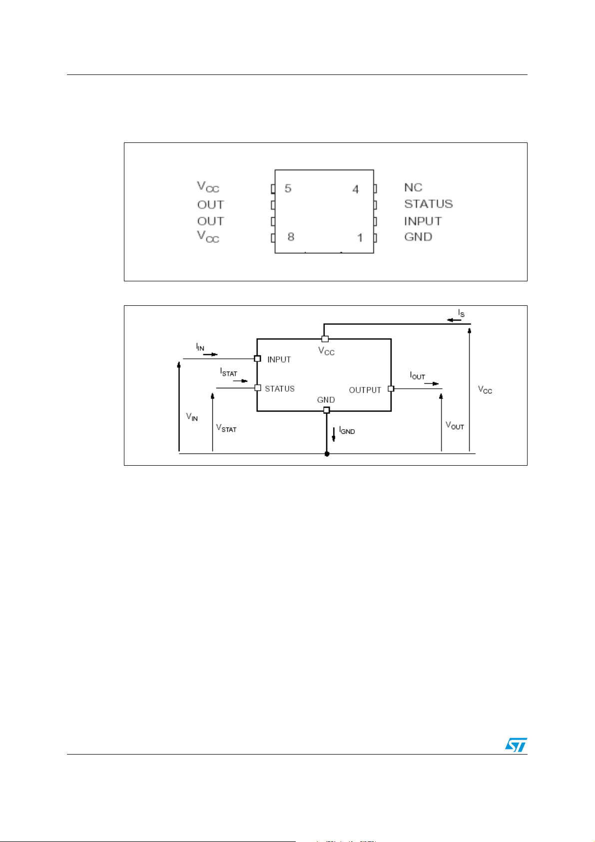
Figure 2. Connection diagram (top view)
Figure 3. Current and voltage conventions
4/17 Doc ID 12320 Rev 7
Page 5
VN751S Electrical characteristics
3 Electrical characteristics
8 V < V
< 36 V; -40 °C < TJ < 125 °C, unless otherwise specified
CC
Table 3. Power
Symbol Parameter Test conditions Min Typ Max Unit
V
V
V
R
I
L(off)
CC
USD
OV
ON
I
Operating supply
voltage
Undervoltage
shut-down
Overvoltage
shut-down
On state resistance
Supply current
S
Off state output current
I
= 2 A; TJ = 25 °C
OUT
= 2 A
I
OUT
Off state; V
On state; V
On state; V
= V
V
IN
OUT
= 24 V; T
CC
= 24 V
CC
= 24 V;T
CC
= 0 V
CASE
CASE
=25 °C
=100 °C
5.5 36 V
345.5V
36 V
60
180mΩmΩ
10
20
1.5
1.8
010μA
Table 4. Switching (VCC = 24 V)
Symbol Parameter Test conditions Min Typ Max Unit
μA
mA
mA
dV
dV
t
d(on)
t
d(off)
OUT
OUT
/dt
/dt
Turn-on delay time
Turn-off delay time
Turn -on voltage slope
(on)
Turn -off voltage slope
(off)
= 12 Ω from VIN rising edge to
R
L
V
= 2.4 V
OUT
= 12 Ω from VIN falling edge to
R
L
= 21.6 V
V
OUT
= 12Ω from V
R
L
= 19.2 V
V
OUT
= 12 Ω from V
R
L
= 2.4 V
V
OUT
= 2.4 V to
OUT
= 21.6 V to
OUT
12 μs
35 μs
0.80 V/μs
0.30 V/μs
Doc ID 12320 Rev 7 5/17
Page 6
Electrical characteristics VN751S
Table 5. Input pin
Symbol Parameter Test conditions Min Typ Max Unit
V
IL
I
IL
V
IH
I
IH
V
hyst
I
IN
V
ICL
Input low level 1.25 V
Low level input
current
V
= 1.25 V
IN
1 μA
Input high level 3.25 V
High level input
current
Input hysteresis
voltage
Input current
Input clamp voltage
V
= 3.25 V
IN
V
IN = VCC
I
= 1 mA
IN
= -1 mA
I
IN
= 5 V
0.5 V
6
6.8
-0.7
10 μA
10 μA
8 V
Table 6. Status pin
Symbol Parameter Test conditions Min Typ Max Unit
V
STAT
I
LSTAT
C
STAT
V
SCL
Status low output
voltage
Status leakage
current
Status pin input
capacitance
Status clamp voltage
I
= 1.6 mA
STAT
Normal operation; V
Normal operation; V
= 1 mA;
I
STAT
=-1 mA
I
STAT
STAT
STAT
= 5 V
= 5 V
6 6.8
-0.7
0.5 V
10 µA
100 pF
8 V
V
V
Table 7. Protections
Symbol Parameter Test conditions Min Typ Max Unit
T
TSD
T
R
T
hyst
I
lim
V
demag
6/17 Doc ID 12320 Rev 7
Shut-down
temperature
Reset temperature 135 °C
Thermal hysteresis 7 20 °C
Current limitation
CC
t = 0.4 ms
LOAD
V
= 24 V, R
Turn-off output
clamp
RL =12 Ω; L = 6 mH
voltage
= 10 mΩ,
150 175 200 °C
2.7 6.0 A
V
-47VCC-52VCC-
CC
57
V
Page 7

VN751S Waveforms and truth table
4 Waveforms and truth table
Figure 4. Switching time waveforms
V
OUT
t
d(off)
90%
dV
OUT
/dt
(off)
t
t
80%
/dt
dV
OUT
(on)
10%
V
IN
t
d(on)
Table 8. Truth table
Conditions Input Output Status
Normal operation
Current limitation
Overtemperature
Undervoltage
Overvoltage
L
H
L
H
H
L
H
L
H
L
H
L
H
L
X
X
L
L
L
L
L
L
(T
(T
< T
J
> T
J
TSD
TSD
H
H
H
) H
) L
H
L
X
X
H
H
Doc ID 12320 Rev 7 7/17
Page 8

Waveforms and truth table VN751S
Figure 5. Waveforms
NORMAL OPERATION
INPUT
LOAD VOLTAGE
STATUS
UNDERVOLTAGE
V
CC
V
USD
V
USDhyst
INPUT
LOAD VOLTAGE
STATUS
undefined
V
CC
INPUT
LOAD VOLTAGE
STATUS
T
J
INPUT
LOAD CURRENT
STATUS
T
T
TSD
R
V
CC<VOV
OVERVOLTAGE
VCC>V
OV
OVERTEMPERATURE
8/17 Doc ID 12320 Rev 7
Page 9

VN751S Test circuit
5 Test circuit
Figure 6. Peak short circuit current test circuit
R
Figure 7. Avalanche energy test circuit
R
Doc ID 12320 Rev 7 9/17
Page 10

Application schematic VN751S
6 Application schematic
Figure 8. Application schematic
10/17 Doc ID 12320 Rev 7
Page 11

VN751S Reverse polarity protection
7 Reverse polarity protection
A schematic solution to protect the IC against a reverse polarity condition is proposed.
This schematic is effective with any type of load connected to the outputs of the IC.
The RGND resistor value can be selected according to the following conditions to be met:
R
≤ 600 mV / (IS in ON state max).
GND
R
≥ (-VCC) / (-I
GND
where -IGND is the DC reverse ground pin current and can be found in the absolute
maximum rating section of the device datasheet.
GND
)
The power dissipation associated to R
PD = (-V
CC
)2/R
GND
during reverse polarity condition is:
GND
This resistor can be shared by several different ICs. In such case IS value on formula (1) is
the sum of the maximum ON-state currents of the different devices.
Please note that if the microprocessor ground and the device ground are separated then the
voltage drop across the R
(given by IS in ON state max * R
GND
) produce a difference
GND
between the generated input level and the IC input signal level. This voltage drop will vary
depending on how many devices are ON in the case of several high side switches sharing
the same R
GND
.
Figure 9. Reverse polarity protection
+ Vcc
+ Vcc
Status
Status
i
i
Output
Output
i
Input
Input
(Optional)
(Optional)
i
i
GND
R
R
GND
GND
GND
i
Load
Load
Doc ID 12320 Rev 7 11/17
Page 12

Package mechanical data VN751S
8 Package mechanical data
In order to meet environmental requirements, ST offers these devices in different grades of
ECOPACK
specifications, grade definitions and product status are available at: www.st.com.
ECOPACK is an ST trademark.
®
packages, depending on their level of environmental compliance. ECOPACK®
12/17 Doc ID 12320 Rev 7
Page 13

VN751S Package mechanical data
Table 9. SO-8 mechanical data
mm inch
Dim.
Min Typ Max Min Typ Max
A 1.75 0.068
a1 0.1 0.25 0.003 0.009
a2 1.65 0.064
a3 0.65 0.85 0.025 0.033
b 0.35 0.48 0.013 0.018
b1 0.19 0.25 0.007 0.010
C 0.25 0.5 0.010 0.019
c1 45 (typ.)
D 4.8 5.0 0.188 0.196
E 5.8 6.2 0.228 0.244
e 1.27 0.050
e3 3.81 0.150
F 3.8 4.0 0.14 0.157
L 0.4 1.27 0.015 0.050
M 0.6 0.023
S 8º (max.)
Figure 10. Package dimensions
Doc ID 12320 Rev 7 13/17
Page 14

Package mechanical data VN751S
Figure 11. SO-8 tape and reel information
14/17 Doc ID 12320 Rev 7
Page 15

VN751S Order code
9 Order code
Table 10. Order codes
Order codes Package Packaging
VN751S SO-8 Tube
VN751STR SO-8 tape and reel
Doc ID 12320 Rev 7 15/17
Page 16

Revision history VN751S
10 Revision history
Table 11. Document revision history
Date Revision Changes
18-Sep-2006 1 Initial release
12-Mar-2007 2
15-May-2007 3
18-Sep-2007 4
11-Oct-2007 5 Updated Table 2 on page 3
08-Jul-2008 6 Added Section 7 on page 10
30-Nov-2009 7 Updated coverpage and Chapter 6 on page 10
Document reformatted, typo in Section Table 3.: Power on
page 5, updated P
Typo in Table 1 on page 3 V
Added I
value in Table 1 on page 3
STAT
value Ta bl e 2
tot
.
ESD
16/17 Doc ID 12320 Rev 7
Page 17

VN751S
Please Read Carefully:
Information in this document is provided solely in connection with ST products. STMicroelectronics NV and its subsidiaries (“ST”) reserve the
right to make changes, corrections, modifications or improvements, to this document, and the products and services described herein at any
time, without notice.
All ST products are sold pursuant to ST’s terms and conditions of sale.
Purchasers are solely responsible for the choice, selection and use of the ST products and services described herein, and ST assumes no
liability whatsoever relating to the choice, selection or use of the ST products and services described herein.
No license, express or implied, by estoppel or otherwise, to any intellectual property rights is granted under this document. If any part of this
document refers to any third party products or services it shall not be deemed a license grant by ST for the use of such third party products
or services, or any intellectual property contained therein or considered as a warranty covering the use in any manner whatsoever of such
third party products or services or any intellectual property contained therein.
UNLESS OTHERWISE SET FORTH IN ST’S TERMS AND CONDITIONS OF SALE ST DISCLAIMS ANY EXPRESS OR IMPLIED
WARRANTY WITH RESPECT TO THE USE AND/OR SALE OF ST PRODUCTS INCLUDING WITHOUT LIMITATION IMPLIED
WARRANTIES OF MERCHANTABILITY, FITNESS FOR A PARTICULAR PURPOSE (AND THEIR EQUIVALENTS UNDER THE LAWS
OF ANY JURISDICTION), OR INFRINGEMENT OF ANY PATENT, COPYRIGHT OR OTHER INTELLECTUAL PROPERTY RIGHT.
UNLESS EXPRESSLY APPROVED IN WRITING BY AN AUTHORIZED ST REPRESENTATIVE, ST PRODUCTS ARE NOT
RECOMMENDED, AUTHORIZED OR WARRANTED FOR USE IN MILITARY, AIR CRAFT, SPACE, LIFE SAVING, OR LIFE SUSTAINING
APPLICATIONS, NOR IN PRODUCTS OR SYSTEMS WHERE FAILURE OR MALFUNCTION MAY RESULT IN PERSONAL INJURY,
DEATH, OR SEVERE PROPERTY OR ENVIRONMENTAL DAMAGE. ST PRODUCTS WHICH ARE NOT SPECIFIED AS "AUTOMOTIVE
GRADE" MAY ONLY BE USED IN AUTOMOTIVE APPLICATIONS AT USER’S OWN RISK.
Resale of ST products with provisions different from the statements and/or technical features set forth in this document shall immediately void
any warranty granted by ST for the ST product or service described herein and shall not create or extend in any manner whatsoever, any
liability of ST.
ST and the ST logo are trademarks or registered trademarks of ST in various countries.
Information in this document supersedes and replaces all information previously supplied.
The ST logo is a registered trademark of STMicroelectronics. All other names are the property of their respective owners.
© 2009 STMicroelectronics - All rights reserved
STMicroelectronics group of companies
Australia - Belgium - Brazil - Canada - China - Czech Republic - Finland - France - Germany - Hong Kong - India - Israel - Italy - Japan -
Malaysia - Malta - Morocco - Philippines - Singapore - Spain - Sweden - Switzerland - United Kingdom - United States of America
www.st.com
Doc ID 12320 Rev 7 17/17
 Loading...