

Page 1
October 1999 1/11
1
VN540 / VN540SP
/ VN540(011Y) / VN540(012Y)
HIGH SIDE SMART POWER SOLID STATE RELAY
1
■ OUTPUT CURRENT (CONTINUOUS): 2.8A
■ DIGITAL INPUT CLAMPED AT 32V
■ PROTECTION AGAINST: LOSS OF GROUND,
SHORTED LOAD AND OVERTEMPERATURE
■ BUILT-IN CURRENT LIMITER
■ UNDER VOLTAGE SHUT DOWN
■ OPEN DRAIN DIAGNOSTIC OUTPUT
■ FAST DEMAGNETIZATION OF INDUCTIVE
LOADS.
DESCRIPTION
The VN540, VN540SP, VN540(011Y),
VN540(012Y) is a monolithic device designed in
STMicroelectronics VIPower technology, intended
for driving resistive or inductive loads with one
side connected to ground. Active current limitation
avoids the system power supply dropping in case
of shorted load. Built-in thermal shut down
protects the chip from over temperature. Theopen
drain diagnostic output indicates over temperature
conditions.
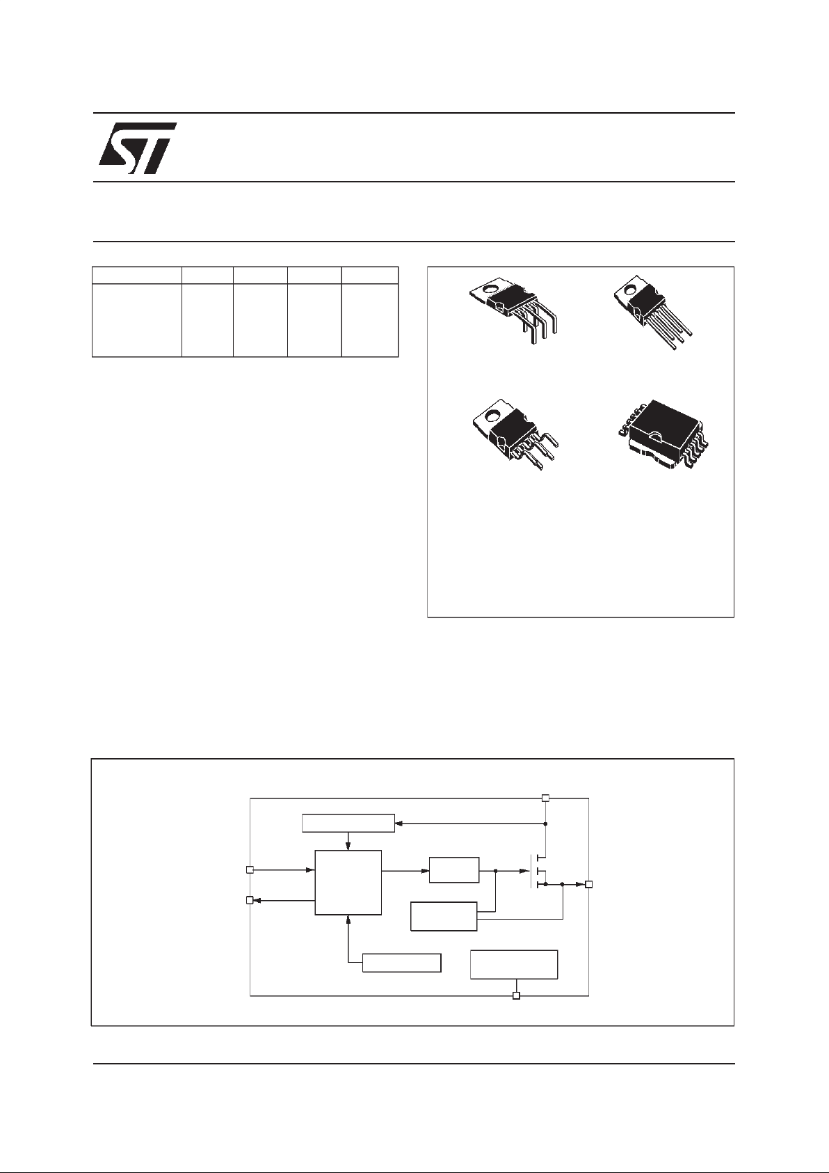
TYPE V
demagRDS(on)IOUT
V
CC
VN540
VN540SP
VN540(011Y)
VN540(012Y)
-55V 50mΩ 2.8A 36 V
PENTAWATT(011Y)
PENTAWATT
PowerSO-10
TM
1
10
PENTAWATT(012Y)
ORDER CODES
PENTAWATT vertical
PENTAWATT horizontal
PENTAWATT straight
PowerSO-10
TM
VN540
VN540(011Y)
VN540(012Y)
VN540SP
BLOCK DIAGRAM
DRIVER
CURRENT
OUTPUT
LIMITER
V
CC
NEGATIVE V
CC
PROTECTION
GROUND
CONTROL
LOGIC
OVERTEMP
UNDERVOLTAGE
STATUS
INPUT
Page 2
2/11
VN540 / VN540SP / VN540(011Y) / VN540(012Y)
ABSOLUTE MAXIMUM RATING
Symbol Parameter Value Unit
V
CC
Power supply voltage 45 V
-V
CC
Reverse supply voltage -4.0 V
I
OUT
Maximum DC load current Internally limited A
I
R
Reverse output current -10 A
I
IN
Input current +/- 10 mA
I
STAT
Status pin current +/- 10 mA
V
ESD
Electrostatic discharge (R=1.5kΩ, C=100pF) 2000 V
P
TOT
Power dissipation at Tc=25°C Internally limited W
T
j
Junction operating temperature Internally limited °C
T
STG
Storage temperature -55 to 150 °C
E
AS
Single pulse avalanche energy 500 mJ
1
CURRENT AND VOLTAGE CONVENTIONS
CONNECTION DIAGRAM TOP VIEW
1
2
3
4
5
6
7
8
9
10
11
OUTPUT
OUTPUT
N.C.
OUTPUT
OUTPUT
GROUND
INPUT
STATUS
N.C.
N.C.
V
CC
PowerSO-10
TM
PENTAWATT
Page 3
3/11
VN540 / VN540SP / VN540(011Y) / VN540(012Y)
THERMAL DATA
ELECTRICAL CHARACTERISTICS (10V<VCC<36V; -25°C<Tj<100°C; unless otherwisespecified)
POWER
SWITCHING
LOGIC INPUT
Symbol Parameter
Value
Unit
PowerSO-10 PENTAWATT
R
thj-case
Thermal resistance junction-case (MAX) 1.5 2.0 °C/W
R
thj-amb
Thermal resistance junction-ambient (MAX) 50 60 °C/W
Symbol Parameter Test Conditions Min Typ Max Unit
V
CC
Operating voltage 10 36 V
R
ON
On state resistance
I
OUT
=2.8A; Tj=25°C
I
OUT
=2.8A;
50
90
mΩ
mΩ
I
S
Supply current
OFF state
ON state (Tj=125°C)
I
OUT
=0A
1
3
mA
mA
I
LS
Output leakage current
Channel OFF
V
CC
=45V
100 µA
I
LGND
Output current at turn-off
V
CC=VIN=VGND=VSTAT
=24V
T
j
= -25°C<T
j
<100°C
2mA
V
OL
Low state output voltage VIN=VIL;R
LOAD
>10MΩ 1.5 V
V
demag
Output voltage at turn-off I
OUT
=2.8A; L
LOAD
=1mH VCC-65 VCC-55 VCC-45 V
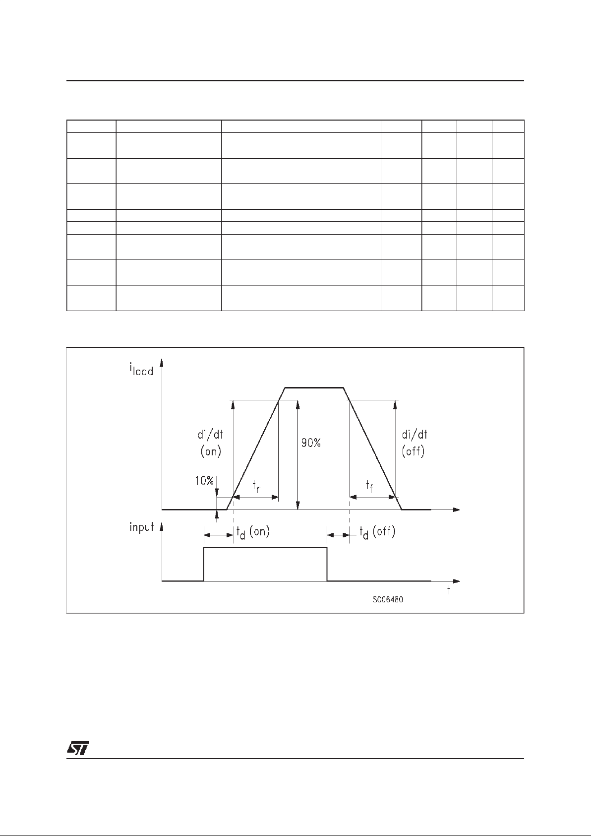
Symbol Parameter Test Conditions Min Typ Max Unit
t
d(on)
Turn-on delay on output
current
I
OUT
=2.8A; Resistive Load
Input rise time <0.1µs; V
CC
=24V;
T
j
=25°C
40 µs
t
r
Rise time of
output current
I
OUT
=2.8A; Resistive Load
Input rise time <0.1µs; V
CC
=24V;
T
j
=25°C
60 µs
t
d(off)
Turn-off delay on output
current
I
OUT
=2.8A; Resistive Load
Input rise time <0.1µs; V
CC
=24V;
T
j
=25°C
60 µs
t
f
Fall time of
output current
I
OUT
=2.8A; Resistive Load
Input rise time <0.1µs; V
CC
=24V;
T
j
=25°C
25 µs
dI/dt
(on)
Turn-on current average
slope
I
OUT
=2.8A
I
OUT=ILIM
;25°C<Tj<140°C
0.5
2
A/µs
A/µs
dI/dt
(off)
Turn-off current average
slope
I
OUT
=2.8A
I
OUT=ILIM
;25°C<Tj<140°C
2
4
A/µs
A/µs
Symbol Parameter Test Conditions Min Typ Max Unit
V
IL
Input low level voltage 2.0 V
V
IH
Input high level voltage 3.5 V
V
I(hyst)
Input hysteresis voltage 0.5 V
I
IN
Input current
V
IN
=30V
V
IN
=2.0V 25
300 µA
µA
V
ICL
Input clamp voltage
(see note 1)
IIN=1mA
I
IN
=-1mA
32 36
-0.7
V
V
1
Page 4
4/11
VN540 / VN540SP / VN540(011Y) / VN540(012Y)
PROTECTIONS AND DIAGNOSTICS
(*) Status determination > 100µs after the switching edge.
SWITCHING CHARACTERISTICS
Symbol Parameter Test Conditions Min Typ Max Unit
V
STAT
Status output voltage
I
STAT
=5mA
(Fault condition)
1V
V
SCL
(*)
Status clamp voltage I
STAT
=1mA
I
STAT
=-1mA
32 36
0.7
V
V
I
STAT
Leakage on diagnostic pin
in high state
V
STAT
=5V 10 µA
V
USD
Undervoltage shut-down 5.0 8.0 V
I
LIM
DC short circuit current VCC=24V, R
LOAD
<0.1Ω 2.8 5.0 8.0 A
t
SC
Delay time of
current limiter
100 µs
T
TSD
Thermal shut-down
temperature
150 170
o
C
T
R
Thermal reset
temperature
135 155
o
C
2
Note 1: The input voltage is internally clamped at 32V minimum, it is possible to connect the input pins to an higher voltage via an external
resistor calculate to not exceed 10mA.
Note 2: If INPUT pin is floating the corresponding channel will automatically switch off. If GND pin is disconnected, the channel will switch off
provided V
CC
not exceed 36V.
Page 5

5/11
VN540 / VN540SP / VN540(011Y) / VN540(012Y)
THRUTH TABLE
1
10kΩ
CONTROL
UNIT
R
IN
IN
GND
OUTPUT
R
L
<10mΩ
+V
CC
GND
STATUS
Fig. 1: Peak Short Test Circuit
INPUT OUTPUT STATUS
Normal operation L
H
L
H
H
H
Overtemperature L
H
L
L
H
L
Undervoltage L
H
L
L
H
H
Shorted load
(Current limitation)
L
H
L
H
H
H
Page 6

6/11
VN540 / VN540SP / VN540(011Y) / VN540(012Y)
2
Figure 2: Waveforms
A
+V
CC
OUT
STATUS
I/O1
GND
Fig. 3: I
LGND
Test Configuration
Page 7

7/11
VN540 / VN540SP / VN540(011Y) / VN540(012Y)
1
1
DIM.
mm. inch
MIN. TYP MAX. MIN. TYP. MAX.
A 3.35 3.65 0.132 0.144
A1 0.00 0.10 0.000 0.004
B 0.40 0.60 0.016 0.024
c 0.35 0.55 0.013 0.022
D 9.40 9.60 0.370 0.378
D1 7.40 7.60 0.291 0.300
E 9.30 9.50 0.366 0.374
E1 7.20 7.40 0.283 0.291
E2 7.20 7.60 0.283 300
E3 6.10 6.35 0.240 0.250
E4 5.90 6.10 0.232 0.240
e 1.27 0.050
F 1.25 1.35 0.049 0.053
H 13.80 14.40 0.543 0.567
h 0.50 0.002
Q 1.70 0.067
α 0º 8º
1
1
DETAIL ”A”
PLANE
SEATING
α
L
A1
F
A1
h
A
D
D1
==
==
==
E4
0.10 A
E1E3
C
Q
A
==
B
B
DETAIL”A”
SEATING
PLANE
==
==
E2
610
51
eB
HE
M
0.25
==
==
PowerSO-10 MECHANICAL DATA
Page 8

8/11
VN540 / VN540SP / VN540(011Y) / VN540(012Y)
1
DIM.
mm. inch
MIN. TYP MAX. MIN. TYP. MAX.
A 4.8 0.189
C 1.37 0.054
D 2.4 2.8 0.094 0.110
D1 1.2 1.35 0.047 0.053
E 0.35 0.55 0.014 0.022
F 0.8 1.05 0.031 0.041
F1 1 1.4 0.039 0.055
G 3.2 3.4 3.6 0.126 0.134 0.142
G1 6.6 6.8 7 0.260 0.268 0.276
H2 10.4 0.409
H3 10.05 10.4 0.396 0.409
L2 23.05 23.4 23.8 0.907 0.921 0.937
L3 25.3 25.65 26.1 0.996 1.010 1.028
L5 2.6 3 0.102 0.118
L6 15.1 15.8 0.594 0.622
L7 6 6.6 0.236 0.260
Diam. 3.65 3.85 0.144 0.152
PENTAWATT (IN-LINE) MECHANICAL DATA
Page 9

9/11
VN540 / VN540SP / VN540(011Y) / VN540(012Y)
DIM.
mm. inch
MIN. TYP MAX. MIN. TYP. MAX.
A 4.8 0.189
C 1.37 0.054
D 2.4 2.8 0.094 0.110
D1 1.2 1.35 0.047 0.053
E 0.35 0.55 0.014 0.022
F 0.8 1.05 0.031 0.041
F1 1 1.4 0.039 0.055
G 3.2 3.4 3.6 0.126 0.134 0.142
G1 6.6 6.8 7 0.260 0.268 0.276
H2 10.4 0.409
H3 10.05 10.4 0.396 0.409
L 14.2 15 0.559 0.590
L1 5.7 6.2 0.244
L2 14.6 15.2 0.598
L3 3.5 4.1 0.137 0.161
L5 2.6 3 0.102 0.118
L6 15.1 15.8 0.594 0.622
L7 6 6.6 0.236 0.260
Diam. 3.65 3.85 0.144 0.152
11
PENTAWATT (HORIZONTAL) MECHANICAL DATA
Page 10

10/11
VN540 / VN540SP / VN540(011Y) / VN540(012Y)
1
DIM.
mm. inch
MIN. TYP MAX. MIN. TYP. MAX.
A 4.8 0.189
C 1.37 0.054
D 2.4 2.8 0.094 0.110
D1 1.2 1.35 0.047 0.053
E 0.35 0.55 0.014 0.022
F 0.8 1.05 0.031 0.041
F1 1 1.4 0.039 0.055
G 3.2 3.4 3.6 0.126 0.134 0.142
G1 6.6 6.8 7 0.260 0.268 0.276
H2 10.4 0.409
H3 10.05 10.4 0.396 0.409
L 17.85 0.703
L1 15.75 0.620
L2 21.4 0.843
L3 22.5 0.886
L5 2.6 3 0.102 0.118
L6 15.1 15.8 0.594 0.622
L7 6 6.6 0.236 0.260
M 4.5 0.177
M1 4 0.157
Diam. 3.65 3.85 0.144 0.152
PENTAWATT (VERTICAL) MECHANICAL DATA
Page 11

11/11
VN540 / VN540SP / VN540(011Y) / VN540(012Y)
1
Information furnished is believed to be accurate and reliable. However, STMicroelectronics assumes no responsibility for the consequences
of use of such information nor for any infringement of patents or other rights of third parties which may results from its use. No license is
granted by implication or otherwise under any patent or patent rights of STMicroelectronics. Specifications mentioned in this publication are
subject to change without notice. This publication supersedes and replaces all information previously supplied. STMicroelectronics products
are not authorized for use as critical components in life support devices or systems without express written approval of STMicroelectronics.
The ST logo is a trademark of STMicroelectronics
1999 STMicroelectronics - Printed in ITALY-All Rights Reserved.
STMicroelectronics GROUP OF COMPANIES
Australia - Brazil - Canada - China - France - Germany - Italy - Japan - Korea - Malaysia - Malta - Mexico - Morocco -
The Netherlands - Singapore - Spain - Sweden - Switzerland - Taiwan - Thailand - United Kingdom - U.S.A.
http://www.st.com
 Loading...