

Page 1

DATA SH EET
Product specification
Supersedes data of 1998 Mar 03
File under Integrated Circuits, IC17
1998 Nov 19
INTEGRATED CIRCUITS
UMA1021AM
Low-voltage frequency synthesizer
for radio telephones
Page 2

1998 Nov 19 2
Philips Semiconductors Product specification
Low-voltage frequency synthesizer for
radio telephones
UMA1021AM
FEATURES
• Low phase noise
• Low current from 3 V supply
• Fully programmable main divider
• 3-line serial interface bus
• Independent fully programmable reference divider,
driven from external crystal oscillator
• Hard and soft power-down control.
APPLICATIONS
• 900 MHz and 2 GHz mobile telephones
• Portable battery-powered radio equipment.
GENERAL DESCRIPTION
The UMA1021AM BICMOS device integrates a prescaler,
programmable dividers, and a phase comparator to
implement a phase-locked loop.
The device is designed to operate from 3 NiCd cells, in
pocket phones, with low current and nominal 3 V supplies.
The synthesizer operates at RF input frequencies
up to 2.2 GHz with a fully programmable reference divider.
All divider ratios are supplied via a 3-wire serial
programming bus.
Separate power and ground pins are provided to the
analog (charge pump) and digital circuits. The ground
leads should be externally short-circuited to prevent large
currents flowing across the die and thus causing damage.
V
DD1
and V
DD2
must also be at the same potential (VDD).
VCC must be equal to or greater than VDD for wider control
range of the Voltage Controlled Oscillator (VCO),
e.g. VDD= 3 V and VCC=5V.
The charge pump current (phase detector gain) is fixed by
an external resistor at pin I
SET
and controlled via the serial
interface. Only a passive loop filter is necessary; the
charge pump functions within a wide voltage compliance
range to improve the overall system performance.
QUICK REFERENCE DATA
ORDERING INFORMATION
SYMBOL PARAMETER CONDITIONS MIN. TYP. MAX. UNIT
V
DD1
, V
DD2
digital supply voltage V
DD1=VDD2=VDD
2.7 − 5.5 V
V
CC
analog supply voltage for charge pump VCC≥ V
DD
2.7 − 5.5 V
I
tot
total supply current (IDD+ICC)V
CC=VDD
= 5.5 V − 10 − mA
I
tot(pd)
total supply current in Power-down
mode (IDD+ICC)
logic levels 0 V or V
DD
− 5 −µA
f
RF
RF input frequency 300 − 2200 MHz
f
xtal
crystal reference oscillator input
frequency
3 − 35 MHz
f
ph(comp)
phase comparator frequency − 200 − kHz
T
amb
operating ambient temperature −30 − +85 °C
TYPE NUMBER
PACKAGE
NAME DESCRIPTION VERSION
UMA1021AM SSOP16 plastic shrink small outline package; 16 leads; body width
4.4 mm
SOT369-1
Page 3
1998 Nov 19 3
Philips Semiconductors Product specification
Low-voltage frequency synthesizer for
radio telephones
UMA1021AM
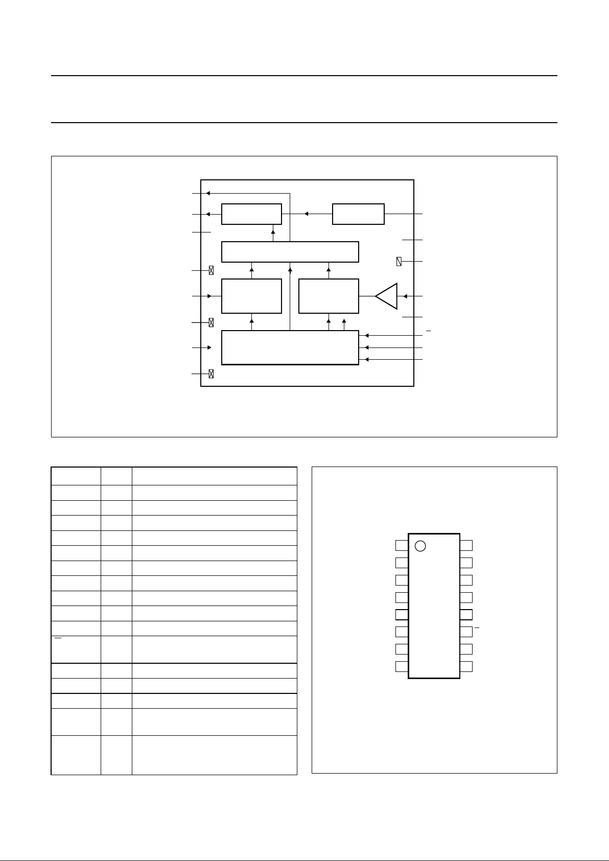
BLOCK DIAGRAM
Fig.1 Block diagram.
handbook, full pagewidth
MGL406
CHARGE PUMP
PHASE COMPARATOR
MAIN DIVIDER
WITH
PRESCALER
REFERENCE
DIVIDER
SERIAL INTERFACE
BAND GAP
2
3
1
5
7
11
10
9
13
16
UMA1021AM
CP
4
6
8
LOCK
V
SS3
RFI
V
SS2
V
DD2
PON
V
SS1
I
SET
XTAL
12
V
DD1
15
V
CC
14
GND(CP)
to charge pump
E
DATA
CLK
PINNING
SYMBOL PIN DESCRIPTION
LOCK 1 out-of-lock detector output
CP 2 charge pump output
V
DD2
3 digital supply voltage
V
SS3
4 ground 3 (0 V)
RFI 5 2 GHz main divider input
V
SS2
6 ground 2 (0 V)
PON 7 power-on input
V
SS1
8 ground 1 (0 V)
CLK 9 programming bus clock input
DATA 10 programming bus data input
E 11 programming bus enable input
(active LOW)
V
DD1
12 digital supply voltage
XTAL 13 crystal frequency input
GND(CP) 14 ground for charge pump
V
CC
15 analog supply voltage for charge
pump
I
SET
16 charge pump current setting with
external resistor from this pin to
ground
Fig.2 Pin configuration.
handbook, halfpage
UMA1021AM
MGL405
1
2
3
4
5
6
7
8
LOCK
CP
V
DD2
V
SS3
RFI
V
SS2
PON
V
SS1
I
SET
V
CC
GND(CP)
XTAL
V
DD1
E
DATA
CLK
16
15
14
13
12
11
10
9
Page 4

1998 Nov 19 4
Philips Semiconductors Product specification
Low-voltage frequency synthesizer for
radio telephones
UMA1021AM
FUNCTIONAL DESCRIPTION
Main divider
The main divider is clocked at pin RFI by the RF signal
which is AC-coupled from an external VCO. The divider
operates with signal levels from 50 to 225 mV (RMS) and
at frequencies from 300 MHz to 2.2 GHz. It consists of a
fully programmable bipolar prescaler followed by a CMOS
counter. The main divider allows programmable ratios
from 512 to 131071 inclusive.
Reference divider
The reference divider is clocked by the signal at pin XTAL.
The applied input signal should be AC-coupled. The circuit
operates with levels from 50 up to 500 mV (RMS) and at
frequencies from 3 to 35 MHz. Any divide ratios from
8 to 2047 inclusive can be programmed.
Phase comparator and charge pump
The phase detector is driven by the edges of the output
signals of the main and reference dividers. The detector
produces current pulses at pin CP. The pulse duration is
equal to the difference in time of arrival of the edges from
the two dividers. If the main divider edge arrives first,
pin CP sinks current. If the reference divider edge arrives
first, pin CP sources current.
The current at pin CP can be controlled via the serial
programming bus as a multiple of the reference current set
by an external pull-down resistor connected between
pin I
SET
and ground (see Table 2). Pin CP remains active
except in the Power-down mode.
Additional circuitry is included to ensure that the gain of the
phase detector remains linear even for small phase errors.
Out-of-lock detector
The out-of-lock detector is enabled or disabled via the
serial interface by setting bit OOL (dt12) HIGH or LOW
(see Table 1). An open-drain transistor drives the output
pin LOCK. It is recommended to keep the sink current in
the LOW state below 400 µA by applying a pull-up resistor
from pin LOCK to the positive supply. When the out-of-lock
detector is enabled pin LOCK is HIGH if the error at the
phase detector input is less than approximately 25 ns,
otherwise pin LOCK is LOW. If the out-of-lock detector is
disabled, pin LOCK remains HIGH.
Serial programming bus
A simple 3-line unidirectional serial bus is used to program
the circuit.
The 3 lines are DATA (data bits), CLK (clock pulses) and
E (enable signal). The data sent to the device is loaded in
bursts framed by E. Programming clock edges and their
appropriate data bits are ignored until E goes active LOW.
The programmed information is loaded into the addressed
latch when E returns HIGH. During normal operation,
E should be kept HIGH. Only the last 21 bits serially
clocked into the device are retained within the
programming register. Additional leading bits are ignored,
and no check is made on the number of clock pulses.
The fully static CMOS design uses virtually no current
when the programming bus is inactive. It can always
capture new programmed data even during power-down.
When the synthesizer is switched on, the presence of a
signal at the reference divider input is required for correct
programming.
Data format
The data format is shown in Table 1. The first bit entered
is dt16, the last bit is ad0.
The leading bits (dt16 to dt0) make up the data field.
The four trailing bits (ad3 to ad0) are the address field.
The UMA1021AM uses 4 of the 16 available addresses.
These are chosen for compatibility with other Philips
Semiconductors radio telephone ICs. The trailing address
bits are decoded on the rising edge of
E. This produces an
internal load pulse to store the data in the addressed latch.
To avoid erroneous divider ratios, the load pulse is not
allowed during data reads by the frequency dividers. This
condition is guaranteed by respecting a minimum E pulse
width after data transfer.
For the divider ratios, the first bits entered (PM16 and
PR10) are the Most Significant Bits (MSBs).
The test register (address 0000) does not normally need to
be programmed. However, if it is programmed all bits in the
data field should be set to logic 0.
Power-down mode
The synthesizer is switched on when both the power-on
input (PON) and the programmed bit dt6 (sPON) are
HIGH. When switched on, the dividers and phase detector
are synchronized to avoid random phase errors. When
switched off, the phase detector is synchronized to avoid
interrupting of the charge pump pulses.
The UMA1021AM has a very low current consumption in
the Power-down mode.
Page 5

1998 Nov 19 5
Philips Semiconductors Product specification
Low-voltage frequency synthesizer for
radio telephones
UMA1021AM
This text is here in white to force landscape pages to be rotated correctly when browsing through the pdf in the Acrobat reader.This text is here in
_white to force landscape pages to be rotated correctly when browsing through the pdf in the Acrobat reader.This text is here inThis text is here in
white to force landscape pages to be rotated correctly when browsing through the pdf in the Acrobat reader. white to force landscape pages to be ...
Table 1 Bit allocation; note 1
Notes
1. X = don’t care.
2. The test register (address 0000) should not be programmed with any other values except all zeros for normal operation.
3. Bit OOL sets the Out-Of-Lock detector (1 = enabled).
4. Bits CR1 and CR0 set the charge pump current ratio (see Table 2).
5. Bit sPON sets the software power-up for the synthesizer (see Table 3).
6. PM16 is the MSB of the main divider coefficient.
7. PR10 is the MSB of the reference divider coefficient.
FIRST IN REGISTER BIT ALLOCATION LAST IN
DATA FIELD ADDRESS
dt16 dt15 dt14 dt13 dt12 dt11 dt10 dt9 dt8 dt7 dt6 dt5 dt4 dt3 dt2 dt1 dt0 ad3 ad2 ad1 ad0
test bits; note 2 0 0 0 0
X X X X OOL
(3)
X CR1
(4)
CR0 X X sPON
(5)
XXXXX X 0 0 0 1
PM16
(6)
main divider coefficient PM0 0 1 0 0
X X X X X X PR10
(7)
reference divider coefficient PR0 0 1 0 1
Table 2 Charge pump current ratio; note 1
Note
1. Reference current for charge pump:
BIT CR1 BIT CR0
CHARGE PUMP
CURRENT
0010×I
set
0118×I
set
1013×I
set
1117×I
set
I
set
V
set
R
set
---------- -
=
Table 3 Power-on programming
Notes
1. Signal level
a) L = LOW.
b) X = don’t care.
c) H = HIGH.
2. X = don’t care.
PIN PON
(1)
BIT sPON
(2)
SYNTHESIZER
STATE
L X off
X 0 off
H1on
Page 6

1998 Nov 19 6
Philips Semiconductors Product specification
Low-voltage frequency synthesizer for
radio telephones
UMA1021AM
LIMITING VALUES
In accordance with the Absolute Maximum Rating System (IEC 134).
HANDLING
All pins withstand the ESD class 2 test in accordance with
“EIA/JESD22-A114-A”
.
THERMAL CHARACTERISTICS
SYMBOL PARAMETER CONDITIONS MIN. MAX. UNIT
V
DD1
, V
DD2
digital supply voltage −0.3 +5.5 V
V
CC
analog supply voltage for charge pump −0.3 +5.5 V
∆V
CC-DD
supply voltage difference
between the analog and digital supply
voltages
−0.3 +5.5 V
V
n
voltage
at pins 5, 7, 9, 10 and 11 −0.3 V
DD
+ 0.3 V
at pins 1, 2, 13 and 16 −0.3 V
CC
+ 0.3 V
∆V
GND
difference in voltage between any of
pins GND(CP), V
SS1
, V
SS2
and V
SS3
these pins should be
connected together
−0.3 +0.3 V
P
tot
total power dissipation − 85 mW
T
stg
storage temperature −55 +125 °C
T
amb
operating ambient temperature −30 +85 °C
T
j(max)
maximum junction temperature − 150 °C
SYMBOL PARAMETER CONDITIONS VALUE UNIT
R
th(j-a)
thermal resistance from junction to ambient in free air 142 K/W
Page 7

1998 Nov 19 7
Philips Semiconductors Product specification
Low-voltage frequency synthesizer for
radio telephones
UMA1021AM
CHARACTERISTICS
All values refer to the typical test and application diagram of Fig.5; V
DD1=VDD2
= 2.7 to 5.5 V; VCC= 2.7 to 5.5 V;
T
amb
=25°C; unless otherwise specified. Characteristics for which only a typical value is given are not tested.
SYMBOL PARAMETER CONDITIONS MIN. TYP. MAX. UNIT
Supplies; pins 3, 12 and 15
V
DD1
, V
DD2
digital supply voltage V
DD1=VDD2=VDD
2.7 − 5.5 V
V
CC
analog supply voltage for charge
pump
VCC≥ V
DD
2.7 − 5.5 V
I
DD
total digital supply current of
synthesizer (I
DD1+IDD2
)
VDD= 5.5 V − 7 9.5 mA
I
CC
analog supply current of charge
pump
VCC= 5.5 V;
R
set
= 5.6 kΩ
− 3 3.8 mA
I
tot(pd)
total supply current in
Power-down mode (IDD+ICC)
logic levels0VorVDD− 550µA
RF main divider input; pin 5
f
RF
RF input frequency 300 − 2200 MHz
V
RF(rms)
input signal level (RMS value) AC-coupled; series
resistance Rs=50Ω
50 − 225 mV
D/D
m
main divider ratio 512 − 131071
Z
i
input impedance (real part) fRF= 1 GHz − 750 −Ω
f
RF
= 2 GHz − 130 −Ω
C
i
input capacitance fRF= 1 GHz − 0.5 − pF
f
RF
= 2 GHz − 1.5 − pF
Reference divider input; pin 13
f
xtal
crystal reference oscillator input
frequency
3 − 35 MHz
V
xtal(rms)
sinusoidal input signal level
(RMS value)
50 − 500 mV
D/D
ref
reference divider ratio 8 2047
Z
i
input impedance (real part) f
xtal
=13MHz − 10 − kΩ
C
i
input capacitance f
xtal
=13MHz − 1.3 − pF
Phase comparator
f
ph(comp)
phase comparator frequency − 200 − kHz
f
loop(max)
maximum loop comparison
frequency
− 2000 − kHz
Charge pump current setting; pin 16
R
set
external resistor connected between
pin 16 and ground
5.6 − 12 kΩ
V
set
regulated voltage R
set
= 5.6 kΩ−1.2 − V
Page 8

1998 Nov 19 8
Philips Semiconductors Product specification
Low-voltage frequency synthesizer for
radio telephones
UMA1021AM
Charge pump output; pin 2
V
o(compl)
compliance output voltage R
set
= 5.6 kΩ 0.4 − VCC− 0.4 V
I
o(err)
output current error R
set
= 5.6 kΩ−25 − +25 %
I
o(match)
sink-to-source current matching R
set
= 5.6 kΩ−±5−%
I
L
leakage current R
set
= 5.6 kΩ;
charge pump off;
V
o(compl)
=1⁄2V
CC
−5 ±1+5 nA
Phase noise
N
900
RF synthesizer’s contribution to
close-in phase noise of 900 MHz
VCO signal inside the closed loop
bandwidth
f
xtal
= 13 MHz;
V
xtal
= 0 dBm;
f
ph(comp)
= 200 kHz
−−88 −
dBc/Hz
N
1800
RF synthesizer’s contribution to
close-in phase noise of 1.8 GHz
VCO signal inside the closed loop
bandwidth
f
xtal
= 13 MHz;
V
xtal
= 0 dBm;
f
ph(comp)
= 200 kHz
−−82 −
dBc/Hz
Interface logic inputs; pins 7, 9, 10 and 11
V
IH
HIGH-level input voltage 0.7V
DD
− VDD+ 0.3 V
V
IL
LOW-level input voltage −0.3 − 0.3V
DD
V
I
i(bias)
input bias current logic 1 or logic 0 −5 − +5 µA
C
i
input capacitance − 2 − pF
Out-of-lock detector output; pin 1
V
OL
LOW-level output voltage open-drain output −−0.3V
DD
V
E
ϕ(th)
threshold phase error open-drain output − 25 − ns
SYMBOL PARAMETER CONDITIONS MIN. TYP. MAX. UNIT
Page 9

1998 Nov 19 9
Philips Semiconductors Product specification
Low-voltage frequency synthesizer for
radio telephones
UMA1021AM
SERIAL BUS TIMING CHARACTERISTICS
V
DD1=VDD2=VCC
=3V; T
amb
=25°C; unless otherwise specified.
Note
1. The minimum pulse width (t
W
) can be smaller than 4000 ns when the both conditions are fulfilled:
a) Main divider input frequency:
b) Reference divider input frequency:
SYMBOL PARAMETER CONDITIONS MIN. TYP. MAX. UNIT
Serial programming clock; CLK
t
r
rise time − 10 40 ns
t
f
fall time − 10 40 ns
T
cy
clock cycle time 100 −−ns
Enable programming;
E
t
START
delay to rising clock edge 40 −−ns
t
END
delay from last falling clock edge −20 −−ns
t
W
minimum inactive pulse width note 1 4000 −−ns
t
SU;E
enable set-up time to next clock edge 20 −−ns
Register serial input data; DATA
t
SU;DAT
input data to clock set-up time 20 −−ns
t
HD;DAT
input data to clock hold time 20 −−ns
f
RF
447
t
W
--------- -
>
f
xtal
3
t
W
----- -
>
Fig.3 Serial bus timing diagram.
handbook, full pagewidth
MBG368
MSB LSB ADDRESS
t
START
t
SU;DAT
t
HD;DAT
T
cy
t
r
t
f
t
W
t
ENDtSU;E
CLK
DATA
E
Page 10

1998 Nov 19 10
Philips Semiconductors Product specification
Low-voltage frequency synthesizer for
radio telephones
UMA1021AM
APPLICATION INFORMATION
Fig.4 Typical application block diagram.
handbook, full pagewidth
MGL407
MAIN
DIVIDER
REFERENCE
DIVIDER
PHASE
COMPARATOR
AND
CHARGE PUMP
UMA1021AM
TCXO
SPLITTER VCO LPF
PLL
power
amplifier
low noise
amplifier
duplex
filter
transmit
data
transmit
mixer
to demodulation
1st mixer 2nd mixer
Page 11

1998 Nov 19 11
Philips Semiconductors Product specification
Low-voltage frequency synthesizer for
radio telephones
UMA1021AM
Fig.5 Typical test and application diagram.
(1) Values depend on application.
handbook, full pagewidth
MGL408
UMA1021AM
16
15
14
13
12
11
10
9
1
LOCK
I
SET
V
CC
GND(CP)
XTAL
V
DD1
E
DATA
CLK
CP
V
DD2
V
SS3
RFI
V
SS2
PON
V
SS1
2
3
4
5
6
7
8
12 Ω
56 pF
56 Ω
1 kΩ
18 Ω
to 1st mixer
18 Ω
56 pF
1 nF
18 Ω
(1)
(1)
(1)(1)
(1)
positive supply
control
out
RF VCO
100
nF
4.7
µF
100 nF
12 Ω
positive supply
12 Ω 12 Ω 12 Ω
3-wire bus
100 nF
1 nF
f
osc
V
CC
GND V
control
VTCXO
100 nF
12 Ω
12 Ω
5.6 kΩ
12 Ω
positive supply
100 nF
Page 12

1998 Nov 19 12
Philips Semiconductors Product specification
Low-voltage frequency synthesizer for
radio telephones
UMA1021AM
PACKAGE OUTLINE
UNIT A1A2A
3
b
p
cD
(1)E(1)
(1)
eHELLpQZywv θ
REFERENCES
OUTLINE
VERSION
EUROPEAN
PROJECTION
ISSUE DATE
IEC JEDEC EIAJ
mm
0.15
0.00
1.4
1.2
0.32
0.20
0.25
0.13
5.30
5.10
4.5
4.3
0.65
6.6
6.2
0.65
0.45
0.48
0.18
10
0
o
o
0.130.2 0.1
DIMENSIONS (mm are the original dimensions)
Note
1. Plastic or metal protrusions of 0.20 mm maximum per side are not included.
0.75
0.45
1.0
SOT369-1
94-04-20
95-02-04
w M
θ
A
A
1
A
2
b
p
D
y
H
E
L
p
Q
detail X
E
Z
e
c
L
v M
A
X
(A )
3
A
0.25
18
16
9
pin 1 index
0 2.5 5 mm
scale
SSOP16: plastic shrink small outline package; 16 leads; body width 4.4 mm
SOT369-1
A
max.
1.5
Page 13

1998 Nov 19 13
Philips Semiconductors Product specification
Low-voltage frequency synthesizer for
radio telephones
UMA1021AM
SOLDERING
Introduction
There is no soldering method that is ideal for all IC
packages. Wave soldering is often preferred when
through-hole and surface mounted components are mixed
on one printed-circuit board. However, wave soldering is
not always suitable for surface mounted ICs, or for
printed-circuits with high population densities. In these
situations reflow soldering is often used.
This text gives a very brief insight to a complex technology.
A more in-depth account of soldering ICs can be found in
our
“Data Handbook IC26; Integrated Circuit Packages”
(order code 9398 652 90011).
Reflow soldering
Reflow soldering techniques are suitable for all SSOP
packages.
Reflow soldering requires solder paste (a suspension of
fine solder particles, flux and binding agent) to be applied
to the printed-circuit board by screen printing, stencilling or
pressure-syringe dispensing before package placement.
Several techniques exist for reflowing; for example,
thermal conduction by heated belt. Dwell times vary
between 50 and 300 seconds depending on heating
method. Typical reflow temperatures range from
215 to 250 °C.
Preheating is necessary to dry the paste and evaporate
the binding agent. Preheating duration: 45 minutes at
45 °C.
Wave soldering
Wave soldering is not recommended for SSOP packages.
This is because of the likelihood of solder bridging due to
closely-spaced leads and the possibility of incomplete
solder penetration in multi-lead devices.
If wave soldering cannot be avoided, the following
conditions must be observed:
• A double-wave (a turbulent wave with high upward
pressure followed by a smooth laminar wave)
soldering technique should be used.
• The longitudinal axis of the package footprint must
be parallel to the solder flow and must incorporate
solder thieves at the downstream end.
Even with these conditions, only consider wave
soldering SSOP packages that have a body width of
4.4 mm, that is SSOP16 (SOT369-1) or
SSOP20 (SOT266-1).
During placement and before soldering, the package must
be fixed with a droplet of adhesive. The adhesive can be
applied by screen printing, pin transfer or syringe
dispensing. The package can be soldered after the
adhesive is cured.
Maximum permissible solder temperature is 260 °C, and
maximum duration of package immersion in solder is
10 seconds, if cooled to less than 150 °C within
6 seconds. Typical dwell time is 4 seconds at 250 °C.
A mildly-activated flux will eliminate the need for removal
of corrosive residues in most applications.
Repairing soldered joints
Fix the component by first soldering two diagonallyopposite end leads. Use only a low voltage soldering iron
(less than 24 V) applied to the flat part of the lead. Contact
time must be limited to 10 seconds at up to 300 °C. When
using a dedicated tool, all other leads can be soldered in
one operation within 2 to 5 seconds between
270 and 320 °C.
Page 14

1998 Nov 19 14
Philips Semiconductors Product specification
Low-voltage frequency synthesizer for
radio telephones
UMA1021AM
DEFINITIONS
LIFE SUPPORT APPLICATIONS
These products are not designed for use in life support appliances, devices, or systems where malfunction of these
products can reasonably be expected to result in personal injury. Philips customers using or selling these products for
use in such applications do so at their own risk and agree to fully indemnify Philips for any damages resulting from such
improper use or sale.
Data sheet status
Objective specification This data sheet contains target or goal specifications for product development.
Preliminary specification This data sheet contains preliminary data; supplementary data may be published later.
Product specification This data sheet contains final product specifications.
Limiting values
Limiting values given are in accordance with the Absolute Maximum Rating System (IEC 134). Stress above one or
more of the limiting values may cause permanent damage to the device. These are stress ratings only and operation
of the device at these or at any other conditions above those given in the Characteristics sections of the specification
is not implied. Exposure to limiting values for extended periods may affect device reliability.
Application information
Where application information is given, it is advisory and does not form part of the specification.
Page 15

1998 Nov 19 15
Philips Semiconductors Product specification
Low-voltage frequency synthesizer for
radio telephones
UMA1021AM
NOTES
Page 16

Internet: http://www.semiconductors.philips.com
Philips Semiconductors – a worldwide company
© Philips Electronics N.V. 1998 SCA60
All rights are reserved. Reproduction in whole or in part is prohibited without the prior written consent of the copyright owner.
The information presented in this document does not form part of any quotation or contract, is believed to be accurate and reliable and may be changed
without notice. No liability will be accepted by the publisher for any consequence of its use. Publication thereof does not convey nor imply any license
under patent- or other industrial or intellectual property rights.
Middle East: see Italy
Netherlands: Postbus 90050, 5600 PB EINDHOVEN, Bldg. VB,
Tel. +31 40 27 82785, Fax. +31 40 27 88399
New Zealand: 2 Wagener Place, C.P.O. Box 1041, AUCKLAND,
Tel. +64 9 849 4160, Fax. +64 9 849 7811
Norway: Box 1, Manglerud 0612, OSLO,
Tel. +47 22 74 8000, Fax. +47 22 74 8341
Pakistan: see Singapore
Philippines: Philips Semiconductors Philippines Inc.,
106 Valero St. Salcedo Village, P.O. Box 2108 MCC, MAKATI,
Metro MANILA, Tel. +63 2 816 6380, Fax. +63 2 817 3474
Poland: Ul. Lukiska 10, PL 04-123 WARSZAWA,
Tel. +48 22 612 2831, Fax. +48 22 612 2327
Portugal: see Spain
Romania: see Italy
Russia: Philips Russia, Ul. Usatcheva 35A, 119048 MOSCOW,
Tel. +7 095 755 6918, Fax. +7 095 755 6919
Singapore: Lorong 1, Toa Payoh, SINGAPORE 319762,
Tel. +65 350 2538, Fax. +65 251 6500
Slovakia: see Austria
Slovenia: see Italy
South Africa: S.A. PHILIPS Pty Ltd., 195-215 Main Road Martindale,
2092 JOHANNESBURG, P.O. Box 7430 Johannesburg 2000,
Tel. +27 11 470 5911, Fax. +27 11 470 5494
South America: Al. Vicente Pinzon, 173, 6th floor,
04547-130 SÃO PAULO, SP, Brazil,
Tel. +55 11 821 2333, Fax. +55 11 821 2382
Spain: Balmes 22, 08007 BARCELONA,
Tel. +34 93 301 6312, Fax. +34 93 301 4107
Sweden: Kottbygatan 7, Akalla, S-16485 STOCKHOLM,
Tel. +46 8 5985 2000, Fax. +46 8 5985 2745
Switzerland: Allmendstrasse 140, CH-8027 ZÜRICH,
Tel. +41 1 488 2741 Fax. +41 1 488 3263
Taiwan: Philips Semiconductors, 6F, No. 96, Chien Kuo N. Rd., Sec. 1,
TAIPEI, Taiwan Tel. +886 2 2134 2865, Fax. +886 2 2134 2874
Thailand: PHILIPS ELECTRONICS (THAILAND) Ltd.,
209/2 Sanpavuth-Bangna Road Prakanong, BANGKOK 10260,
Tel. +66 2 745 4090, Fax. +66 2 398 0793
Turkey: Talatpasa Cad. No. 5, 80640 GÜLTEPE/ISTANBUL,
Tel. +90 212 279 2770, Fax. +90 212 282 6707
Ukraine: PHILIPS UKRAINE, 4 Patrice Lumumba str., Building B, Floor 7,
252042 KIEV, Tel. +380 44 264 2776, Fax. +380 44 268 0461
United Kingdom: Philips Semiconductors Ltd., 276 Bath Road, Hayes,
MIDDLESEX UB3 5BX, Tel. +44 181 730 5000, Fax. +44 181 754 8421
United States: 811 East Arques Avenue, SUNNYVALE, CA 94088-3409,
Tel. +1 800 234 7381
Uruguay: see South America
Vietnam: see Singapore
Yugoslavia: PHILIPS, Trg N. Pasica 5/v, 11000 BEOGRAD,
Tel. +381 11 625 344, Fax.+381 11 635 777
For all other countries apply to: Philips Semiconductors,
International Marketing & Sales Communications, Building BE-p, P.O. Box 218,
5600 MD EINDHOVEN, The Netherlands, Fax. +31 40 27 24825
Argentina: see South America
Australia: 34 Waterloo Road, NORTH RYDE, NSW 2113,
Tel. +61 2 9805 4455, Fax. +61 2 9805 4466
Austria: Computerstr. 6, A-1101 WIEN, P.O. Box 213, Tel. +43 160 1010,
Fax. +43 160 101 1210
Belarus: Hotel Minsk Business Center, Bld. 3, r. 1211, Volodarski Str. 6,
220050 MINSK, Tel. +375 172 200 733, Fax. +375 172 200 773
Belgium: see The Netherlands
Brazil: seeSouth America
Bulgaria: Philips Bulgaria Ltd., Energoproject, 15thfloor,
51 James Bourchier Blvd., 1407 SOFIA,
Tel. +359 2 689 211, Fax. +359 2 689 102
Canada: PHILIPS SEMICONDUCTORS/COMPONENTS,
Tel. +1 800 234 7381
China/Hong Kong: 501 Hong Kong Industrial Technology Centre,
72 Tat Chee Avenue, Kowloon Tong, HONG KONG,
Tel. +852 2319 7888, Fax. +852 2319 7700
Colombia: see South America
Czech Republic: see Austria
Denmark: Prags Boulevard 80, PB 1919, DK-2300 COPENHAGEN S,
Tel. +45 32 88 2636, Fax. +45 31 57 0044
Finland: Sinikalliontie 3, FIN-02630 ESPOO,
Tel. +358 9 615800, Fax. +358 9 61580920
France: 51 Rue Carnot, BP317, 92156 SURESNES Cedex,
Tel. +33 1 40 99 6161, Fax. +33 1 40 99 6427
Germany: Hammerbrookstraße 69, D-20097 HAMBURG,
Tel. +49 40 23 53 60, Fax. +49 40 23 536 300
Greece: No. 15, 25th March Street, GR 17778 TAVROS/ATHENS,
Tel. +30 1 4894 339/239, Fax. +30 1 4814 240
Hungary: seeAustria
India: Philips INDIA Ltd, Band Box Building, 2nd floor,
254-D, Dr. Annie Besant Road, Worli, MUMBAI 400 025,
Tel. +91 22 493 8541, Fax. +91 22 493 0966
Indonesia: PT Philips Development Corporation, Semiconductors Division,
Gedung Philips, Jl. Buncit Raya Kav.99-100, JAKARTA 12510,
Tel. +62 21 794 0040 ext. 2501, Fax. +62 21 794 0080
Ireland: Newstead, Clonskeagh, DUBLIN 14,
Tel. +353 1 7640 000, Fax. +353 1 7640 200
Israel: RAPAC Electronics, 7 Kehilat Saloniki St, PO Box 18053,
TEL AVIV 61180, Tel. +972 3 645 0444, Fax. +972 3 649 1007
Italy: PHILIPS SEMICONDUCTORS, Piazza IV Novembre 3,
20124 MILANO, Tel. +39 2 6752 2531, Fax. +39 2 6752 2557
Japan: Philips Bldg 13-37, Kohnan 2-chome, Minato-ku,
TOKYO 108-8507, Tel. +81 3 3740 5130, Fax. +81 3 3740 5077
Korea: Philips House, 260-199 Itaewon-dong, Yongsan-ku, SEOUL,
Tel. +82 2 709 1412, Fax. +82 2 709 1415
Malaysia: No. 76 Jalan Universiti, 46200 PETALING JAYA, SELANGOR,
Tel. +60 3 750 5214, Fax. +60 3 757 4880
Mexico: 5900 Gateway East, Suite 200, EL PASO, TEXAS 79905,
Tel. +9-5 800 234 7381
Printed in The Netherlands 435102/750/02/pp16 Date of release: 1998 Nov 19 Document order number: 9397 750 04261
 Loading...