

Page 1

INTEGRATED CIRCUITS
DATA SH EET
UMA1002
Data processor for cellular radio
(DPROC2)
Product specification
Supersedes data of 1996 Sep 13
File under Integrated Circuits, IC17
1997 Jan 28
Page 2
Philips Semiconductors Product specification
Data processor for cellular radio
(DPROC2)
FEATURES
• Single chip solution to all the data handling and
supervisory functions
• Configuration to both AMPS and TACS
• Additional JTACS option
• I2C-bus serial control
• All analog interface and filtering functions fully
implemented on chip
• Error handling in hardware reduces software
requirements
• Robust SAT decoding and transponding circuitry
• Low current consumption by on-chip power-down
modes
• Reduced system current consumption by new
integrated power-saving features
– Majority voting includes more intelligence
– On-chip control filler word filter
– BCH error filter
– Possibility to program ESCC bits
• Small physical size: SO28 or LQFP32
• External peripheral component count reduced
– On-chip selectable clock divider
– Integrated pull-up resistor at TXLINE
• Simplified reset and abort software routines possible
• The SO28 version is fully compatible with UMA1000LT
and UMF1000T.
UMA1002
GENERAL DESCRIPTION
The UMA1002 is a low power CMOS LSI device
incorporating the data transceiving, data processing, and
SAT functions (including on-chip filtering) for an AMPS or
TACS hand-held portable cellular radio telephone.
In this data sheet, the UMA1002 is often referred to by the
descriptive term ‘DPROC2’.
QUICK REFERENCE DATA
SYMBOL PARAMETER MIN. TYP. MAX. UNIT
V
DD
I
DD
T
amb
ORDERING INFORMATION
TYPE
NUMBER
UMA1002T SO28 plastic small outline package; 28 leads; body width 7.5 mm SOT136-1
UMA1002H LQFP32 plastic low profile quad flat package; 32 leads; body 7 × 7 × 1.4 mm SOT358-1
1997 Jan 28 2
supply voltage 2.7 3.0 5.5 V
supply current normal operation with external clock − 1.3 1.8 mA
operating ambient temperature −30 − +70 °C
PACKAGE
NAME DESCRIPTION VERSION
Page 3

1997 Jan 28 3
b
ook, full pagewidth
BLOCK DIAGRAM
(DPROC2)
V
DDAVDDD INVRX RECDATA MVO
Philips Semiconductors Product specification
Data processor for cellular radio
DEMODD
AGND
DATA
RESET
3
ANTI-
ALIASING
(31)
FILTER
UMA1002
2 (30)
4
(32)
6
RESET, CLOCK AND
POWER-DOWN
(2)
GENERATOR
(3)10 (8)7 (4)28 (27)(28)
COMPARATOR 1
DATA
RECOVERY
SAT
FILTER
CLOCK
FILTER
12 (10)(20)
13 (11)
CLKOUTCLKINCLKSEL
INTERPOLATOR
BIAS
GENERATOR
OUTPUT
FILTER
TEST
LOGIC
9
(7)22(22)
TST TSCAN
COMPARATOR 2
GATED D/A
GATED D/A
1 (29)
SSA
SAT
RECOVERY
SAT
REGENERATION
ST
GENERATOR
14 (12)
V
SSD
SYNCRONIZATION
AND VOTING
DOTTING
DETECTOR
SAT
DETERMINATION
MANCHESTER
AND BCH
ENCODING
(6) 21 (21)
ERROR
CORECTION
ARBITRATION
LOGIC
TRANSMIT
BUFFER
2
I C
INTERFACE
23
(23)
A0INVTXJTACSV
8 (5)
27 (26)
19 (17)
5 (1)
20 (19)
11 (9)
18 (16)
17 (15)
15 (13)
25 (25)
24 (24)
RXLINE
RXCLK
BUSY/VSAT
RACTRL
TXCTRL
TACTRL
TXCLK
TXHOLD
TXLINE
SCL
SDA
MBD827
Pins in parenthesis apply to UMA1002H in LQFP32.
UMA1002
Fig.1 Block diagram.
Page 4

Philips Semiconductors Product specification
Data processor for cellular radio
UMA1002
(DPROC2)
PINNING
SYMBOL
V
SSA
AGND 2 30 Internally generated analog signal ground. V oltage level =
DEMODD 3 31 DEMODD inputs analog data and SAT signals from the RF demodulator. This pin
DA TA 4 32 Data is an analog output which provides the Manchester encoded and filtered data
RACTRL 5 1 Received audio control output. Open-drain output used to blank the audio path to
RESET 6 2 Master reset input resetting all internal flip-flops to the specified state. This input
INVRX 7 4 This input inverts the sense of received data stream, which allows RF
RXLINE 8 5 Received data signal output to the system controller.
TST 9 7 Test input pin (note 1).
RECDATA 10 8 Output of the recovered digital data signal (note 1).
TACTRL 11 9 Transmitter audio control output. This open-drain output is used to blank the audio
CLKIN 12 10 1.2 MHz or 9.6 MHz external master clock input. This input signal should be
CLKOUT 13 11 Output of 1.2 MHz clock signal (for APROC) derived from CLKIN.
V
SSD
TXLINE 15 13 Open-drain bidirectional data line to the system controller (internal 100 kΩ pull-up).
n.c. 16 14 Not connected.
TXHOLD 17 15 This input holds off transmission of data when set to HIGH.
TXCLK 18 16 Transmitted data clock input from the system controller.
BUSY/VSA T 19 17 Output indicating the status of the RECC by providing output information based on
PIN
DESCRIPTION
SO28 LQFP32
1 29 Negative analog supply (0 V). To be connected low-ohmic to V
1
.
SSD
⁄2V
. This pin should
DDA
be connected to a blocking capacitor, no DC load allowed.
should normally be AC-coupled. See Chapter “AC characteristics”.
signal, SAT and signalling tone. This signal should normally be AC-coupled into the
Audio/Data summer. See Chapter “AC characteristics”.
the earpiece when a sequence of dotting followed by a synchronization word or 2
synchronization words separated by 77 bits is detected. RACTRL and TACTRL
functions can be combined using one line. Output level LOW means audio muted.
has no influence on analog parts, but must be controlled by an active HIGH
microcontroller port.
demodulators with high or low local oscillators to be used. The AMPS and TACS
specifications define NRZ encoded logic 1 as a LOW-to-HIGH transition in the
centre of a data bit period. The polarity of the demodulated data stream into
DPROC2 depends on the receiver local oscillator. Input LOW means data normal.
path and enable the data path to the modulator during data bursts on the RVC.
Output level LOW means audio muted.
accurate to 100 × 10
−6
and have a worst case 60 : 40 mark-space ratio.
14 12 Negative digital supply (0 V), internally connected to substrate. To be connected
low-ohmic to V
SSA
.
a majority decision on the last 3 consecutive Busy/Idle bits (FVC = logic 0). Output
level LOW means channel idle.
Indicating the result of the comparison of the measured SA T and the expected SAT
colour-code bits (I
2
C-bus register) in the voice channel mode (FVC = logic 1 and
ENSM = logic 1). Output level LOW means incoming SAT not equal to expected
SAT.
1997 Jan 28 4
Page 5

Philips Semiconductors Product specification
Data processor for cellular radio
UMA1002
(DPROC2)
SYMBOL
TXCTRL 20 19 Transmitter control open-drain output used to disable the transmitter during an
INVTX 21 21 This input inverts the sense of transmitted data stream, which allows RF
TSCAN 22 22 Test switch input, only enabled if TST = logic 1, but should have a defined state.
A0 23 23 Input to select the least significant bit of the I
SDA 24 24 Serial data input/output (I
SCL 25 25 Serial clock input (I
n.c. 26 18 Not connected.
RXCLK 27 26 Received data clock input from the system controller.
V
DDD
V
DDA
MVO − 3 Majority voting output indicating that on FOCC the first 3 received words do not
JTACS − 6 Digital input signal for JTACS, input HIGH means that data is routed from TXLINE
CLKSEL − 20 Input switch for internal divide-by-8 or divide-by-1 divider between CLKIN and
PIN
SO28 LQFP32
RECC access failure. Output level LOW means RF disabled.
modulators with high or low local oscillators to be used. The AMPS and TACS
specifications define NRZ encoded logic 1 as a LOW-to-HIGH transition in the
centre of a data bit period. The polarity of the modulated data stream depends on
the transmitter local oscillator. Input LOW means data inverted.
2
C-bus).
28 27 Digital supply voltage (+3 V).
− 28 Analog supply voltage (+3 V).
differ from each other and thus the majority decision over 5 words can already be
carried out. Because of the required speed, indication is at this pin (and not via the
2
I
C-bus) which can be monitored by the system controller. Output LOW means the
receiver can be switched off.
directly without processing to gated D/A converter (if enabled by STEN bit).
CLKOUT (internal pull-down → divide-by-1 is default if not bonded out in SO28
package).
2
C-bus).
DESCRIPTION
2
C-bus address.
Note
1. Must not be connected in existing applications.
1997 Jan 28 5
Page 6
Philips Semiconductors Product specification
Data processor for cellular radio
(DPROC2)
handbook, halfpage
V
SSA
AGND
DEMODD
DATA
RACTRL
RESET
INVRX
RXLINE
TST
RECDATA
TACTRL
CLKIN
CLKOUT
V
SSD
1
2
3
4
5
6
7
8
9
10
11
12
13
UMA1002T
MBD828
V
28
DDD
27
RXCLK
n.c.
26
25
SCL
24
SDA
23
A0
22
TSCAN
21
INVTX
20
TXCTRL
19
BUSY/VSAT
18
TXCLK
17
TXHOLD
16
n.c.
1514
TXLINE
UMA1002
handbook, full pagewidth
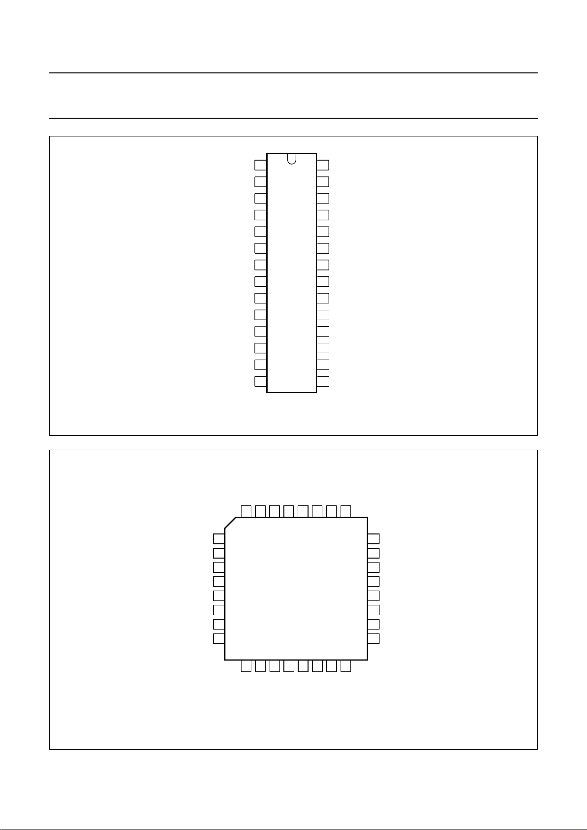
Fig.2 Pin configuration for SO28, SOT136-1.
SSA
DDA
SSD
DDD
V
28
27
13
14
n.c.
TXLINE
RACTRL
RESET
MVO
INVRX
RXLINE
JTACS
TST
RECDATA
DATA
AGNDVV
DEMODD
32
31
30
29
1
2
3
4
5
6
7
8
9
10
CLKIN
TACTRL
UMA1002H
11
12
V
CLKOUT
RXCLK
SCL
26
25
15
16
TXCLK
TXHOLD
24
SDA
23
A0
22
TSCAN
INVTX
21
20
CLKSEL
19
TXCTRL
18
n.c.
BUSY/VSAT
17
MBD829
Fig.3 Pin configuration for LQFP32, SOT358-1.
1997 Jan 28 6
Page 7

Philips Semiconductors Product specification
Data processor for cellular radio
(DPROC2)
FUNCTIONAL DESCRIPTION
General
The UMA1002 (DPROC2) is a single-chip CMOS device
which handles the data and supervisory functions of an
AMPS or TACS subscriber set.
These functions are:
• Data reception and transmission
• Control and voice channel exchanges
• Error detection, correction, decoding and encoding
• Supervisory Audio Tone decoding and transponding
• Signalling Tone generation.
In an AMPS or TACS cellular telephone system, mobile
stations communicate with a base over full duplex RF
channels. A call is initially set up using one out of a number
of dedicated control channels. This establishes a duplex
voice connection using a pair of voice channels.
Any further transmission of control data occurs on these
voice channels by briefly blanking the audio and
simultaneously transmitting the data. The data burst is
brief and barely noticeable by the user. A data rate of
10 kbits/s is used in the AMPS system and 8 kbits/s in
TACS. The signalling formats for both Forward Channels
(base to mobile) and Reverse Channels (mobile to base)
are shown in Fig.14.
A function known as Supervisory Audio Tone (SAT), a set
of 3 audio tones (5970, 6000 and 6030 Hz), is used to
indicate the presence of the mobile on the designated
voice channel. This signal, which is analogous to the
On-Hook signal on land lines, is sent out to the mobile by
the base station on the Forward Voice Channel. The signal
must be accurately recovered and transponded back to
the base station to complete the ‘loop’. At the base station
this signal is used to ascertain the overall quality of the
communication link.
Another voice channel associated signal is Signalling
Tone (ST). This tone (8 kHz TACS, 10 kHz AMPS) is
generated by the mobile and is sent in conjunction with
SAT on the Reverse Voice Channel to serve as an
acknowledgement signal to a number of system orders.
The key requirements of a hand-held portable cellular set
are:
• Small physical size
• Minimum number of interconnections (serial bus)
• Low power consumption
• Low cost.
UMA1002
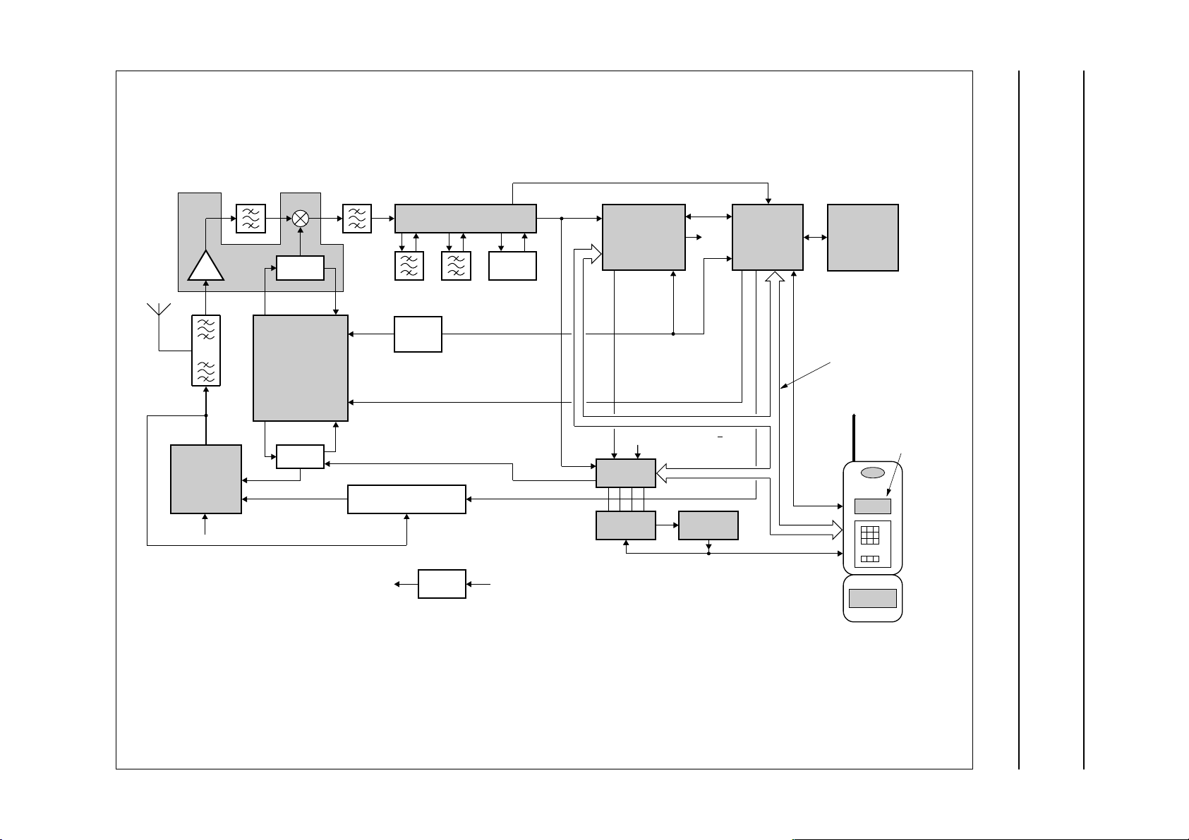
The DPROC2 is a member of our Cellular Radio chip set,
based on the I
A cellular radio system schematic using the chip set is
shown in Fig.11.
DPROC2 power-saving features
To support current saving in the application, DPROC2 has
three different modes of circuit operation implemented.
They are decoded by the I
activity on the data transfer link (TXCLK and TXLINE).
In power-down mode the relevant digital circuits have the
clock disabled, the analog circuits have the bias currents
and the switched capacitor clock switched off.
• Normal mode: all circuit parts are operating (e.g. on
Voice channels)
• Power-down mode 1: the SAT path is in power-down
(e.g. during access of the RECC)
• Power-down mode 2: the SAT path and the total data
transmit path are in power-down (e.g. for Idle state,
DPROC2 operating only on FOCC).
System power-saving features
Besides the above mentioned power-down modes
DPROC2 also includes features to reduce system current
(e.g. switching off parts of the receiver, and put the system
controller into Idle mode for longer periods of time).
All these features are controlled by the I
explanation of the following features refer to the Section
“I2C-bus serial data link (SDA; SCL)” sub-section “I2C-bus
registers”.
M
AJORITY VOTING (ONLY IN LQFP32)
Majority voting includes more intelligence. This feature is
enabled in FOCC with I2C-bus bit MAJ = logic 1.
If 3 consecutive identical words have been received it is
signalled via pin MVO. Therefore during the last 2 frame
words the receiver could be switched off to save system
current consumption.
C
ONTROL FILLER WORDS FILTER
System current can be further reduced by an on-chip
control filler words filter in FOCC, which enables the
detection of consecutive identical control filler words.
If consecutive control filler words are identical (i.e. DCC,
CMAC and WFOM) they will not be passed on to the
microcontroller. Consequently the system controller can
remain in power-saving mode.
2
C-bus, which meets these requirements.
2
C-bus register bit FVC and by
2
C-bus. For further
1997 Jan 28 7
Page 8
Philips Semiconductors Product specification
Data processor for cellular radio
(DPROC2)
PROGRAMMING OF ESCC BITS
There is a possibility to program the expected ESCC bits,
so that DPROC2 can compare expected and received
SAT and signal any inconsistency to the system controller
via BUSY/VSAT pin. Consequently there is no need to
read the measured SAT periodically via the I2C-bus.
BCH
ERROR FILTER
If this feature is enabled, DPROC2 will not pass on to the
microcontroller words with BCH errors. Consequently the
microcontroller can remain in power-saving mode. This
feature in combination with the control filler feature is
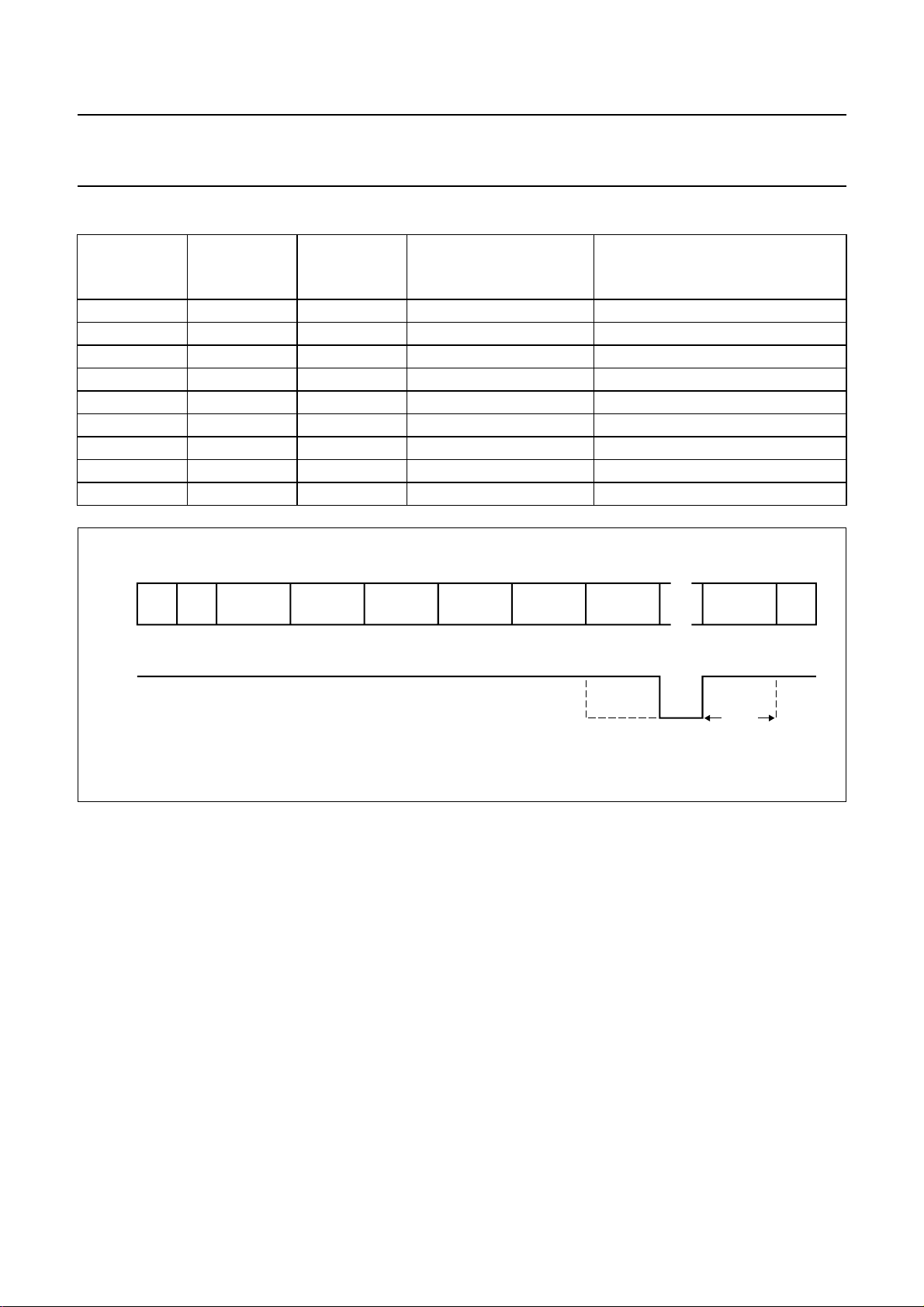
defined in Table 8.
S
ELECTABLE CLOCK DIVIDER (ONLY IN LQFP32)
An on-chip selectable divide-by-8 clock divider reduces
external peripheral component count.
UMA1002
Power-up state and master reset (RESET)
RESET should be HIGH as soon as power supply is
available.
DPROC2 will not respond reliably to any inputs (including
RESET) until 100 µs after the power supply has settled
within the specified tolerance. The analog sections of the
device will have stabilized within 5 ms. No on-chip
power-on reset is provided, therefore before the device
can enter normal operation RESET must be held HIGH.
RESET is an active HIGH master reset input, with a
minimum active pulse width of 4 µs which may be used to
reset the total logic within DPROC2 to a predefined state
as illustrated in Tables 1 and 2. It is preferably only used
during power-up, during normal operation it is
recommended to use the fully synchronous reset signals
derived from the I2C-bus bits FVC, STS and TXRST
(see Table 4). To ensure correct operation TXCLK must
be held HIGH during RESET operation.
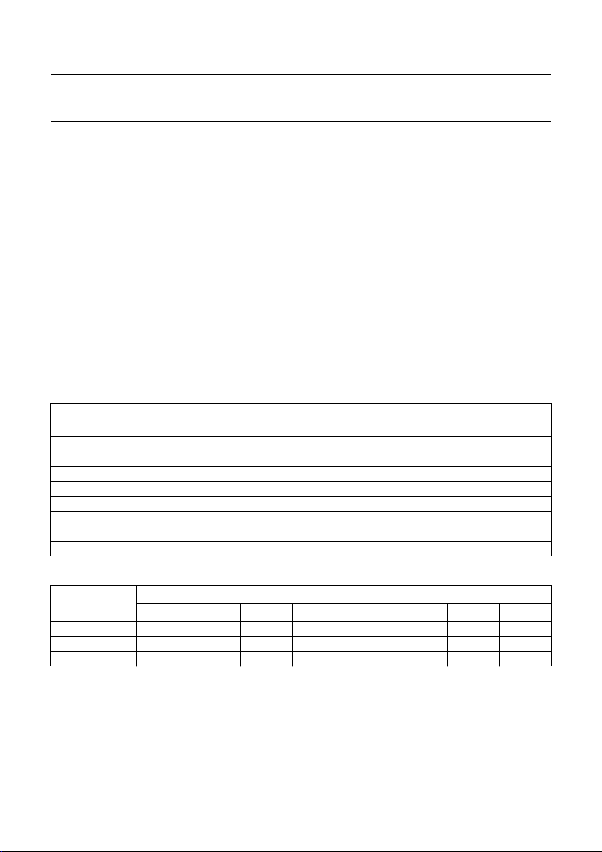
Table 1 Predefined state of the digital output pins
OUTPUT STATE
RXLINE HIGH
TXCTRL high-impedance (HIGH)
TACTRL high-impedance (HIGH)
RACTRL high-impedance (HIGH)
BUSY/VSAT HIGH
TXLINE HIGH (by 100 kΩ internal pull-up resistor)
RECDATA LOW
MVO HIGH
SDA high-impedance (HIGH)
2
Table 2 Predefined state of the I
REGISTER
76543210
Status (read) LOW LOW LOW HIGH LOW LOW HIGH HIGH
Control 1 (write) LOW LOW LOW LOW LOW LOW LOW LOW
Control 2 (write) LOW LOW LOW LOW LOW LOW LOW LOW
C-bus registers
BIT
1997 Jan 28 8
Page 9
Philips Semiconductors Product specification
Data processor for cellular radio
(DPROC2)
I2C-bus serial data link (SDA; SCL)
SDA is the bidirectional data line, SCL is the clock input
from an I2C-bus master. These constitute a typical I2C link
and conform to standard I2C-bus characteristics.
A detailed description of the I2C-bus specification, with
applications, is given in the brochure
how to use it”.
This brochure may be ordered using the
code 9398 393 40011.
• Data rate up to 100 kbits/s.
S
LAVE ADDRESS SELECT (A0)
Selection of the device slave address is achieved by
connecting A0 to either VSS or V
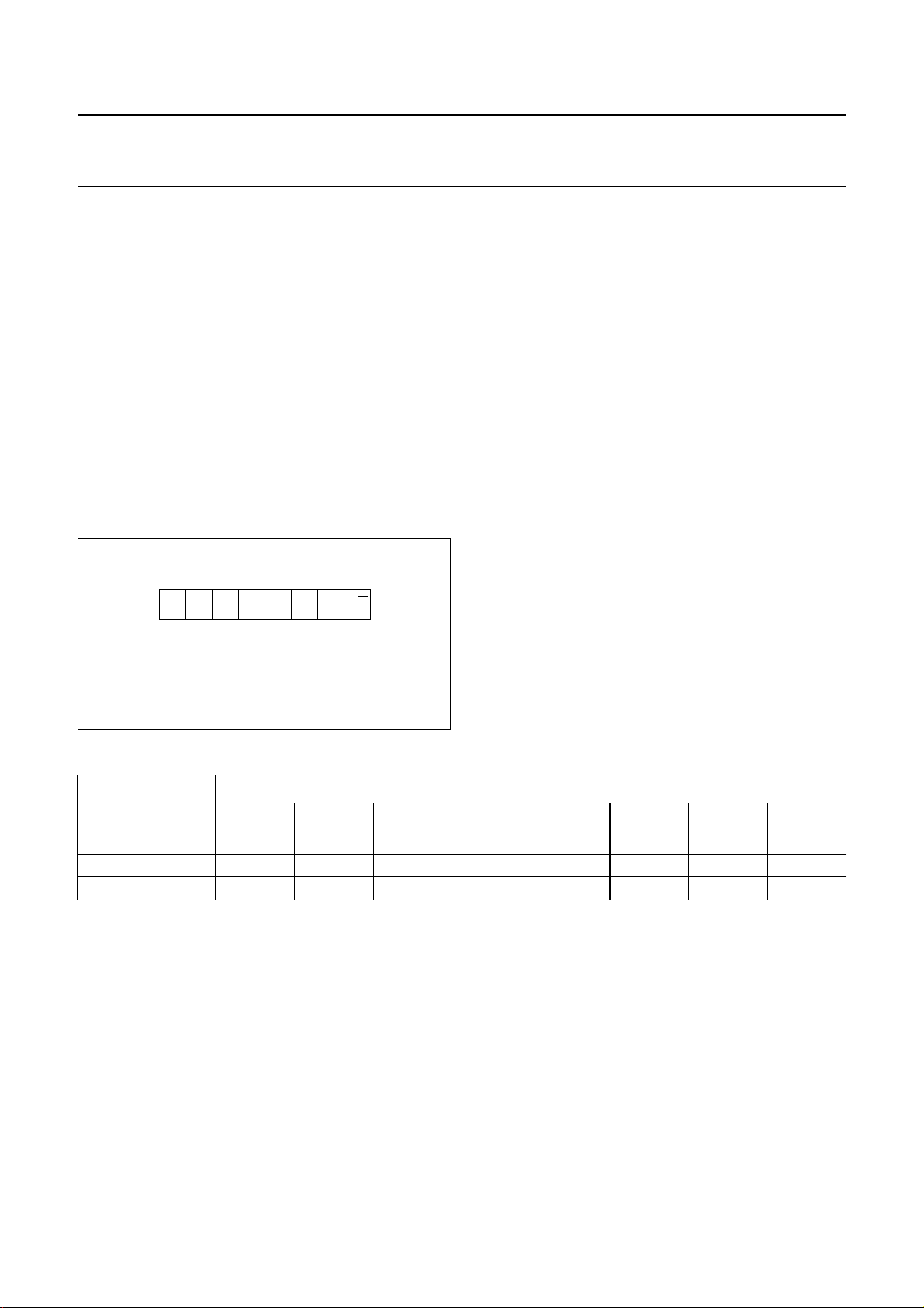
defined in accordance with the I2C-bus specifications as
shown in Fig.4.
handbook, halfpage
“The I2C-bus and
. The slave address is
DDD
(1)
R/W11011XA0
MBD831
UMA1002
I2C-BUS REGISTERS
The I2C-bus register block resides internally within the
I2C-bus interface block and contains various items of
status and control information which are transferred to and
from DPROC2 via the I2C-bus. The block is organized into
three 8-bit registers:
• Status register which contains read only items
• Control registers 1 and 2 which contain write only items.
(1) X = don’t care.
Fig.4 Device slave address.
Table 3 I2C-bus register map
BIT
REGISTER
76543210
Status (read) −−WSYNC BUSY TXABRT TXIP MSCC1 MSCC0
Control 1 (write) BUFEN SERV STS TXRST ABREN FVC STEN SATEN
Control 2 (write) MAJ MR1 MR0 DBCH DCFM ENSM ESCC1 ESCC0
1997 Jan 28 9
Page 10

Philips Semiconductors Product specification
Data processor for cellular radio
(DPROC2)
handbook, full pagewidth
(a) Read from DPROC2 status register.
(b) Write to DPROC2 control register 1.
(c) Write to all DPROC2 control registers.
Where:
S = START condition
W = read/write bit (logic 0 = write)
R = read/write bit (logic 1 = read)
A = acknowledge bit
P = STOP condition
DPROC ADR = slave address of DPROC2.
DPROC ADRS R A STATUS
P
(a)
WA APDPROC ADRS
CONTROL 1
(b)
WA ADPROC ADRS CONTROL 2 A P
CONTROL 1
MBD832
(c)
UMA1002
Fig.5 I2C-bus data format.
1997 Jan 28 10
Page 11

Philips Semiconductors Product specification
Data processor for cellular radio
UMA1002
(DPROC2)
Table 4 Description of I2C-bus register map
REGISTER
BITS
Control Register 1
BUFEN 0 1.2 MHz signal not available at pin CLKOUT
SERV 0 serving system data stream B selected
(1)
STS
TXRST 1 terminates a message being transmitted on the reverse channel; monostable
ABREN 1 DPROC2 has permission to abort data transmission and disable RF on the RECC
(2)
FVC
STEN 0 disables output of signalling tone to pin DATA
SATEN 0 disables output of SAT transponded signal to pin DATA
LOGIC LEVEL DESCRIPTION
1 1.2 MHz signal is available at pin CLKOUT
1 serving system data stream A selected
0 TACS selected
1 AMPS selected
signal causing a reset of the message transmission circuitry and resets the
I2C-bus bits TXABRT, TXIP and clears the transmit buffer
following the detection of a channel access attempt collision
0 no permission for above operations
0 control channel format selected
1 voice channel format selected
1 enables output of signalling tone to pin DATA if FVC = logic 1
1 enables output of SAT transponded signal to pin DATA if FVC = logic 1
Control Register 2
MAJ 0 majority voting procedure on FOCC using all 5 frame words, MVO output is always
HIGH
1 majority voting procedure on FOCC using the first 3 frame words, if they are all
identical the MVO pin goes LOW (see Fig.6)
MR0, MR1 see Table 5 determines set-up time of MVO signal with respect to beginning of the next dotting
(see Fig.6)
DBCH see Table 8 BCH error filter
DCFM see Table 8 control filler message filter
ENSM 0 enable SAT monitoring; ESCC bits are not used
1 enable SAT monitoring; ESCC bits are used for following function
ESCC0,
ESCC1
Status Register
WSYNC 0 DPROC2 has not acquired frame synchronization in accordance with FOCC
see Table 6 expected SAT colour code bits; the incoming SAT is compared to these bits, the
result (expected or not expected SAT frequency) is given out by the BUSY/VSAT
pin (when FVC = logic 1), which prevents periodical reading from the I
status register
format
1 DPROC2 has acquired frame synchronization in accordance with FOCC format
2
C-bus
1997 Jan 28 11
Page 12
Philips Semiconductors Product specification
Data processor for cellular radio
UMA1002
(DPROC2)
REGISTER
BITS
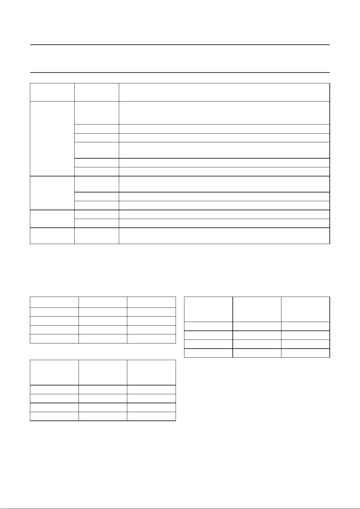
BUSY indicates the status of RECC, determined by a majority decision on the result of
TXABRT indicates that a RECC access attempt has been aborted without successful
TXIP 0 no transmission on RECC or RVC in progress
MSCC1,
MSCC0
LOGIC LEVEL DESCRIPTION
the last 3 consecutive Busy/Idle bits of the FOCC and is also routed to pin
BUSY/VSAT
0 channel idle
1 channel busy
indicates the result of the comparison of the incoming SAT and the stored SAT
Colour Code bits in the Voice Channel mode and is also routed to pin BUSY/VSAT
0 incoming SAT not equal to expected SAT
1 incoming SAT equal to expected SAT
message transmission
0 no access collision detected
1 transmission attempt aborted
1 data transmission by DPROC2 on RECC or RVC in progress
see Table 7 provides information about the current measured SAT colour code
Notes
1. Changing this register bit resets internally the receive and transmit logic circuitry.
2. Changing this register bit resets internally the receive logic circuitry.
Table 5 Set-up time of MVO signal
MR0 MR1 t
003
016
109
1112
Table 6 Expected SAT colour code
ESCC1 ESCC0
0 0 5970
0 1 6000
1 0 6030
1 1 no valid SAT
(ms)
MVO
SAT
FREQUENCY
(Hz)
Table 7 Measured SAT colour code
MSCC1 MSCC0
0 0 5970
0 1 6000
1 0 6030
1 1 no valid SAT
SAT
FREQUENCY
(Hz)
1997 Jan 28 12
Page 13
Philips Semiconductors Product specification
Data processor for cellular radio
(DPROC2)
Table 8 Conditions for transmission of received words to system controller
CHANGE IN CONTROL
FILLER WORD
DETECTED
REPEAT 2
REPEAT 2
OF WORD B
REPEAT 3
OF WORD A
DBCH DCFM
0 0 X X yes
010 0 no
010 1 yes
011 X yes
100 X yes
101 X no
110 0 no
110 1 yes
111 X no
handbook, full pagewidth
BIT
SYNC
WORD
SYNC
REPEAT 1
OF WORD A
BCH ERROR
BIT
REPEAT 1
OF WORD B
OF WORD A
UMA1002
TRANSMISSION OF CONTROL
FILLER WORD TO SYSTEM
CONTROLLER
REPEAT 3
OF WORD B
REPEAT 5
OF WORD B
BIT
SYNC
MVO
Fig.6 Timing of MVO output.
t
MVO
MLC095
1997 Jan 28 13
Page 14

Philips Semiconductors Product specification
Data processor for cellular radio
(DPROC2)
Digital circuit blocks
G
ENERAL
The majority of the digital circuitry within the DPROC2
device is identical for both AMPS and TACS. The
interconnections of the digital blocks discussed below are
shown in Fig.1.
D
ATA RECOVERY
The Data Recovery Block receives wideband Manchester
encoded data in sampled and sliced form from the
Comparator Block, on which it performs the following
functions:
• Clock recovery
• Manchester decoding
• Data regeneration.
The Clock Recovery Block extracts an 8 or 10 kHz (TACS
or AMPS) phase-locked clock signal from the Manchester
encoded data stream. This is implemented using a
digital-phase-locked-loop (PLL) which has an adjustable
‘bandwidth’ to provide both fast acquisition and low jitter.
Manchester decoding is performed by exclusive ORing the
recovered Manchester encoded data with the recovered
clock.
The NRZ data regeneration is performed by a digital
integrate and dump circuit. This consists of an up/down
counter that counts 1.2 MHz cycles during the data period.
The sense of the count is determined by the result of the
Manchester Decoder output. The number of counts is
sampled at the end of a data period. If this number
exceeds a threshold the data is latched as a logic 1
otherwise it is latched as a logic 0.
UMA1002
DETERMINATION
SAT
The SAT Determination Block indicates which, if any, of
the valid SAT tones is detected from the recovered SAT.
The AMPS and TACS specifications require that a
determination is made at least every 250 ms.
Determination involves counting the number of cycles of
the regenerated SAT in this time period. This count is then
compared to a set of four known counts which define the
boundaries between the SAT frequencies and
SAT-not-valid events. The result is then coded into the I2C
status registers MSCC0 and MSCC1.
SAT
REGENERATION
The SAT Regeneration Block generates a digital SAT
stream for transponding back to the base station.
The transponded SAT is phase-locked to the recovered
SAT by means of a second digital phase-locked-loop.
To minimize the total harmonic distortion of the output
signal the transponded SAT is then processed by a delta
modulator before being passed on to the Gated
Digital-to-Analog (D/A) converter.
OTTING DETECTOR
D
The Dotting Detector Block determines whether a data
inversion (dotting) pattern has been received on the
Forward Voice Channel. The detection of data inversion
indicates that the Clock Recovery Block has acquired bit
synchronization and that the narrow bandwidth mode on
the clock recovery phase-locked-loop is selected.
This signal is also used to indicate that a data burst is
expected and activates the audio mute RACTRL, after a
Word Synchronization Block has been received, for the
duration of the burst.
SAT
RECOVERY
The SAT Recovery Block receives a filtered and sliced
SAT signal which must be recovered before being routed
to the Determination and Regeneration Blocks.
The recovery is performed using a digital phase-locked
loop.
1997 Jan 28 14
Page 15

Philips Semiconductors Product specification
Data processor for cellular radio
(DPROC2)
WORD SYNCHRONIZATION DETECTOR
The Word Synchronization Block performs the following
functions:
• Frame Synchronization
• Reverse Control Channel status (B/I determination)
• Valid Serving System determination.
These functions are associated solely with the Forward
Control Channel and have no meaning on the Forward
Voice Channel.
Information in a data stream is identified by its position with
respect to a unique synchronization word.
This synchronization word is an 11-bit Barker code which
has a low probability of simulation in an error environment,
and can be easily detected. Data received is only
considered valid at times when DPROC2 has achieved
frame synchronization.
In this condition the block leaves its search mode and
enters its lock mode. This is indicated by bit WSYNC being
set HIGH. In order to achieve this two consecutive
synchronization words separated by 463 bits must be
detected. Once in lock mode, the synchronization word
detector is examined every 463 bits and only loses frame
synchronization after 5 consecutive unsuccessful
attempts at detecting the synchronization word have been
made. At this point bit WSYNC is cleared and the device is
returned to its search mode.
Information detailing the status of the Reverse Control
Channel is given by the Busy/Idle bits. These occur at
intervals of 11 bits within the frame, the first occurring
immediately following the synchronization word.
The status of the channel is determined by a majority
decision on the last three consecutive Busy/Idle bits.
FVC: After detection of 2 consecutive sync words the
circuit leaves its Search Mode and enters the Lock Mode.
The data word in between is considered as valid and
already stored for Majority Voting. Whenever a sync word
was found the incoming data stream is examined 88 bits
later for sync again. Whenever a valid sync word is
detected the following data word is given to the Majority
Voting block. After missing two consecutive sync words
the circuit goes back to the search mode (scanning for
sync every bit). If a sync word is then detected again, the
following data word is immediately accepted (and not only
after two correctly timed sync words). The detection
process of sync words is independent of the detection of
dotting. The audio mute via pin RACTRL is activated either
by receiving a sync word after detection of a dotting
sequence or by entering Lock Mode.
UMA1002
MAJORITY VOTING BLOCK
The Majority Voting Block performs the following functions:
• Identifying position and validity of frames in the received
data stream
• Extracting five repeats of each word from a valid frame
• Performing a bit-wise majority decision on the five
repeats of the data word.
The validity of the frames is determined by setting a
counter in operation which times out and resets the
circuitry after 920 or 463 bit periods from detecting valid
word synchronization. The time out period selected
depends on whether DPROC2 is monitoring the Forward
Voice or Control Channel respectively.
Up to five repeats of the message word are searched for
and extracted by DPROC2. On the Forward Voice
Channel the extraction of a data word for majority voting is
described in the Section “Word Synchronization Detector”.
DPROC2 enables two mechanisms for Majority Voting.
The first is based on 5 words and is described above.
The other mechanism is based on 3 consecutive identical
words and thus enabling switch-off of parts of the receiver
during reception of the remaining two words (see Table 5
and Fig.6).
E
RROR CORRECTION BLOCK
The Error Correction Block performs:
• Extraction of a valid message from the Majority-Voted
Word
• Computation of the S1 and S3 syndromes
• Correction of up to one error in the word
• Communication of received data to the System
Controller via the Received Data Serial Link.
Interpretation of parity of a received word is obtained from
knowledge of the syndromes of the word. The syndromes
are calculated using feedback shift registers with two
characteristic polynomials:
1+x+x6and1+x+x2+x4+x
Once the syndromes of a received word are known, it is
possible to determine if a correctable error is present.
DPROC2 only corrects up to one error although the code
used has a Hamming distance of five. The occurrence of
two or more errors is signalled by setting the BCH error
flag, which is communicated to the System Controller via
the Received Data Serial Link.
6
1997 Jan 28 15
Page 16

Philips Semiconductors Product specification
Data processor for cellular radio
(DPROC2)
RECEIVED DATA SERIAL LINK
The Received Data Serial Link transfers data and control
information from DPROC2 to the System Controller.
The data is transferred on RXLINE under control of a clock
signal RXCLK, generated by the System Controller.
The system controller is informed of the arrival of a
decoded data word in the DPROC2 output register by
RXLINE being driven LOW. If the system controller
chooses to ignore the received data or only partially clock
the data out, the DPROC2 will reset the receive buffer for
the next word after the period RWIN (see Fig.8).
Data format
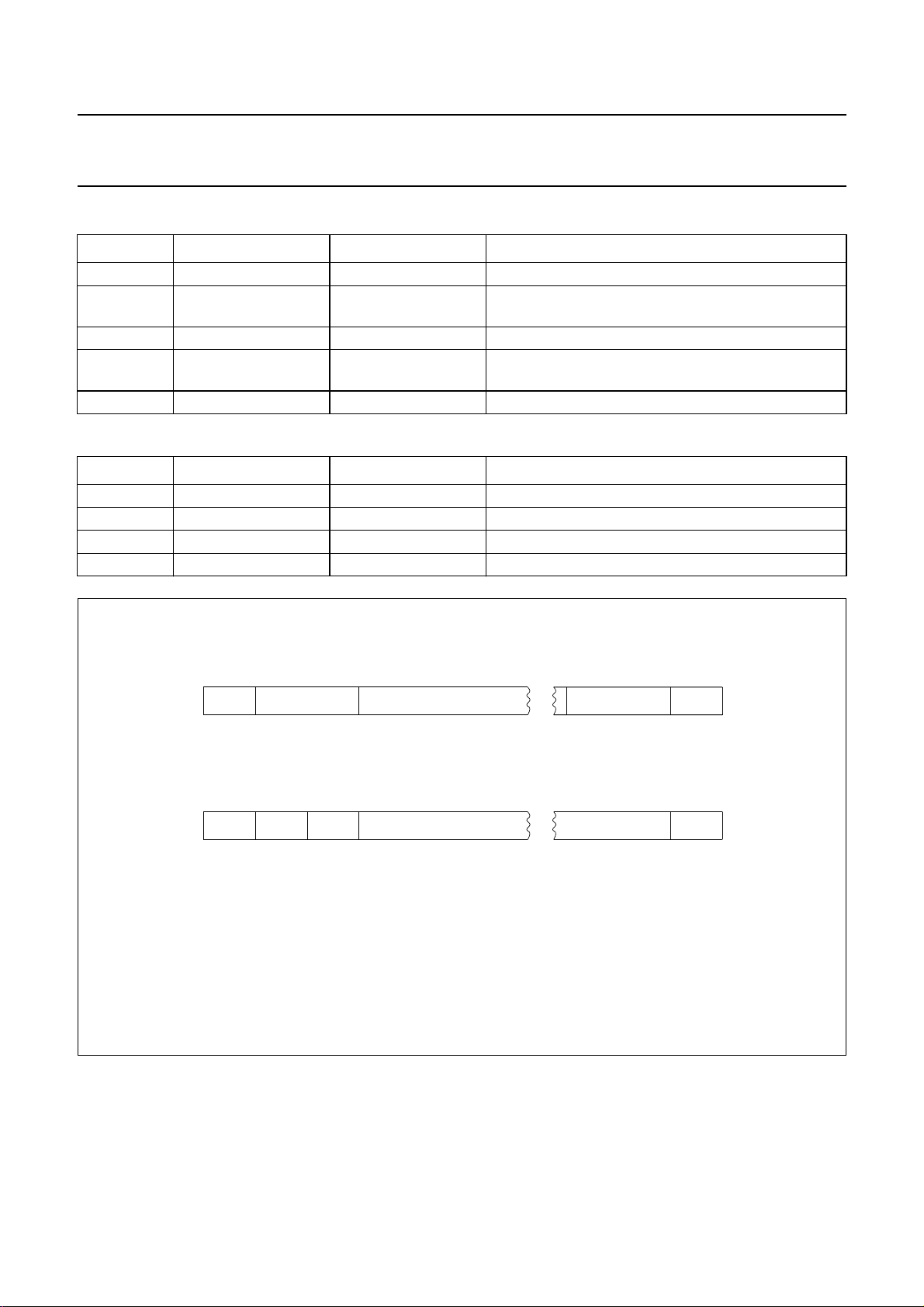
Each Received Data word consists of 4 bytes. The word
format is shown in Fig.7(a). The sense and function of the
fields is shown in Table 9.
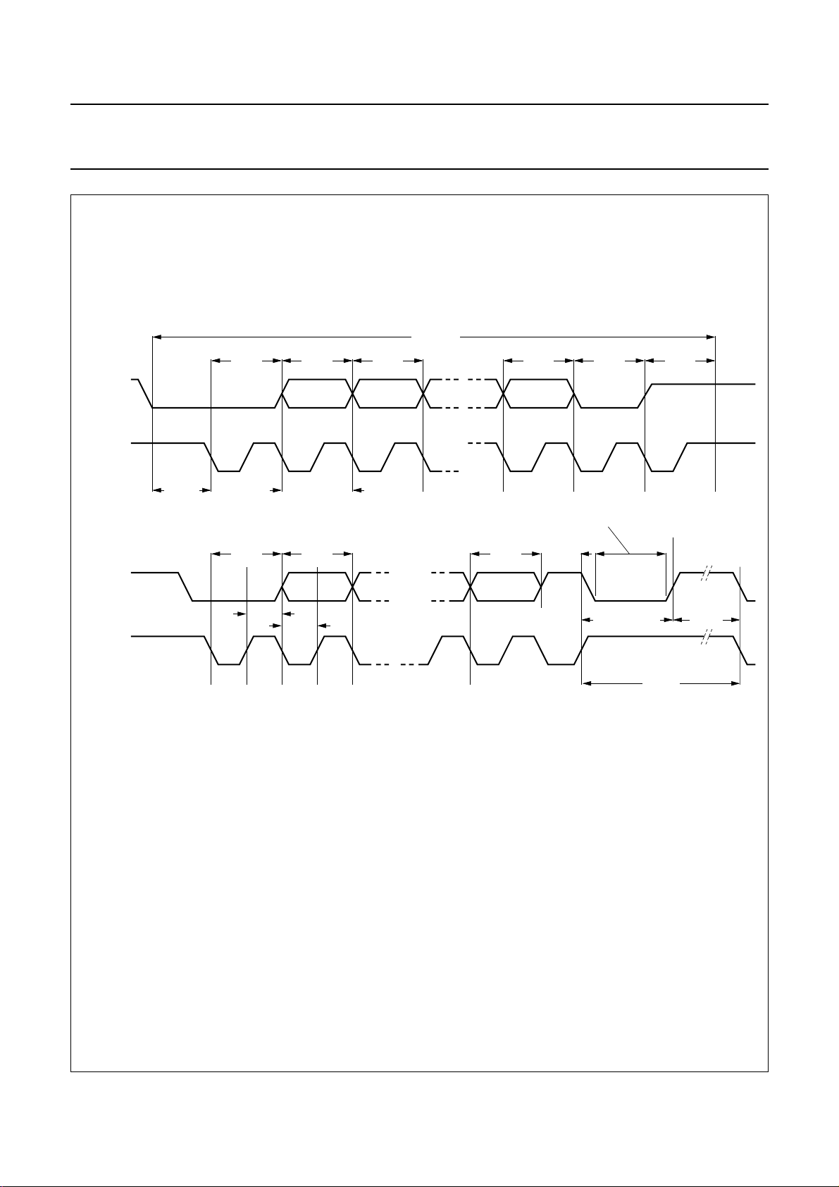
Link protocol
The Received Data protocol is described by the timing
diagram Fig.8(a) and has the following parameters:
• Maximum receive window (RWIN)
– Control Channel (TACS) = 47 ms; MAJ = 0
– Control Channel (TACS) = 30.5 ms; MAJ = 1
(in FOCC only)
– Control Channel (AMPS) = 37 ms; MAJ = 0
– Control Channel (AMPS) = 23.8 ms; MAJ = 1
(in FOCC only)
• Minimum clock period (t
• Minimum clock hold-off (t
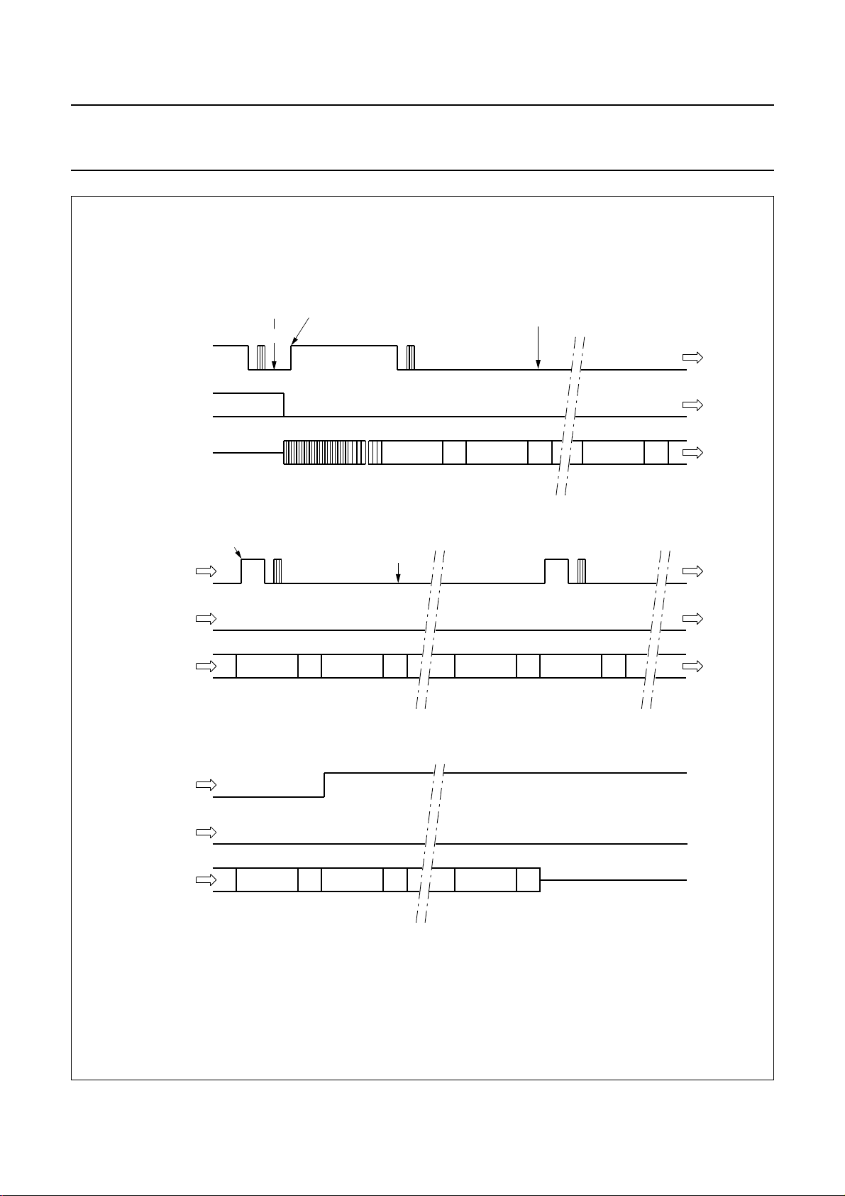
RANSMIT DATA SERIAL INTERFACE
T
The Transmit Data Serial Link performs reception of data
from the System Controller to DPROC2 over a dedicated
line TXLINE. The transfer of data is synchronous with a
clock signal TXCLK, generated by the System Controller.
CLKmin
WAIT
)=2µs
)=2µs.
UMA1002
Data format
Each Transmit Data word consists of 5 bytes. The word
format is shown in Fig.7(b). The sense and function of the
fields is shown in Table 10.
Link protocol
Messages are normally up to 5 words in length on the
Reverse Control Channel and up to 2 words in length on
the Reverse Voice Channel. However, DPROC2 will
transmit messages of any word length. These must be
transmitted on the data stream without interruption. To
avoid the need for large buffer areas, a flexible protocol is
used to allow DPROC2 to control the transfer of data
words. DPROC2 has an on-chip buffer which can hold one
complete word of a message. While new words are being
loaded into DPROC2, within the time period Buffer clear to
end of TWIN, DPROC2 will maintain uninterrupted data
transmission. The System Controller can abort the
transmission of a message at any point activating the
I2C-bus signal TXRST. This signal causes the interface to
return to its power-up state and resets TXIP and TXABRT
(see Table 4). On completion of these tasks TXRST will
return to its inactive state. The Transmit Data Protocol is
described by the timing diagram shown in Fig.8(b) and has
the following parameters:
• Maximum transmit window (TWIN)
– voice channel (TACS) = 60 ms
– voice channel (AMPS) = 48 ms
– control channel (TACS) = 29 ms
– control channel (AMPS) = 23 ms
• Minimum clock period (t
• Minimum wait period (t
Note that TXRST will clear the transmit buffer.
WAIT
CLKmin
)=2µs.
)=2µs
1997 Jan 28 16
Page 17
Philips Semiconductors Product specification
Data processor for cellular radio
UMA1002
(DPROC2)
Table 9 Received data word
BIT TITLE SENSE FUNCTION
31 start LOW identifies start of word
30 BCH error active HIGH indicates that an uncorrected BCH error is associated
with the word
29 to 2 received data binary data received data word
1 RXLINE error active HIGH indicates that a transmission error has occurred on
the microprocessor to DPROC2 serial link
0 stop HIGH identifies end of the word
Table 10 Transmit data word
BIT TITLE SENSE FUNCTION
39 start LOW identifies start of word
38 and 37 DCC binary data digital colour code (see Table 11)
36 to 1 transmit data binary data transmit data word
0 stop HIGH identifies end of the word
handbook, full pagewidth
(a) Received data word.
(b) Transmit data word.
MSB
START BCH ERROR
MSB
START DCC 1 DCC 0
LSB
RECEIVED WORD (28 bits)
(a)
TRANSMIT WORD (36 bits)
Bit 36Bit 38Bit 39 Bit 37 Bit 1 Bit 0
(b)
CHECK BIT (= 0) STOP
Bit 1 Bit 0Bit 2Bit 29Bit 30Bit 31
LSB
STOP
Fig.7 Data word formats.
MBC768
1997 Jan 28 17
Page 18
Philips Semiconductors Product specification
Data processor for cellular radio
(DPROC2)
handbook, full pagewidth
bit 31 bit 30 bit 29 bit 2 bit 1 bit 0
RXLINE
RXCLK
t
WAIT
bit 39 bit 38
t
CLK (min)
RWIN
(a)
DPROC holds TXLINE LOW
during encoder stage
bit 1 bit 0
(2)
UMA1002
buffer clear
TXLINE
t
TXCLK
h
t
su
buffer busy
(1)
TWIN
t
WAIT
MBC769
(b)
(1) The buffer time depends on whether the first or subsequent words are being loaded.
(2) The system controller should monitor the TXLINE during bit 0, if the status of TXLINE does not change from a HIGH-to-LOW on the rising edge of
TXCLK, then a framing error has occurred. This can be caused by glitches on the clock line or if an arbitration error occurred while the DPROC2
transmit register was being loaded. The system controller should recover the situation by holding TXLINE HIGH and supplying clocks on TXCLK
until TXLINE goes LOW. Then the situation should be treated as a normal channel arbitration failure as described in Section “Reverse Control
Channel Access Arbitration” - “Abort procedure (see Fig.10)”.
(a) DPROC2 to microcontroller link; receive data timing.
(b) Microcontroller to DPROC2 link; transmit data timing.
Where:
> 100 ns
t
h
> 500 ns.
t
su
Fig.8 Data timing diagrams.
1997 Jan 28 18
Page 19

Philips Semiconductors Product specification
Data processor for cellular radio
(DPROC2)
BCH AND MANCHESTER ENCODING BLOCK
The functions performed by this circuit block include:
• Reception of data from the System Controller
• Parity generation
• Message construction
• Manchester encoding.
Each 36-bit Information Word sent on the Reverse Voice
and Control Channels is coded into a 48-bit code word.
The code word consists of the 36-bit word followed by
12 parity bits. These parity bits are formed by clocking the
information word into a 12-bit feedback shift register with
characteristic polynomial:
3+x4+x5+x8+x10+x12
1+x
The BCH Encoder Block constructs the Reverse Voice
and Control Channel data streams from the information it
receives from the System Controller.
The streams are formed out of the four possible field types:
• Dotting (data inversions)
• 11-bit Synchronization Word
• Digital Colour Code (see Table 11)
• 48-bit code word.
The 2 bits of DCC received from the System Controller are
coded into a 7-bit word as shown in Table 11.
The data sense for Manchester Encoding has a NRZ
logic 1 encoded as a 0-to-1 transition and a NRZ logic 0
encoded as a 1-to-0 transition.
UMA1002
R
EVERSE CONTROL CHANNEL ACCESS ARBITRATION
The AMPS and TACS specifications require a method of
arbitration on the Reverse Control Channel to prevent two
mobiles from transmitting on the same channel at the
same time.
This function is performed by DPROC2 monitoring the
Busy/Idle stream sent on the Forward Control Channel.
The AMPS and TACS specifications state that once the
mobile has commenced transmitting on the Reverse
Control Channel it must monitor the Busy/Idle stream.
If this stream becomes active outside a predetermined
‘window’, measured from the start of the transmission of
the message, the mobile must terminate its transmission
and disable the transmitter immediately.
In the Cellular Radio chip-set there are two levels of control
of the RF transmitter; the first is absolute control by the
System Controller, the second is conditional by other
devices in the set. In DPROC2 the conditional control of
the transmitter is performed via the output TXCTRL.
This line is effectively wired ORed together, using
open-drain outputs, with other devices which may wish to
control the transmitter. When these devices do not wish to
disable the transmitter their output is in a HIGH impedance
state.
An exception to this procedure occurs when the Serving
System instructs the mobile not to monitor the Busy/Idle
bits. In this event the arbitration logic can be disabled by
clearing I
The flow of events during a Control Channel Access
attempt is as follows:
2
C-bus register bit ABREN.
Initial state
• Transmitter disabled
• DPROC2 transmit circuitry in power-up state
• TXCTRL line HIGH.
Table 11 Digital colour code; 7-bit word
DCC1 DCC0 CODED DCC
000000000
010011111
101100011
111111100
1997 Jan 28 19
Page 20

Philips Semiconductors Product specification
Data processor for cellular radio
(DPROC2)
Access attempt procedure
1. System Controller decides to send message
2. System Controller drives TXCTRL LOW directly.
3. System Controller switches transmitter power-on and
waits for power-up for the transmitter module (RF
transmitter is still disabled by TXCTRL).
4. System Controller sets TXRST via I2C-bus to
DPROC2.
5. System Controller sets ABREN via I2C (if required)
allowing DPROC2 to control the transmitter.
6. System Controller determines status of Reverse
Control Channel by monitoring the Busy/Idle bit.
If busy, waits a random time then tries again.
7. System Controller releases TXCTRL allowing it to be
pulled HIGH enabling the transmitter output.
8. System Controller transfers the first word of the
message to DPROC2 via serial link
(1)
9. DPROC2 sets I2C-bus signal TXIP and starts sending
message while monitoring Busy/Idle status.
10. If channel becomes busy before 56 bits and ABREN is
set then perform Abort Procedure.
11. If channel remains idle after 104 bits and ABREN is set
then perform Abort Procedure.
12. System controller loads the subsequent words of the
message into DPROC2 when the buffer becomes
clear as shown in Fig.8(b).
13. On completion of entire message DPROC2 clears
TXIP and 25 ms later the System Controller disables
transmitter via I2C-bus.
14. System Controller finally sends TXRST to prepare
DPROC2 for next transmission.
(1)
.
.
UMA1002
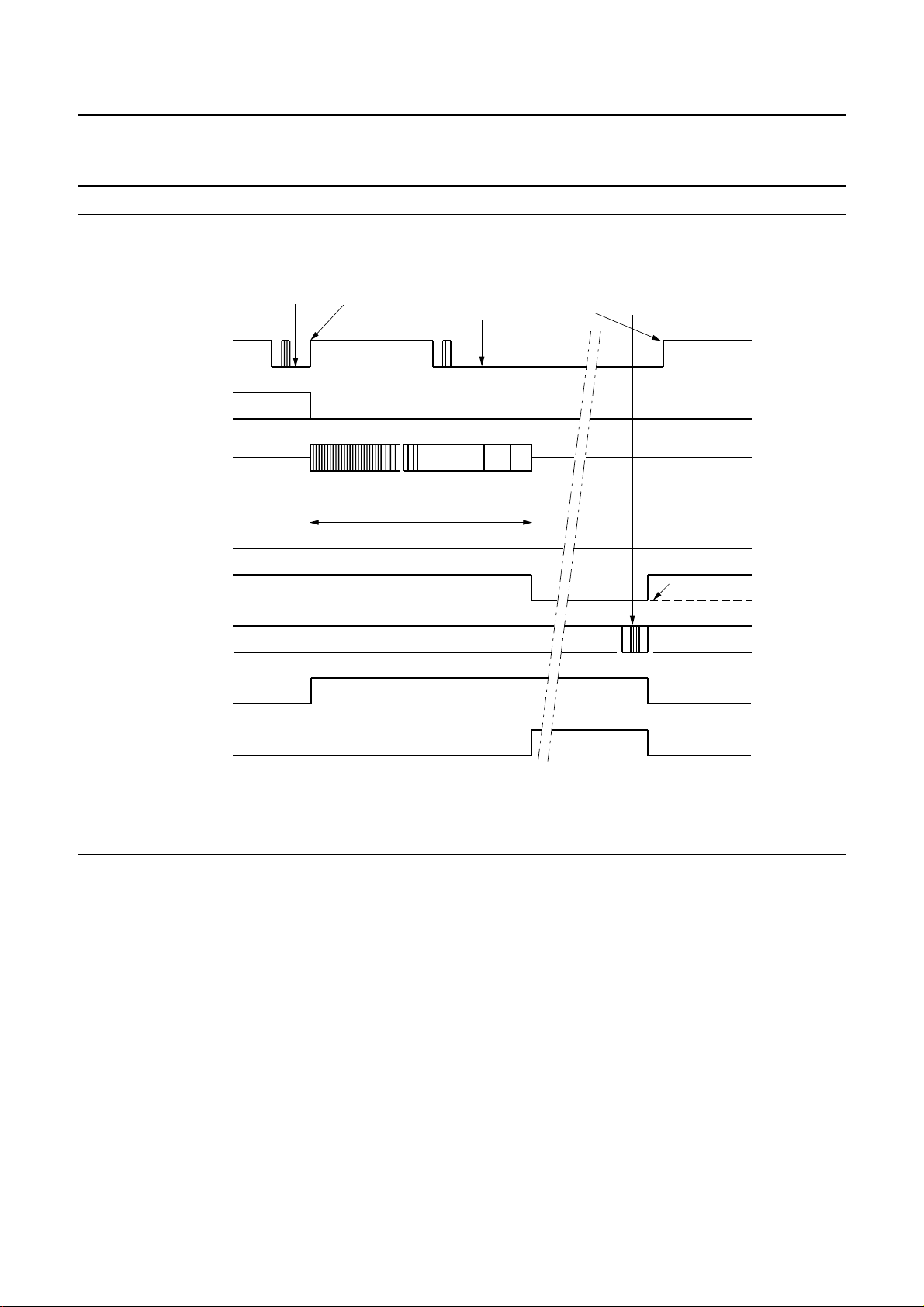
Abort procedure (see Fig.10)
1. DPROC2 immediately disables transmitter output by
driving TXCTRL LOW.
2. DPROC2 sets TXABRT.
3. System Controller detects failure by monitoring
TXCTRL and TXABRT.
4. System Controller disables transmitter via RF power
amplifier.
5. System Controller sends TXRST to prepare DPROC2
for next transmission.
S
IGNAL TONE GENERATION (ST)
The 8 or 10 kHz (TACS or AMPS) tone generated from the
Manchester Encoding Block is used as the Signalling Tone
stream.
(1) At stage 1 the system controller may choose to preload
DPROC2 with the first word of the message and hold it from
transmission until stage 7 using the TXHOLD line. This gives
a lower time overhead between detecting an IDLE channel
and commencing the transmission. To use this feature
TXHOLD must be driven HIGH before the last bit of data has
been transferred into DPROC2. Figure 9 illustrates the
DPROC2 data transmission timing.
1997 Jan 28 20
Page 21
Philips Semiconductors Product specification
Data processor for cellular radio
(DPROC2)
handbook, full pagewidth
TXHOLD
DPROC2 data
TXLINE
continued
TXLINE
DPROC2
holds LOW
TXLINE
word 1 word 2
DPROC2
releases
TXLINE
word 3
DPROC2
releases
TXLINE
dotting W.S. DCC word 1
30 11 7
repeat1
36
DPROC2
holds LOW
TXLINE
Parity
12
word 1
repeat 2
36
DPROC
holds LOW
TXLINE
Parity
12
word 4
word 1
repeat 5
36
UMA1002
Parity
12
TXHOLD
continued
DPROC2 data
continued
TXLINE
continued
TXHOLD
continued
DPROC2 data
continued
Parity
12
Parity
12
word 2
repeat 1
36
word n
repeat 1
36
Parity
12
Parity
12
word 2
repeat 2
36
word n
repeat 2
36
Parity
12
Parity
12
word 2
repeat 5
36
word n
repeat 5
36
Parity
12
Parity
12
word 3
repeat 1
36
Parity
12
MEA173
Fig.9 DPROC2 data transmission timing/microcontroller interface.
1997 Jan 28 21
Page 22
Philips Semiconductors Product specification
Data processor for cellular radio
(DPROC2)
handbook, full pagewidth
TXLINE
TXHOLD
DPROC2 data
BUSY
TXCTRL
DPROC2
holds LOW
TXLINE
word 1 word 2
DPROC2
releases
TXLINE
dotting W.S. DCC word 1
30 11 7
104 bits
DPROC2
holds LOW
repeat1
36
TXLINE
Parity
arbitration failure
Busy/Idle stream
remains Idle
after 104 bits
word 1
repeat 2
12
truncated
2
C-bus
I
send
TXRST
to DPROC2
UMA1002
DPROC2
ready for
new transmisson
has to be controlled
by system controller
I2C-bus
TXIP
TXABRT
MEA172
Fig.10 DPROC data transmission timing/microcontroller interface during arbitration failure.
1997 Jan 28 22
Page 23

Philips Semiconductors Product specification
Data processor for cellular radio
(DPROC2)
Analog circuit blocks
G
ENERAL
The analog signal processing functions on DPROC2 are
implemented using switched-capacitor techniques.
The main filtering functions are operated at 300 kHz, and
these circuits are ‘interfaced’ to the continuous time and
sampled digital domains by RC active filters, passive
interpolators and comparators.
The RC sections, the Anti-Alias Filter and the Clock Filter,
are non-critical and are designed to tolerate process
spreads. The critical filtering in the SAT Filter and the
Output Filter, is performed by 300 kHz switched-capacitor
circuitry. The Passive Interpolator increases the sampling
rate from 300 kHz to 1.2 MHz. The sampled analog
signals from the Passive Interpolator is converted to a
sampled 2-state digital signal by a Comparator. The Gated
D/A converter blocks and Analog Summer block together
perform resynchronization and sub-sampling of the
digitally generated DPROC2 output signals, and
conversion to the sampled analog domain.
These analog sections of the device are shown in Fig.1.
B
IAS GENERATOR
The Bias Generator generates the analog ground
reference voltage (AGND) used internally within the
DPROC2 device. To minimize noise AGND must be
externally decoupled to V
contains a current reference to generate all bias currents
for the analog circuits.
A
NTI-ALIASING FILTER
The Anti-Aliasing Filter is placed before the SAT filter block
to prevent any unwanted signals or high-frequency noise
present on the DEMODD pin being aliased into the
pass-band by the sampling action of the
switched-capacitor filter. To achieve this the Anti-Aliasing
Filter is a time-continuous RC-active low-pass filter.
SAT I
NPUT FILTER
The SAT Input Filter is a switched-capacitor filter which
provides band-pass filtering of the SAT signals from the
DEMODD pin to improve the SAT signal-to-noise ratio
prior to recovery and transponding.
ASSIVE INTERPOLATOR
P
The function of the Passive Interpolator is to increase the
sampling rate at the output of the SAT filter. This reduces
the coarseness of the zero-crossing information which
as shown in Fig.12. It also
SSA
UMA1002
would otherwise cause unacceptable isochronous
distortion in the recovered signal.
OMPARATORS
C
The Comparators form the analog-to-digital interface for
the received data and SAT signals from the DEMODD pin.
These comparators act as limiting amplifiers which convert
the filtered sampled analog signals into 2-state sampled
digital signals containing only the zero-crossing
information from the analog signal. To prevent unwanted
signals being processed by the digital circuitry both
comparators have a hysteresis implemented
ATED D/A CONVERTERS AND ANALOG SUMMER
G
The Gated D/A converters and Analog Summer form the
interface between the digital and analog circuitry on the
transmit path of DPROC2. It is at this point that the three
sampled digital signals, containing SAT, ST and encoded
digital data, are combined to form a composite signal.
The data streams are enabled by the I2C signals STEN,
SATEN and the internal signal DATAEN respectively
(DATAEN disables SAT and ST when data is being
transmitted). The digital-to-analog conversion and
sub-sampling operation is performed by the Gated D/A
converters and Analog Summer.
The typical relative signal weights applied in the summer
(with respect to the data path) are shown in Table 12.
Table 12 Typical relative signal weight
SIGNAL
ST or DATA 1.0
SAT 0.25
OUTPUT FILTER
The Output Filter is a switched-capacitor filter which
performs band-limiting of the DPROC2 output signals in
accordance with the AMPS and TACS specifications.
The required below band roll-off is achieved via external
AC-coupling from the DATA pin.
C
LOCK FILTER
The Clock Noise Filter is a non-critical continuous time
RC-active low-pass filter used to remove any switching
transient residues from the output signal. It contains an
output driver stage to provide a low output impedance and
sufficient driving capability for the pin DATA.
RELATIVE OUTPUT LEVEL
AMPS AND TACS
1997 Jan 28 23
Page 24
1997 Jan 28 24
b
ook, full pagewidth
APPLICATION INFORMATION
(DPROC2)
Philips Semiconductors Product specification
Data processor for cellular radio
NE620 OR DISCRETE SOLUTION
VCO
UMA1015
PA
BGY118A/B
BGY115A/B
5 V
VCO
SECOND IF
TCXO
9.6 MHz
3-wire control bus
POWER CONTROL
NE606
RSSI
DEMOD
QUAD
TANK
MOD
POWER CONTROL
UMA1002 P83CL580
DATA
1.2 MHz
NE5753
NE5752 TDA7050
1.2 MHz
2
I C bus
PSD312L
keyboard
scan bus
chip-on-glass
LCD
5 V DC-DC 3 V
Fig.11 Cellular radio system schematic for AMPS/TACS.
MBD830
UMA1002
Page 25
1997 Jan 28 25
a
RECEIVER
SUBSYSTEM
1.2 MHz
OUTPUT
demodulated data/audio
270 pF
1.2 MHz
2.2
µF
10 nF
100 kΩ
100
n.c.
nF
10 µF
100
RECDATA
TST
DEMODD
AGND
V
SSA
V
SSD
INVTX
INVRX
CLKOUT
CLKIN
ndbook, full pagewidth
V
DDD
3 V)(
nF
SDA SCL
28 24 25
10
9
3
2
DATA PROCESSOR
1
14
21
7
13
12
420115
DATA TXCTRL TACTRL RACTRL
UMA1002T
19
8
27
15
18
17
6
16
22
23
BUSY/VSAT
RXLINE
RXCLK
TXLINE
TXCLK
TXHOLD
RESET
n.c.
TSCAN
(+3 V)
A0
I2C interface
MICROCONTROLLER
(PCB80C552)
GENERAL PURPOSE
I/O ports
V
DDD
(+3 V)
Philips Semiconductors Product specification
Data processor for cellular radio
(DPROC2)
TRANSMITTER
SUBSYSTEM
TXDIS
modulation
line
CLKIN
MODOUT
DEMOD
AGND
AUDIO PROCESSOR
10 nF
DATA
TX
MUTE
VOX
+
RX
MUTE
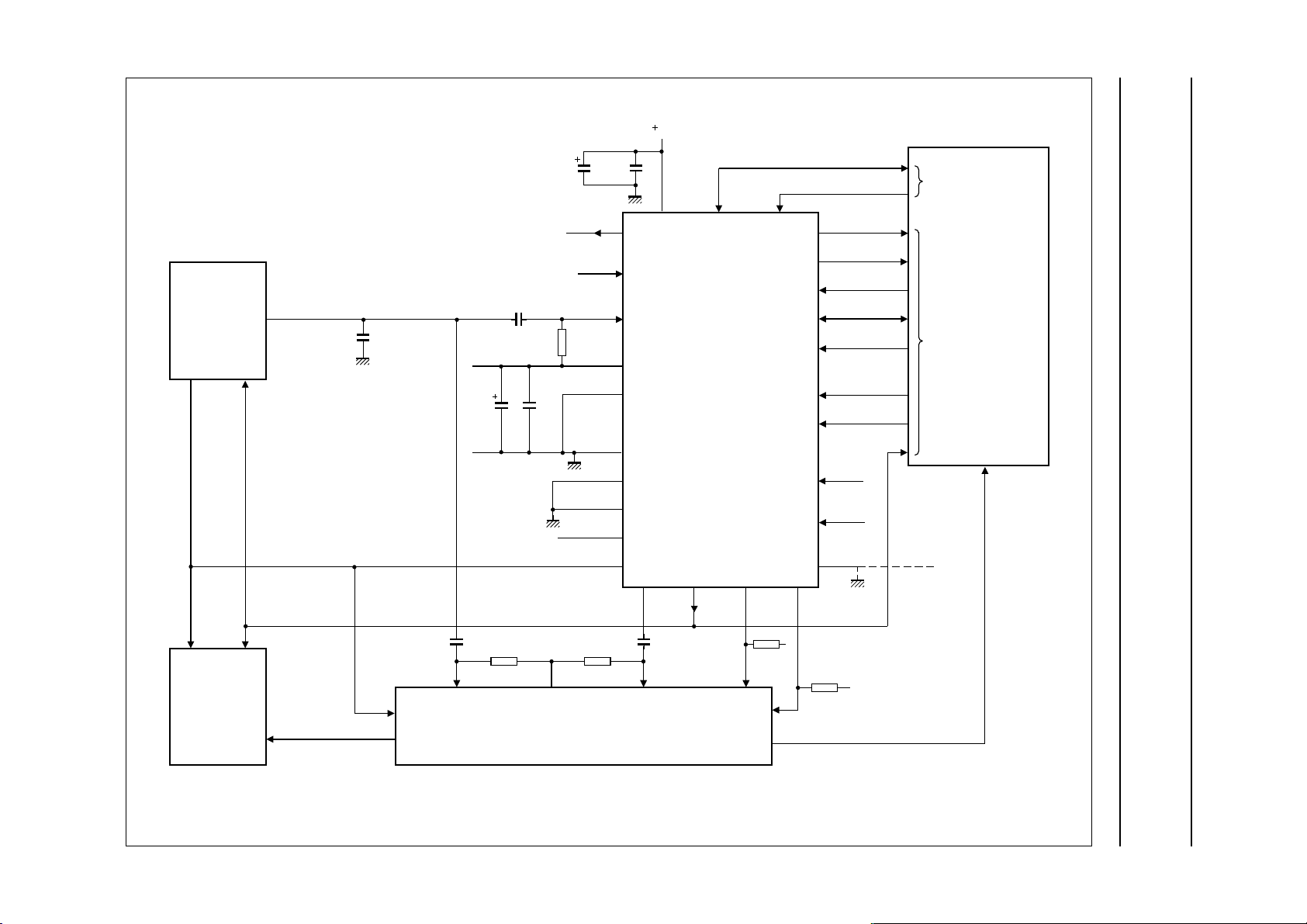
Fig.12 DPROC2 baseband application circuit (SO28, SOT136-1).
+
UMA1002
MBD833
Page 26
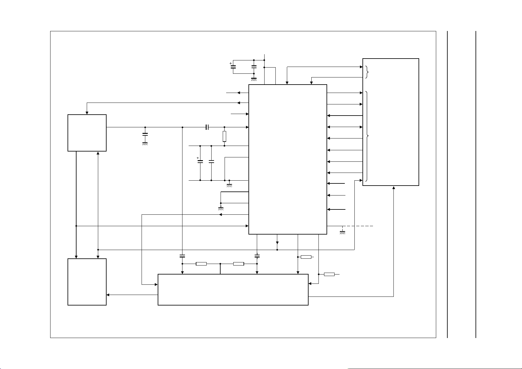
1997 Jan 28 26
RECEIVER
SUBSYSTEM
9.6 MHz
OUTPUT
demodulated data/audio
270 pF
9.6 MHz
1.2 MHz
2.2
µF
10 nF
100 kΩ
10 µF
100
nF
100
RECDATA
MVO
TST
DEMODD
AGND
V
SSA
V
SSD
INVTX
INVRX
CLKOUT
CLKIN
V
DDD
(+3 V)
V
DDA
nF
8
3
7
31
30
29
12
21
4
11
10
(+3 V)
SDA SCL
27 2428 25
DATA PROCESSOR
UMA1002H
32 19 9 1
DATA TXCTRL TACTRL RACTRL
17
26
13
16
15
14,18
20
22
23
BUSY/VSAT
RXLINE
5
RXCLK
TXLINE
TXCLK
TXHOLD
RESET
2
JTACS
6
n.c.
CLKSEL
(+3 V)
TSCAN
(+3 V)
A0
I2C interface
MICROCONTROLLER
(PCB80C552)
GENERAL PURPOSE
I/O ports
V
DDD
(+3 V)
Philips Semiconductors Product specification
Data processor for cellular radio
(DPROC2)
TRANSMITTER
SUBSYSTEM
TXDIS
modulation
line
10 nF
DEMOD
CLKIN
MODOUT
AGND
AUDIO PROCESSOR
Fig.13 DPROC2 baseband application circuit (LQFP32, SOT358-1).
DATA
handbook, full pagewidth
TX
MUTE
VOX
+
RX
MUTE
+
UMA1002
MGC630
Page 27
1997 Jan 28 27
a
ndbook, full pagewidth
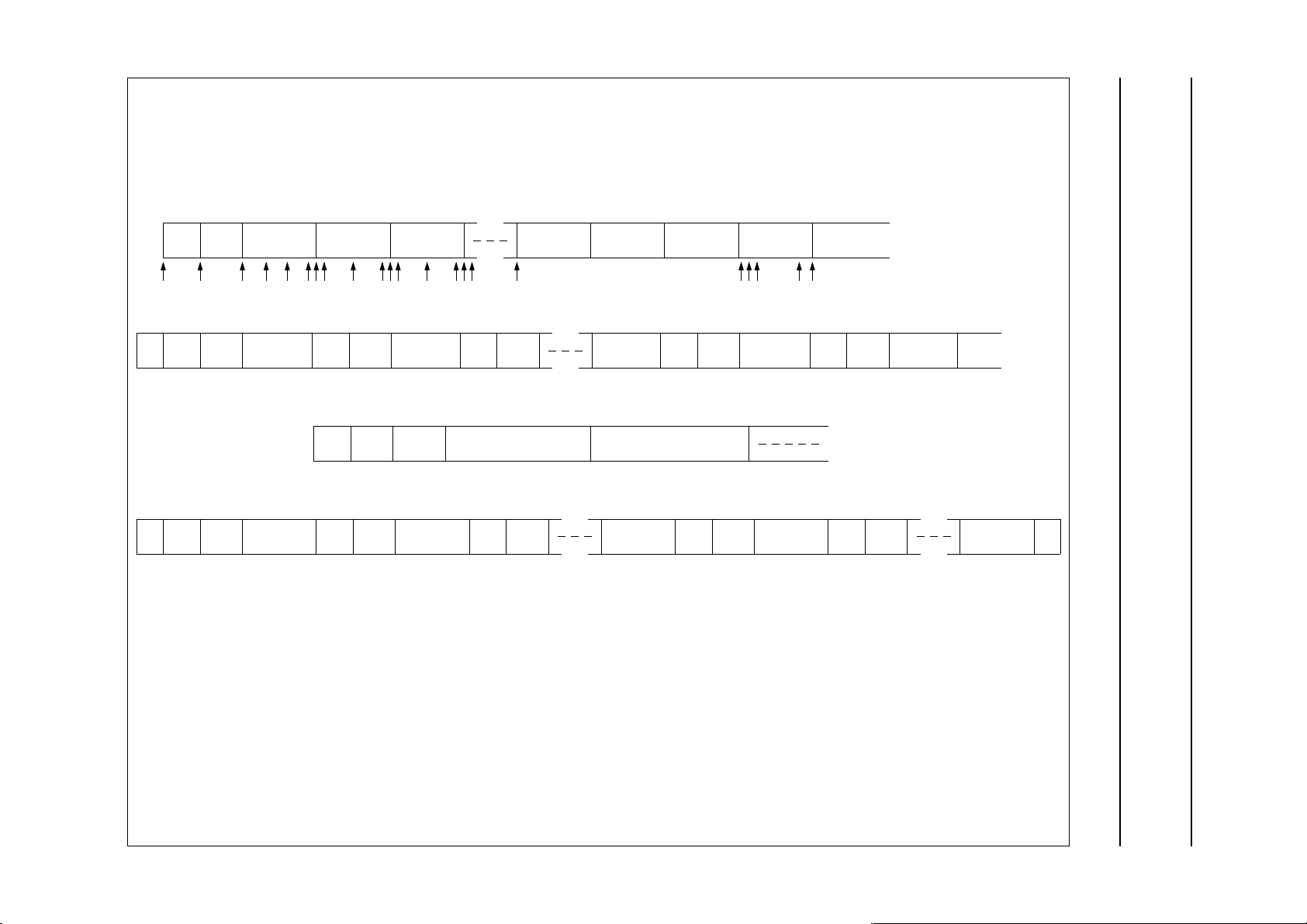
SIGNALLING FORMATS
(DPROC2)
Philips Semiconductors Product specification
Data processor for cellular radio
10 11
BIT
WORD
SYNC
SYNC
Busy/Idle
Bit
11 40 37
101
BIT
WORD
SYNC
SYNC
11 48
101
BIT
WORD
SYNC
SYNC
40
REPEAT 1
OF WORD A
REPEAT 1
OF WORD
REPEAT 1
OF WORD 1
40
REPEAT 1
OF WORD B
40
REPEAT 2
OF WORD A
40
REPEAT 4
OF WORD A
40 40 40
REPEAT 4
OF WORD B
(a)
11 37
BIT
WORD
SYNC
SYNC
REPEAT 2
OF WORD
BIT
SYNC
1140
WORD
SYNC
REPEAT 9
OF WORD
(b)
30 11 7 240 240
BIT
SYNC
WORD
SYNC
CODED
DCC
FIRST WORD REPEATED
5 TIMES
SECOND WORD REPEATED
5 TIMES
(c)
37
BIT
SYNC
11 48
WORD
SYNC
REPEAT 2
OF WORD 1
37
BIT
SYNC
11
WORD
SYNC
(d)
48
REPEAT 5
OF WORD 1
REPEAT 5
OF WORD A
37
1140
BIT
WORD
SYNC
SYNC
37
BIT
SYNC
REPEAT 5
OF WORD B
40 37
REPEAT 10
OF WORD
11 48
WORD
SYNC
REPEAT 1
OF WORD 2
10
BIT
SYNC
BIT
SYNC
11 40
WORD
SYNC
37
BIT
SYNC
11
WORD
SYNC
REPEAT 11
OF WORD
48
REPEAT 5
OF WORD 2
MBC770
(a) FOCC (Forward Control Channel).
(b) FVC (Forward Voice Channel).
(c) RECC (Reverse Control Channel).
(d) RVC (Reverse Voice Channel).
UMA1002
Fig.14 Signalling formats.
Page 28
Philips Semiconductors Product specification
Data processor for cellular radio
UMA1002
(DPROC2)
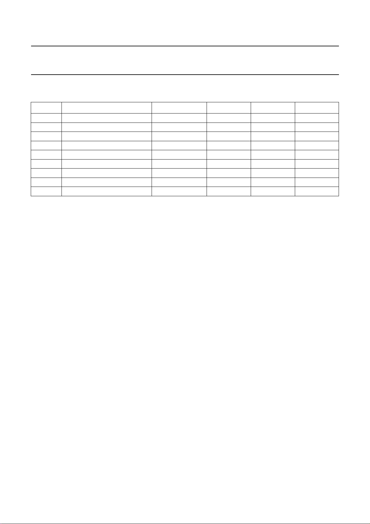
LIMITING VALUES
In accordance with Absolute Maximum Rating System (IEC 134).
SYMBOL PARAMETER CONDITIONS MIN. MAX. UNIT
V
DD
I
DD
I
I
I
O
V
I
P
tot
P
o
T
amb
T
stg
supply voltage −0.5 +6.5 V
supply current − 50 mA
DC input current (any input) −±10 mA
DC output current (any output) −±10 mA
input voltages (all inputs) V
DD(max)
=6V −0.5 VDD+ 0.5 V
total power dissipation − 300 mW
power dissipation per output − 10 mW
operating ambient temperature −30 +70 °C
storage temperature −65 +150 °C
1997 Jan 28 28
Page 29
Philips Semiconductors Product specification
Data processor for cellular radio
UMA1002
(DPROC2)
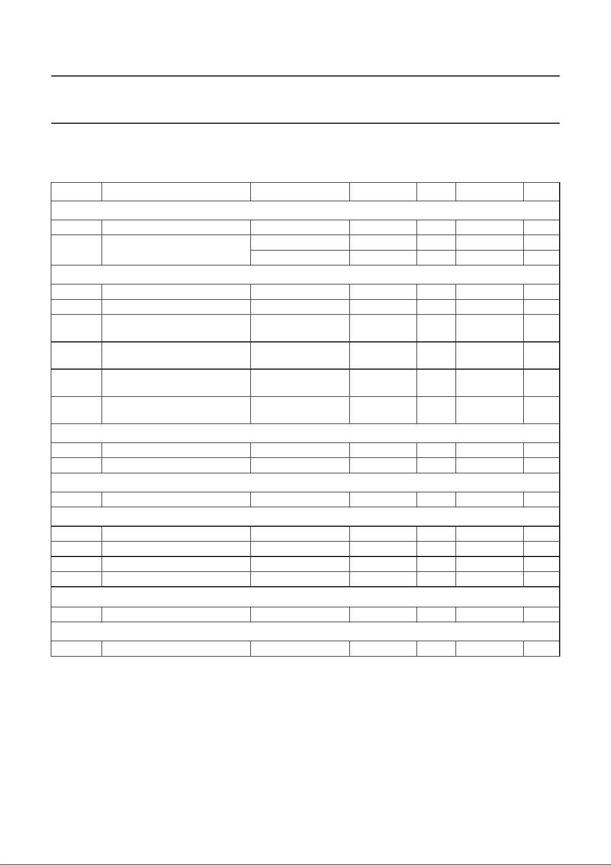
DC CHARACTERISTICS
V
= 3 V (V
DD
unless otherwise specified.
SYMBOL PARAMETER CONDITIONS MIN. TYP. MAX. UNIT
Supply
V
DD
I
DD
Digital inputs: INVRX, INVTX, CLKSEL, TXHOLD, TXCLK, A0, RESET, RXCLK, TST, TSCAN, CLKIN and JTACS
V
IL
V
IH
I
LI
R
pdCLKSEL
R
pdJTACS
R
pdTST
DDA
and V
externally connected); T
DDD
= −30 to +70 °C; f
amb
= 1.2 MHz (if CLKSEL = logic 0);
CLKIN
supply voltage 2.7 3.0 5.5 V
operating supply current at pins
V
and V
DDD
DDA
LOW level input voltage −0.3 − 0.3V
HIGH level input voltage 0.7V
LOW/HIGH level input leakage
current
CLKSEL internal pull-down
in FVC − 1.3 1.8 mA
in FOCC − 0.4 − mA
DD
− VDD+ 0.3 V
pins without
DD
−−1µA
pull-down
− 200 − kΩ
resistance
JTACS internal pull-down
− 200 − kΩ
resistance
TST internal pull-down
− 200 − kΩ
resistance
V
Digital push-pull outputs: RXLINE, BUSY/VSAT, RECDATA, MVO and CLKOUT
V
OL
V
OH
LOW level output voltage I
HIGH level output voltage I
=1mA −−0.4 V
sink
= −1mA VDD− 0.4 −− V
source
Open-drain n-channel outputs: TXCTRL, TACTRL and RACTRL
V
OL
LOW level output voltage I
=2mA −−0.4 V
sink
Open-drain n-channel input/output: TXLINE
V
OL
V
IL
V
IH
R
puTXLINE
2
C-bus pins: SCL and SDA
I
t
data
LOW level output voltage I
=2mA −−0.4 V
sink
LOW level input voltage −0.3 − 0.3V
HIGH level input voltage 0.7V
DD
internal pull-up resistance − 100 − kΩ
data conversion rate −−100 kbits/s
Analog reference pin: AGND
V
AGND
DC voltage level for VDD= 2.7 to 5.5 V − 0.5VDD− V
DD
− VDD+ 0.3 V
V
1997 Jan 28 29
Page 30
Philips Semiconductors Product specification
Data processor for cellular radio
UMA1002
(DPROC2)
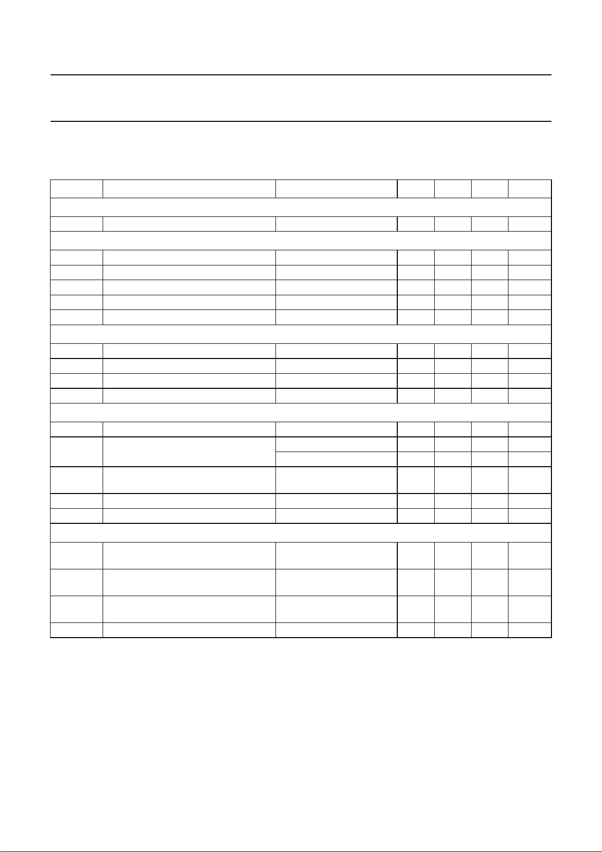
AC CHARACTERISTICS
V
= 3 V (V
DD
unless otherwise specified.
SYMBOL PARAMETER CONDITIONS MIN. TYP. MAX. UNIT
Data rate of data transfer link: RXCLK, RXLINE, TXCLK, TXLINE
t
data
Clock input: CLKIN (CLKSEL = logic 0)
C
i
T
CLKIN
t
CLKINH
t
r
t
f
Clock input: CLKIN (CLKSEL = logic 1)
T
CLKIN
t
CLKINH
t
r
t
f
Analog output: DATA
V
DATA
V
o(p-p)
THD total harmonic distortion for
R
L
C
L
Analog input: DEMODD
V
DEMODD
V
i(p-p)
V
i(p-p)
Z
i
DDA
and V
externally connected); T
DDD
= −30 to +70 °C; f
amb
= 1.2 MHz (if CLKSEL = logic 0);
CLKIN
data conversion rate −−500 kbit/s
input capacitance − 5 − pF
clock input period time 833.25 833.33 833.42 ns
clock input HIGH time 40 50 60 %T
clock input rise time − 50 − ns
clock input fall time − 50 − ns
clock input period time − 104.17 − ns
clock input HIGH time 40 50 60 %T
clock input rise time − 5 − ns
clock input fall time − 5 − ns
DC output voltage level − V
output voltage level for signalling tone
(peak-to-peak value)
VDD= 3 V; note 1 1.14 1.2 1.26 V
V
= 5 V; note 1 1.9 2.0 2.1 V
DD
AGND
− V
−−10 %
Supervisory Audio Tone (SAT)
allowed load resistance to AC ground 10 −−kΩ
allowed load capacitance to AC ground −−100 pF
DC input voltage level 100 kΩ resistor external to
− V
AGND
− V
AGND
data input voltage level
input via a 10 nF capacitor 200 250 600 mV
(peak-to-peak value)
SAT input voltage level
50 −−mV
(peak-to-peak value)
input impedance 1 −−MΩ
CLKIN
CLKIN
Note
1. Plus supply voltage variation (∆V
), RL=10kΩ.
DD
1997 Jan 28 30
Page 31
Philips Semiconductors Product specification
Data processor for cellular radio
(DPROC2)
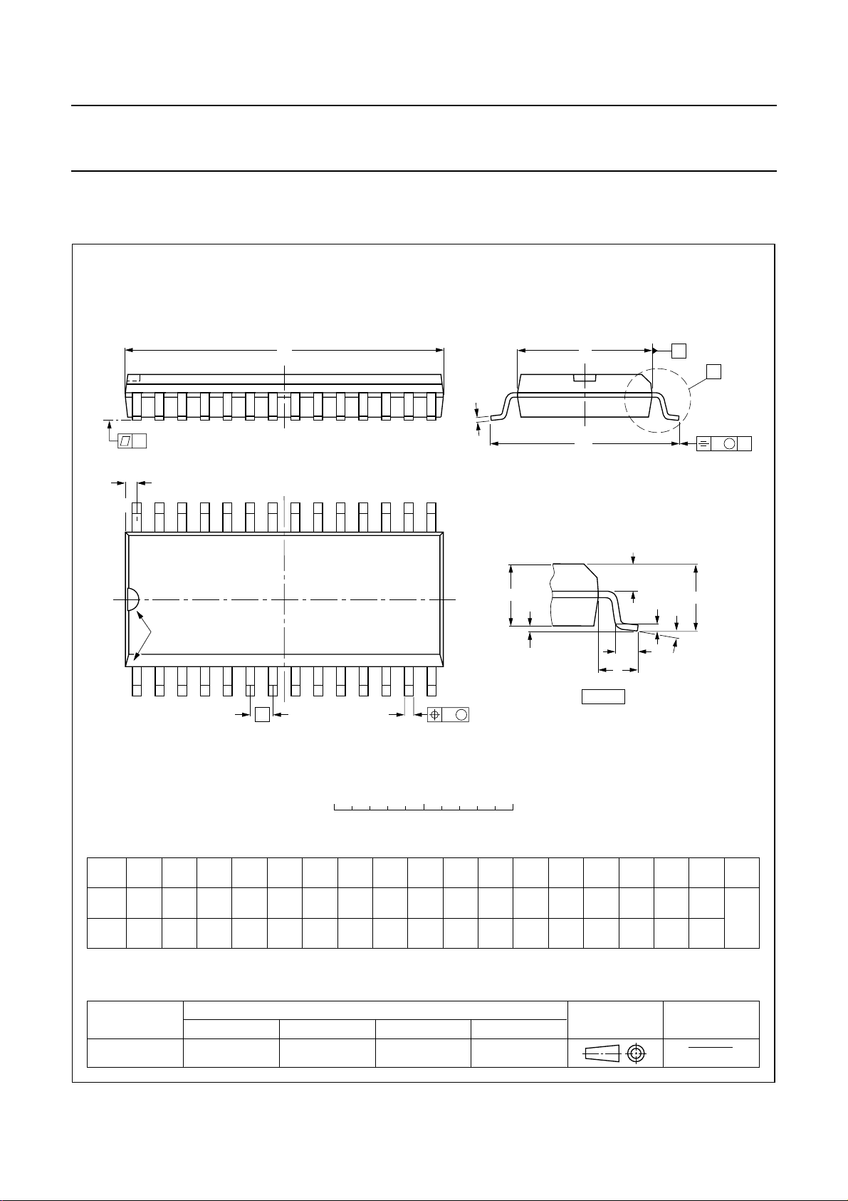
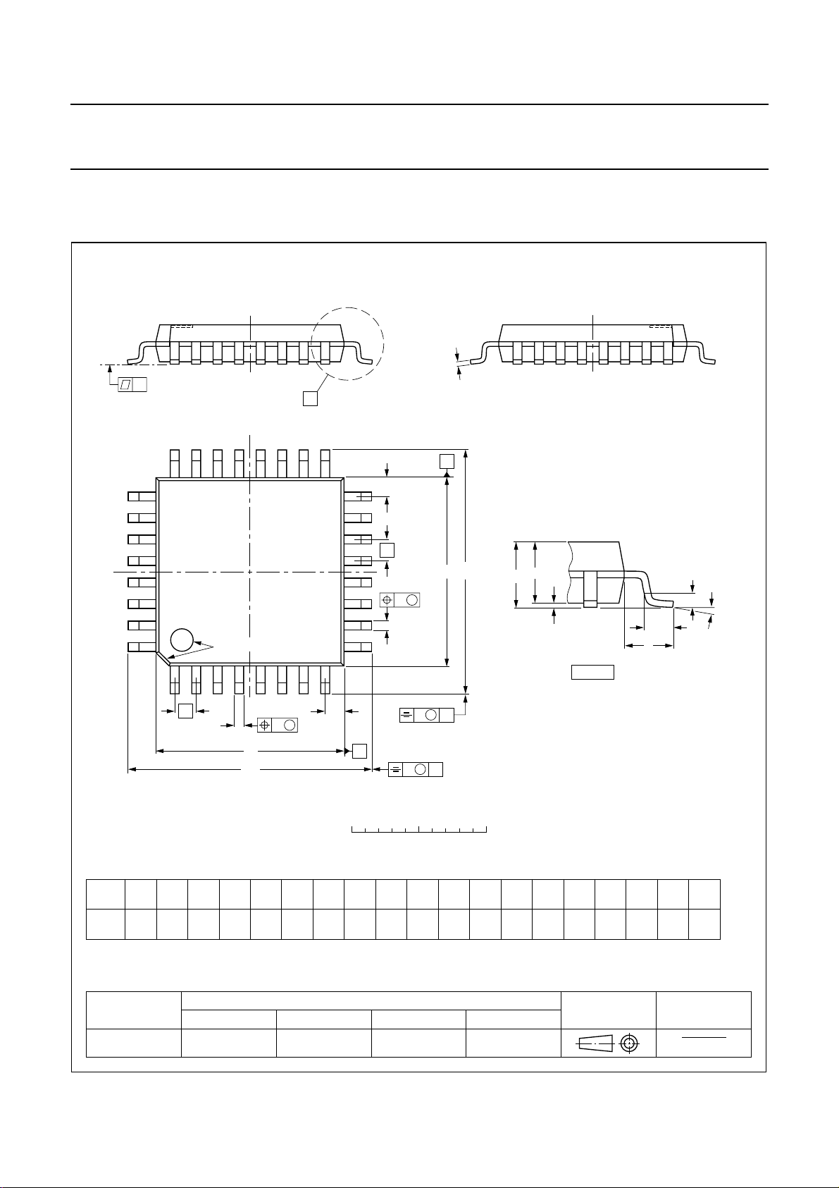
PACKAGE OUTLINES
SO28: plastic small outline package; 28 leads; body width 7.5 mm
D
c
y
Z
28
15
UMA1002
SOT136-1
E
H
E
A
X
v M
A
pin 1 index
1
e
0 5 10 mm
DIMENSIONS (inch dimensions are derived from the original mm dimensions)
UNIT
mm
inches
Note
1. Plastic or metal protrusions of 0.15 mm maximum per side are not included.
A
max.
2.65
0.10
A
1
0.30
0.10
0.012
0.004
A2A
2.45
2.25
0.096
0.089
0.25
0.01
b
3
p
0.49
0.32
0.36
0.23
0.019
0.013
0.014
0.009
(1)E(1) (1)
cD
18.1
7.6
17.7
7.4
0.71
0.30
0.69
0.29
14
w M
b
p
scale
eHELLpQ
1.27
0.050
10.65
10.00
0.419
0.394
1.4
0.055
Q
A
2
A
1
1.1
0.4
0.043
0.016
1.1
1.0
0.043
0.039
detail X
0.25
0.01
L
p
L
0.25 0.1
0.01
(A )
A
3
θ
ywv θ
Z
0.9
0.4
0.035
0.004
0.016
o
8
o
0
OUTLINE
VERSION
SOT136-1
IEC JEDEC EIAJ
075E06 MS-013AE
REFERENCES
1997 Jan 28 31
EUROPEAN
PROJECTION
ISSUE DATE
95-01-24
97-05-22
Page 32
Philips Semiconductors Product specification
Data processor for cellular radio
(DPROC2)
LQFP32: plastic low profile quad flat package; 32 leads; body 7 x 7 x 1.4 mm
c
y
X
24 17
25
16
Z
E
A
UMA1002
SOT358-1
e
w M
b
p
e
1.45
1.35
pin 1 index
b
p
D
H
D
0.25
w M
p
0.4
0.3
Z
(1) (1)(1)
cE
D
0.18
7.1
0.12
6.9
9
8
D
B
0 2.5 5 mm
(1)
7.1
6.9
v M
v M
scale
eH
H
9.15
0.8
8.85
32
1
DIMENSIONS (mm are the original dimensions)
mm
A
A1A2A3b
max.
0.20
1.60
0.05
UNIT
Note
1. Plastic or metal protrusions of 0.25 mm maximum per side are not included.
D
E
A
B
9.15
8.85
H
E
LL
E
A
0.75
0.45
A
p
2
A
1
detail X
Z
D
0.25 0.11.0 0.2
0.9
0.5
(A )
L
p
L
Zywv θ
E
0.9
0.5
3
θ
o
7
o
0
OUTLINE
VERSION
SOT358 -1
IEC JEDEC EIAJ
REFERENCES
1997 Jan 28 32
EUROPEAN
PROJECTION
ISSUE DATE
95-12-19
97-08-04
Page 33

Philips Semiconductors Product specification
Data processor for cellular radio
(DPROC2)
SOLDERING
Introduction
There is no soldering method that is ideal for all IC
packages. Wave soldering is often preferred when
through-hole and surface mounted components are mixed
on one printed-circuit board. However, wave soldering is
not always suitable for surface mounted ICs, or for
printed-circuits with high population densities. In these
situations reflow soldering is often used.
This text gives a very brief insight to a complex technology.
A more in-depth account of soldering ICs can be found in
our
“IC Package Databook”
Reflow soldering
Reflow soldering techniques are suitable for all QFP and
SO packages.
The choice of heating method may be influenced by larger
plastic QFP packages (44 leads, or more). If infrared or
vapour phase heating is used and the large packages are
not absolutely dry (less than 0.1% moisture content by
weight), vaporization of the small amount of moisture in
them can cause cracking of the plastic body. For more
information, refer to the Drypack chapter in our
Reference Manual”
Reflow soldering requires solder paste (a suspension of
fine solder particles, flux and binding agent) to be applied
to the printed-circuit board by screen printing, stencilling or
pressure-syringe dispensing before package placement.
Several techniques exist for reflowing; for example,
thermal conduction by heated belt. Dwell times vary
between 50 and 300 seconds depending on heating
method. Typical reflow temperatures range from
215 to 250 °C.
Preheating is necessary to dry the paste and evaporate
the binding agent. Preheating duration: 45 minutes at
45 °C.
(order code 9398 510 63011).
(order code 9398 652 90011).
“Quality
UMA1002
If wave soldering cannot be avoided, the following
conditions must be observed:
• A double-wave (a turbulent wave with high upward
pressure followed by a smooth laminar wave)
soldering technique should be used.
• The footprint must be at an angle of 45° to the board
direction and must incorporate solder thieves
downstream and at the side corners.
Even with these conditions, do not consider wave
soldering the following packages: QFP52 (SOT379-1),
QFP100 (SOT317-1), QFP100 (SOT317-2),
QFP100 (SOT382-1) or QFP160 (SOT322-1).
SO
Wave soldering techniques can be used for all SO
packages if the following conditions are observed:
• A double-wave (a turbulent wave with high upward
pressure followed by a smooth laminar wave) soldering
technique should be used.
• The longitudinal axis of the package footprint must be
parallel to the solder flow.
• The package footprint must incorporate solder thieves at
the downstream end.
ETHOD (QFP AND SO)
M
During placement and before soldering, the package must
be fixed with a droplet of adhesive. The adhesive can be
applied by screen printing, pin transfer or syringe
dispensing. The package can be soldered after the
adhesive is cured.
Maximum permissible solder temperature is 260 °C, and
maximum duration of package immersion in solder is
10 seconds, if cooled to less than 150 °C within
6 seconds. Typical dwell time is 4 seconds at 250 °C.
A mildly-activated flux will eliminate the need for removal
of corrosive residues in most applications.
Wave soldering
QFP
Wave soldering is not recommended for QFP packages.
This is because of the likelihood of solder bridging due to
closely-spaced leads and the possibility of incomplete
solder penetration in multi-lead devices.
1997 Jan 28 33
Repairing soldered joints
Fix the component by first soldering two diagonallyopposite end leads. Use only a low voltage soldering iron
(less than 24 V) applied to the flat part of the lead. Contact
time must be limited to 10 seconds at up to 300 °C. When
using a dedicated tool, all other leads can be soldered in
one operation within 2 to 5 seconds between
270 and 320 °C.
Page 34
Philips Semiconductors Product specification
Data processor for cellular radio
UMA1002
(DPROC2)
DEFINITIONS
Data sheet status
Objective specification This data sheet contains target or goal specifications for product development.
Preliminary specification This data sheet contains preliminary data; supplementary data may be published later.
Product specification This data sheet contains final product specifications.
Limiting values
Limiting values given are in accordance with the Absolute Maximum Rating System (IEC 134). Stress above one or
more of the limiting values may cause permanent damage to the device. These are stress ratings only and operation
of the device at these or at any other conditions above those given in the Characteristics sections of the specification
is not implied. Exposure to limiting values for extended periods may affect device reliability.
Application information
Where application information is given, it is advisory and does not form part of the specification.
LIFE SUPPORT APPLICATIONS
These products are not designed for use in life support appliances, devices, or systems where malfunction of these
products can reasonably be expected to result in personal injury. Philips customers using or selling these products for
use in such applications do so at their own risk and agree to fully indemnify Philips for any damages resulting from such
improper use or sale.
PURCHASE OF PHILIPS I
Purchase of Philips I
components in the I2C system provided the system conforms to the I2C specification defined by
Philips. This specification can be ordered using the code 9398 393 40011.
2
C COMPONENTS
2
C components conveys a license under the Philips’ I2C patent to use the
1997 Jan 28 34
Page 35

Philips Semiconductors Product specification
Data processor for cellular radio
(DPROC2)
UMA1002
NOTES
1997 Jan 28 35
Page 36

Philips Semiconductors – a worldwide company
Argentina: see South America
Australia: 34 Waterloo Road, NORTH RYDE, NSW 2113,
Tel. +61 2 9805 4455, Fax. +61 2 9805 4466
Austria: Computerstr. 6, A-1101 WIEN, P.O. Box 213,
Tel. +43 1 60 101, Fax. +43 1 60 101 1210
Belarus: Hotel Minsk Business Center, Bld. 3, r. 1211, Volodarski Str. 6,
220050 MINSK, Tel. +375 172 200 733, Fax. +375 172 200 773
Belgium: see The Netherlands
Brazil: see South America
Bulgaria: Philips Bulgaria Ltd., Energoproject, 15th floor,
51 James Bourchier Blvd., 1407 SOFIA,
Tel. +359 2 689 211, Fax. +359 2 689 102
Canada: PHILIPS SEMICONDUCTORS/COMPONENTS,
Tel. +1 800 234 7381
China/Hong Kong: 501 Hong Kong Industrial Technology Centre,
72 Tat Chee Avenue, Kowloon Tong, HONG KONG,
Tel. +852 2319 7888, Fax. +852 2319 7700
Colombia: see South America
Czech Republic: see Austria
Denmark: Prags Boulevard 80, PB 1919, DK-2300 COPENHAGEN S,
Tel. +45 32 88 2636, Fax. +45 31 57 1949
Finland: Sinikalliontie 3, FIN-02630 ESPOO,
Tel. +358 9 615800, Fax. +358 9 61580/xxx
France: 4 Rue du Port-aux-Vins, BP317, 92156 SURESNES Cedex,
Tel. +33 1 40 99 6161, Fax. +33 1 40 99 6427
Germany: Hammerbrookstraße 69, D-20097 HAMBURG,
Tel. +49 40 23 53 60, Fax. +49 40 23 536 300
Greece: No. 15, 25th March Street, GR 17778 TAVROS/ATHENS,
Tel. +30 1 4894 339/239, Fax. +30 1 4814 240
Hungary: see Austria
India: Philips INDIA Ltd, Shivsagar Estate, A Block, Dr. Annie Besant Rd.
Worli, MUMBAI 400 018, Tel. +91 22 4938 541, Fax. +91 22 4938 722
Indonesia: see Singapore
Ireland: Newstead, Clonskeagh, DUBLIN 14,
Tel. +353 1 7640 000, Fax. +353 1 7640 200
Israel: RAPAC Electronics, 7 Kehilat Saloniki St, TEL AVIV 61180,
Tel. +972 3 645 0444, Fax. +972 3 649 1007
Italy: PHILIPS SEMICONDUCTORS, Piazza IV Novembre 3,
20124 MILANO, Tel. +39 2 6752 2531, Fax. +39 2 6752 2557
Japan: Philips Bldg 13-37, Kohnan 2-chome, Minato-ku, TOKYO 108,
Tel. +81 3 3740 5130, Fax. +81 3 3740 5077
Korea: Philips House, 260-199 Itaewon-dong, Yongsan-ku, SEOUL,
Tel. +82 2 709 1412, Fax. +82 2 709 1415
Malaysia: No. 76 Jalan Universiti, 46200 PETALING JAYA, SELANGOR,
Tel. +60 3 750 5214, Fax. +60 3 757 4880
Mexico: 5900 Gateway East, Suite 200, EL PASO, TEXAS 79905,
Tel. +9-5 800 234 7381
Middle East: see Italy
Netherlands: Postbus 90050, 5600 PB EINDHOVEN, Bldg. VB,
Tel. +31 40 27 82785, Fax. +31 40 27 88399
New Zealand: 2 Wagener Place, C.P.O. Box 1041, AUCKLAND,
Tel. +64 9 849 4160, Fax. +64 9 849 7811
Norway: Box 1, Manglerud 0612, OSLO,
Tel. +47 22 74 8000, Fax. +47 22 74 8341
Philippines: Philips Semiconductors Philippines Inc.,
106 Valero St. Salcedo Village, P.O. Box 2108 MCC, MAKATI,
Metro MANILA, Tel. +63 2 816 6380, Fax. +63 2 817 3474
Poland: Ul. Lukiska 10, PL 04-123 WARSZAWA,
Tel. +48 22 612 2831, Fax. +48 22 612 2327
Portugal: see Spain
Romania: see Italy
Russia: Philips Russia, Ul. Usatcheva 35A, 119048 MOSCOW,
Tel. +7 095 755 6918, Fax. +7 095 755 6919
Singapore: Lorong 1, Toa Payoh, SINGAPORE 1231,
Tel. +65 350 2538, Fax. +65 251 6500
Slovakia: see Austria
Slovenia: see Italy
South Africa: S.A. PHILIPS Pty Ltd., 195-215 Main Road Martindale,
2092 JOHANNESBURG, P.O. Box 7430 Johannesburg 2000,
Tel. +27 11 470 5911, Fax. +27 11 470 5494
South America: Rua do Rocio 220, 5th floor, Suite 51,
04552-903 São Paulo, SÃO PAULO - SP, Brazil,
Tel. +55 11 821 2333, Fax. +55 11 829 1849
Spain: Balmes 22, 08007 BARCELONA,
Tel. +34 3 301 6312, Fax. +34 3 301 4107
Sweden: Kottbygatan 7, Akalla, S-16485 STOCKHOLM,
Tel. +46 8 632 2000, Fax. +46 8 632 2745
Switzerland: Allmendstrasse 140, CH-8027 ZÜRICH,
Tel. +41 1 488 2686, Fax. +41 1 481 7730
Taiwan: Philips Semiconductors, 6F, No. 96, Chien Kuo N. Rd., Sec. 1,
TAIPEI, Taiwan Tel. +886 2 2134 2870, Fax. +886 2 2134 2874
Thailand: PHILIPS ELECTRONICS (THAILAND) Ltd.,
209/2 Sanpavuth-Bangna Road Prakanong, BANGKOK 10260,
Tel. +66 2 745 4090, Fax. +66 2 398 0793
Turkey: Talatpasa Cad. No. 5, 80640 GÜLTEPE/ISTANBUL,
Tel. +90 212 279 2770, Fax. +90 212 282 6707
Ukraine: PHILIPS UKRAINE, 4 Patrice Lumumba str., Building B, Floor 7,
252042 KIEV, Tel. +380 44 264 2776, Fax. +380 44 268 0461
United Kingdom: Philips Semiconductors Ltd., 276 Bath Road, Hayes,
MIDDLESEX UB3 5BX, Tel. +44 181 730 5000, Fax. +44 181 754 8421
United States: 811 East Arques Avenue, SUNNYVALE, CA 94088-3409,
Tel. +1 800 234 7381
Uruguay: see South America
Vietnam: see Singapore
Yugoslavia: PHILIPS, Trg N. Pasica 5/v, 11000 BEOGRAD,
Tel. +381 11 625 344, Fax.+381 11 635 777
For all other countries apply to: Philips Semiconductors, Marketing & Sales Communications,
Building BE-p, P.O. Box 218, 5600 MD EINDHOVEN, The Netherlands, Fax. +31 40 27 24825
© Philips Electronics N.V. 1997 SCA53
All rights are reserved. Reproduction in whole or in part is prohibited without the prior written consent of the copyright owner.
The information presented in this document does not form part of any quotation or contract, is believed to be accurate and reliable and may be changed
without notice. No liability will be accepted by the publisher for any consequence of its use. Publication thereof does not convey nor imply any license
under patent- or other industrial or intellectual property rights.
Internet: http://www.semiconductors.philips.com
Printed in The Netherlands 437027/00/04/pp36 Date of release: 1997 Jan 28 Document order number: 9397 750 01602
 Loading...