

Page 1
TK83854
HIGH POWER FACTOR PREREGULATOR
FEATURES
■ Control Boost PWM to 0.99 Power Factor
■ Limit Line Current Distortion to < 5%
■ Worldwide Operation without Switches
■ Feed-Forward Line Regulation
■ Low Noise Sensitivity
■ Pin Compatible with UC2854, and UC3854
(Licensed Source)
DESCRIPTION
The TK83854 family of integrated circuits provide active
power factor correction for power systems that otherwise
would draw non-sinusoidal current from sinusoidal power
lines. These parts implement all the control functions
necessary to build a power supply preregulator capable of
optimally using available power-line current while
minimizing line-current distortion. To do this, the TK83854
contains a voltage amplifier, a precision analog multiplier/
divider, a current amplifier, and a fixed-frequency PWM. In
addition, the TK83854 contains a power MOSFET gate
driver, 7.5 V reference, line anticipator, load-enable
comparator, low supply detector, and overcurrent
comparator.
The TK83854 family uses average current-mode control to
accomplish fixed-frequency current control with stability
and low distortion. Unlike peak current-mode control,
average current control accurately maintains sinusoidal
line current without slope compensation.
FEATURES (CONT.)
■ Low Start-Up Supply Current
■ Fixed-Frequency PWM Drive
■ Low-Offset Analog Multiplier/Divider
■ 1 Amp Totem-Pole Gate Driver
■ Precision Voltage Reference
circuitry that supplies power to this device, the TK83854
family features low start-up supply current.
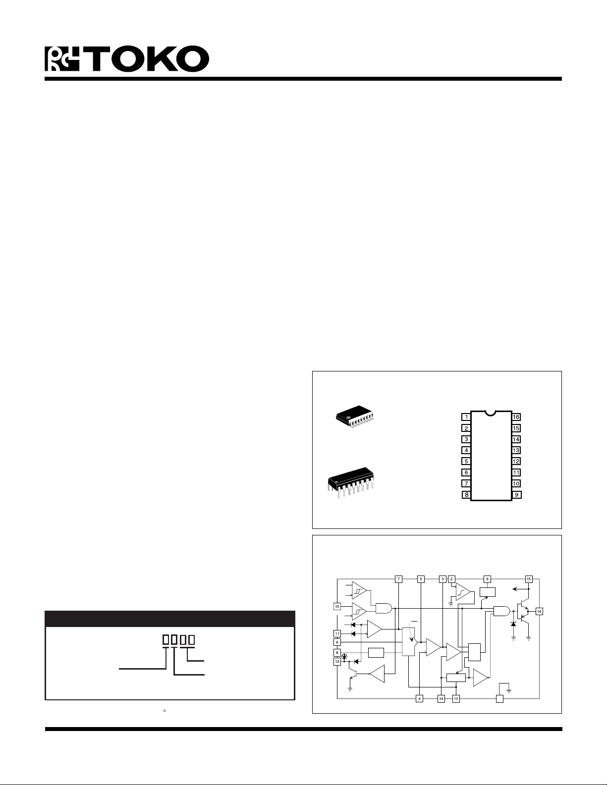
These devices are available in 16-pin plastic dual in-line
(DIP) and 16-pin surface mount (SOP) packages.
TK83854
83854
SOP-16
83854
DIP-16
CA
I
SENSE
MULT
VA
GND
PKLMT
OUT
OUT
IAC
OUT
V
RMS
GTDRV
V
CC
C
T
SS
R
SET
V
SENSE
ENA
V
ref
The TK83854's high reference voltage and high oscillator
amplitude minimize noise sensitivity while fast PWM
BLOCK DIAGRAM
elements permit chopping frequencies above 200 kHz.
IC POWER
1
V
CC
GT
DRV
15 V
The TK83854 can be used in systems with line voltages
that vary from 75 to 275 V and with line frequencies across
the 50 Hz to 400 Hz range. To reduce the burden on the
ORDERING INFORMATION
TK83854
Package Code
PACKAGE CODE
D: DIP-16
M: SOP-16
TEMP. RANGE
I: -40 TO +85
C
(OPTIONAL)
Tape/Reel Code
Extended Temp. Range
TAPE/REEL CODE
TL: Tape Left
MG: Magazine
V
SENSE
V
ENA
RMS
IAC
SS
16/10 V
2.5/2.25 V
7.5 V
R
RSQ
V
7-5 V
REF
RUN
ref
GND
MULT
VA
V
CC
14 µA
OUT
AB
IM =
C
A
B
2
C
X
I
SENSECTRSET
PKLMTCA
OUT
OUT
RUN
OSC
January 1999 TOKO, Inc. Page 1
Page 2

TK83854
ABSOLUTE MAXIMUM RATINGS
Supply Voltage ......................................................... 35 V
Power Dissipation TK83854D (Note 1) ..................... 1 W
Power Dissipation TK83854M (Note 2).............. 750 mW
GTDRV Current (Continuous) ................................. 0.5 A
GTDRV Current (50% Duty Cycle).......................... 1.5 A
Input Voltage (V
SENSE, VRMS
Input Voltage (ENA, I
) .................................... 11 V
, MULTOUT) .................. 11 V
SENSE
TK83854 ELECTRICAL CHARACTERISTICS
Test conditions: V
VI
SENSE
= 0 V, V
Temperature Range, unless otherwise specified.
LOBMYSRETEMARAPSNOITIDNOCTSETNIMPYTXAMSTINU
CC
OUT(CA)
= 18 V, R
= 3.5 V, V
= 15 k to GND, CT = 1.5 nF, PKLMT = 1 V, ENA = 7.5 V, V
SET
OUT(VA)
= 5 V, V
= 7.5 V, No load on SS, CA
SENSE
Input Voltage (PKLMT)............................................... 5 V
Input Voltage (IAC, R
Storage Temperature Range ................... -55 to +150 °C
Operating Temperature Range ......................0 to +70 °C
Extended Temperature Range................... -40 to +85 °C
Junction Temperature .......................................... 150 °C
Lead Soldering Temperature (10 s) ..................... 235 °C
OUT
, PKLMT) ........................ 10 mA
SET
= 1.5 V, IAC = 100 µA,
OUT
RMS
, V
, GTDRV, TA = Operating
ref
, VA
I
I
V
V
I
I
V
I
A
∆V
I
I
)FFO(CC
)NO(CC
OLVU
OLVU
ANE
ANE
)SMR(V
V
)NO(
CC
V
)FFO(
CC
)TSYH(ANE
V
SMR
FFOtnerruCylppuSV0=ANE5.10.2Am
NOtnerruCylppuS 0161Am
dlohserhTno-nruT5.410.615.71V
dlohserhTffo-nruT90111V
gnisiR,dlohserhTelbanE04.255.207.2V
siseretsyHdlohserhTelbanE02.052.003.0V
tnerruCtupnIelbanEV0=ANE0.5-2.0-0.5Aµ
tnerruCtupnIV
V5=0.1-10.0-0.1Aµ
SMR
REIFILPMAEGATLOV
)AV(SO
)AV(B
)AV(LO
)AV(CS
SS
V
ESNES
)AV(TUO
tnerruCSSV5.2=SS02-41-6-Aµ
tnerruCsaiB005-52-005An
niaGpmAegatloV07001Bd
egatloVtesffOpmAegatloVAV
gniwStuptuOpmAegatloV 8.5ot5.0V
tnerruCtiucriCtrohSpmAegatloVAV
V0=8-8Vm
TUO
V0=03-21-5-Am
TUO
REIFILPMATNERRUC
V
)AC(SO
I
)AC(B
A
∆V
Note 1: Power dissipation is 1 W when mounted as recommended. Derate at 8 mW/°C for operation above 25°C.
Note 2: Power dissipation is 750 mW when mounted as recommended. Derate at 3.3 mW/°C for operation above 25°C.
Gen. Note: All voltages with respect to GND (Pin 1).
Gen. Note: All currents are positive into the specified terminal.
I
ESNES
)AC(LO
)AC(TUO
tnerruCsaiB005-021-005An
niaGpmAtnerruC08011Bd
egatloVtesffOpmAtnerruC4-4Vm
gniwStuptuOpmAtnerruC 61ot5.0V
Page 2 January 1999 TOKO, Inc.
Page 3
TK83854 ELECTRICAL CHARACTERISTICS (CONT.)
Test conditions: V
VI
SENSE
= 0 V, V
Temperature Range, unless otherwise specified.
LOBMYSRETEMARAPSNOITIDNOCTSETNIMPYTXAMSTINU
CC
OUT(CA)
= 18 V, R
= 3.5 V, V
REIFILPMATNERRUC
= 15 k to GND, CT = 1.5 nF, PKLMT = 1 V, ENA = 7.5 V, V
SET
OUT(VA)
= 5 V, V
= 7.5 V, No load on SS, CA
SENSE
OUT
, VA
OUT
TK83854
= 1.5 V, IAC = 100 µA,
RMS
, V
, GTDRV, TA = Operating
ref
I
)AC(CS
V
)ESNESI(
I,egnaRtupnI
ESNES
TLUM,
WBGtcudorPWB-niaGpmAtnerruCT
tnerruCtiucriCtrohSpmAtnerruCAC
TUO
A
V0=03-21-5-Am
TUO
)3etoN(C°52=004008zHk
ECNEREFER
V
∆V
∆V
I
I
fer
V
)DAOL(fer
fer
V
)ENIL(fer
)CS(fer
fer
V
fer
egatloVecnerefeR
noitalugeRdaoLI<Am01-
noitalugeReniLV<V51
tnerruCtiucriCtrohSV
fer
I
fer
fer
T,Am0=
A
fer
CC
V0=05-82-21-Am
C°52=4.75.76.7V
.pmeTrevO,Am0=53.705.756.7V
Am0<51-551Vm
V53<01-201Vm
TIMILKAEP
V
)LP(SO
I
)LP(B
t
)LP(D
egatloVtesffOTMLKP 01-01Vm
tnerruCtupnITMLKPV1.0-=TMLKP002-001-Aµ
yaleD.porPVRDTGotTMLKP
Vm05-ot
Vm05morfgnillafTMLKP
REVIRDETAG
ot3.0-
5.2
V
571sn
V
)XAM(G
V
HG
V
)FFO(LG
egatloVtuptuOVRDTGmumixaMV<V81
HGIHegatloVtuptuOVRDTGV,ecruoSAm002
FFO,WOLegatloVtuptuOVRDTGV,kniSAm05
CC
CC
CC
daoLoN,V53<0.315.410.81V
V51=0.218.21V
V0=9.05.1V
kniSAm0020.12.2V
V
LG
I
)KP(G
t
t/
)G(R
)G(F
D
XAM
Note 3: Guaranteed by design; not 100% tested.
Gen Note: ENA input is internally clamped to approximately 14 V.
tnerruCVRDTGkaePdaoLFn010.1A
emiTllaF/esiRVRDTGdaoLFn153sn
,WOLegatloVtuptuOVRDTG
elcyCytuDmumixaMVRDTGAC
kniSAm011.04.0V
V7=59%
TUO
January 1999 TOKO, Inc. Page 3
Page 4
TK83854
TK83854 ELECTRICAL CHARACTERISTICS (CONT.)
Test conditions: V
VI
SENSE
= 0 V, V
Temperature Range, unless otherwise specified.
LOBMYSRETEMARAPSNOITIDNOCTSETNIMPYTXAMSTINU
REILPITLUM
I
)CAI(MO
CC
OUT(CA)
= 18 V, R
= 3.5 V, V
)DETIMIL
= 15 k to GND, CT = 1.5 nF, PKLMT = 1 V, ENA = 7.5 V, V
SET
OUT(VA)
= 5 V, V
tnerruCtuptuOreilpitluM
CAI(
= 7.5 V, No load on SS, CA
SENSE
R,Aµ001=CAI
TES
= 1.5 V, IAC = 100 µA,
OUT
, VA
OUT
RMS
, V
, GTDRV, TA = Operating
ref
k01=022-002-081-Aµ
tnerruCtuptuOreilpitluM
R(
oreZtnerruCtuptuOreilpitluMR,Aµ0=CAI
TES
TES
R,Aµ054=CAI
V
SMR
I
)CZ(MO
I
)TES(MO
)DETIMIL
V,Aµ05=CAI
V4=AV
V,Aµ001=CAI
V2=AV
I
MO
tnerruCtuptuOreilpitluM
V4=AV
V,Aµ002=CAI
V,Aµ003=CAI
V2=AV
V,Aµ001=CAI
V2=AV
k51=0.2-2.0-0.2Aµ
TES
SMR
SMR
SMR
SMR
SMR
,k51=
V6=AV,V1=
,V2=
,V2=
,V2=
,V1=
,V1=
082-552-022-Aµ
05-24-33-Aµ
83-72-21-Aµ
561-051-501-Aµ
052-522-051-Aµ
59-08-06-Aµ
KtnerruCniaGreilpitluM)4etoN(0.1-V
ROTALLICSO
f
CSO
V
PR
V
VR
Note 4: Multiplier gain constant (K) is defined by IOM = [K x I
C
T
C
T
ycneuqerFrotallicsO
edutilpmAkaeP-ot-kaePpmaR9.44.59.5V
egatloVyellaVpmaR8.01.13.1V
IAC
R
R
x (V
TES
TES
k51=645526zHk
k2.8=68201811zHk
OUT(VA)
- 1)] / V
RMS
2
.
Page 4 January 1999 TOKO, Inc.
Page 5

TK83854
PKLMT
NC
CA
OUT
10 k
MULT
IAC
OUT
NC
VA
OUT
V
RMS
10 k
10 k
TYPICAL PERFORMANCE CHARACTERISTICS
CURRENT AMPLIFIER GAIN AND
120
100
80
60
40
20
(dB)AND PHASE MARGIN ( )
OL(CA)
-20
A
PHASE vs. FREQUENCY
PHASE MARGIN
OPEN LOOP GAIN
0
0.1 1 10 100 1000 10000
FREQUENCY (kHz)
10 nF
10 nF
TEST CIRCUIT
GND
PKLMT
CA
OUT
I
100
10 k
10 k
120
100
80
60
40
20
(dB)AND PHASE MARGIN ( )
OL(VA)
-20
A
SENSE
MULT
IAC
VA
OUT
V
RMS
TA = TJ = 25 °C
VOLTAGE AMPLIFIER GAIN AND
PHASE vs. FREQUENCY
OPEN LOOP GAIN
0
0.1 1 10 100 1000 10000
FREQUENCY (kHz)
IM = (AB) / C
B
AC
PHASE MARGIN
7.5 V
GTDRV
R
V
SENSE
V
ENA
SET
V
0.1 nF
0.39 nF
CC
C
T
SS
ref
1.0 nF
100
0.01 nF
8.2 k
10 k
15 k
10 µF
1.0 nF
GATE DRIVE MAXIMUM DUTY
100
NC
V
CC
ENA
NC
0.1 µF
CYCLE vs. R
SET
95
90
85
80
DUTY CYCLE (%)
75
70
0 10 100
R
(kΩ)
SET
MULTIPLIER OUTPUT vs.
VOLTAGE ON MULTIPLIER
600
400
(µA)
200
MULTOUT
VA
= 5 V
OUT
V(rms) = 2 V
MULTOUT = 0 V
MULTOUT = 1 V
0
0 200 400 600 800
IAC (µA)
MULTOUT = 2 V
MULTOUT = 3 V
OSCILLATOR FREQUENCY
R
AND C
SET
1000
100
10
FREQUENCY (kHz)
1
10 nF
5 nF
1 10 100
R
(kΩ)
SET
VS.
T
100 pF
200 pF
500 pF
1 nF
2 nF
3 nF
GATE DRIVE RISE AND FALL TIMES
vs. LOAD CAPACITANCE
700
500
(ns)
F(G)
/ t
300
R(G)
t
FALL TIME
RISE TIME
100
0 .01 .02 .03 .04 .05
C
(µF)
LOAD
January 1999 TOKO, Inc. Page 5
Page 6

TK83854
TYPICAL PERFORMANCE CHARACTERISTICS (CONT.)
TA = TJ = 25 °C
MULTIPLIER OUTPUT vs. MULTIPLIER
INPUT (MULTOUT = 0 V)
300
V(rms) = 3 V
250
200
VA
OUT
= 5 V
150
VA
OUT
100
MULT OUT (µA)
50
VA
= 1.25 V
0
0 100 200 300 400 500
OUT
IAC (µA)
= 3 V
VA
OUT
= 2 V
MULTIPLIER OUTPUT vs. MULTIPLIER
INPUT (MULTOUT = 0 V)
160
V(rms) = 4 V
120
VA
= 5 V
OUT
VA
80
MULT OUT (µA)
VA
40
0
0 100 200 300 400 500
VA
IAC (µA)
OUT
OUT
VA
OUT
= 4 V
= 3 V
OUT
= 1.25 V
= 2 V
MULTIPLIER OUTPUT vs. MULTIPLIER
INPUT (MULTOUT = 0 V)
140
V(rms) = 5 V
100
VA
= 5 V
OUT
VA
OUT
60
MULT OUT (µA)
VA
= 1.25 V
20
OUT
0 100 200 300 400 500
IAC (µA)
= 3 V
Page 6 January 1999 TOKO, Inc.
Page 7

PIN DESCRIPTION
TK83854
GROUND PIN (GND)
All voltages are measured with respect to GND. VCC and
V
should be bypassed directly to GND with a 0.1 µF or
ref
larger ceramic capacitor. The timing capacitor discharge
current also returns to this pin, so the lead from the
oscillator timing capacitor to GND should also be as short
and as direct as possible.
PEAK LIMIT (PKLMT)
The threshold for PKLMT is GND. Connect this input to the
negative voltage on the current sense resistor as shown in
Figure 1. Use a resistor to V
to offset the negative current
ref
sense signal up to GND.
CURRENT AMPLIFIER OUTPUT (CA
OUT
)
This is the output of a wide-bandwidth op-amp that senses
line current and commands the Pulse Width Modulator
(PWM) to force the correct current. This output can swing
close to GND, allowing the PWM to force zero duty cycle
when necessary. The current amplifier will remain active
even if the IC is disabled.
CURRENT SENSE MINUS (I
SENSE
)
This is the inverting input to the current amplifier. This input
and the non-inverting input MULT
remain functional
OUT
down to and below GND. Care should be taken to avoid
taking these inputs below –0.5 V, because they are
protected with diodes to GND.
MULTIPLIER OUTPUT AND CURRENT SENSE PLUS
(MULT
OUT
)
The output of the analog multiplier and the non-inverting
input of the current amplifier are connected together at
MULT
also apply to MULT
current, this is a high impedance input similar to I
. The cautions about taking I
OUT
. As the multiplier output is a
OUT
below –0.5 V
SENSE
SENSE
, so
the current amplifier can be configured as a differential
amplifier to reject GND noise. Figure 1 shows an example
of using the current amplifier differentially.
INPUT AC CURRENT (IAC)
be used for sensing instantaneous line voltage. The nominal
voltage on IAC is 6 V, so in addition to a resistor from IAC
to rectified line, connect a resistor from IAC to V
resistor to V
is one-fourth of the value of the resistor to
ref
. If the
ref
the rectifier, then the 6 V offset will be cancelled, and the
line current will have minimal crossover distortion.
VOLTAGE AMPLIFIER OUTPUT (VA
OUT
)
This is the output of the op-amp that regulates output
voltage. Like the current amplifier, the voltage amplifier will
also stay active even if the IC is disabled with either ENA
or VCC. This means that large feedback capacitors across
the amplifier will stay charged through momentary disable
cycles. Voltage amplifier output levels below ~1 V will
inhibit multiplier output.
RMS LINE VOLTAGE (V(rms))
The output of a boost PWM is proportional to the input
voltage, so when the line voltage into a low-bandwidth
boost PWM voltage regulator changes, the output will
change immediately and slowly recover to the regulated
level. For these devices, the V(rms) input compensates for
line voltage changes if it is connected to a voltage
proportional to the RMS input line voltage. For best control,
the V
VOLTAGE REFERENCE OUTPUT (V
V
ref
voltage should stay between 1.5 V and 3.5 V.
RMS
)
ref
is the output of an accurate 7.5 V voltage reference.
This output is capable of delivering 10 mA to peripheral
circuitry and is internally short circuit current limited. V
ref
is
disabled and will remain at 0 V when VCC is low or when
ENA is low. Bypass V
to GND with a 0.1 µF or larger
ref
ceramic capacitor for best stability.
ENABLE (ENA)
ENA is a logic input that will enable the PWM output,
voltage reference, and oscillator. ENA also will release the
soft start clamp, allowing SS to rise. When unused, connect
ENA to a +5 V supply or pull ENA high with a 22 k resistor.
The ENA pin is not intended to be used as a high-speed
shutdown to the GTDRV output.
This input to the analog multiplier is a current. The multiplier
is tailored for very low distortion from this current input (IAC
to MULT
), so this is the only multiplier input that should
OUT
January 1999 TOKO, Inc. Page 7
Page 8

TK83854
PIN DESCRIPTION (CONT.)
VOLTAGE AMPLIFIER INVERTING OUTPUT (V
SENSE
This is normally connected to a feedback network and to
the boost converter output through a divider network.
OSCILLATOR CHARGING CURRENT AND MULTIPLIER
LIMIT SET (R
A resistor from R
SET
)
to ground will program oscillator
SET
charging current and maximum multiplier output. Multiplier
output current will not exceed 3.75 V divided by the resistor
from R
to ground.
SET
SOFT-START (SS)
SS will remain at GND as long as the IC is disabled or V
CC
is too low. SS will pull up to over 8 V by an internal 14 µA
current source when both VCC becomes valid and the IC is
enabled. SS will act as the reference input to the voltage
amplifier if SS is below V
. With a large capacitor from SS
ref
to GND, the reference to the voltage regulating amplifier
will rise slowly, and increase the PWM duty cycle slowly.
In the event of a disable command or a supply dropout, SS
will quickly discharge to ground and disable the PWM.
)
interaction between the gate impedance and the GTDRV
output driver that might cause the GTDRV output to
overshoot excessively. Some overshoot of the GTDRV
output is always expected when driving a capacitive load.
OSCILLATOR TIMING CAPACITOR (CT )
A capacitor from CT to GND will set the PWM oscillator
frequency according to this relationship:
f
= 1.25 / (R
OSC
SET
x CT)
POSITIVE SUPPLY VOLTAGE (VCC)
Connect VCC to a stable source of at least 20 mA above 17
V for normal operation. Also bypass VCC directly to GND to
absorb supply current spikes required to charge external
MOSFET gate capacitances. To prevent inadequate
GTDRV signals, these devices will be inhibited unless V
CC
exceeds the upper undervoltage lockout threshold and
remains above the lower threshold.
GATE DRIVER (GTDRV)
The output of the PWM is a totem pole MOSFET gate
driver on GTDRV. This output is internally clamped to
15 V so the IC can be operated with VCC as high as 35 V.
Use a series gate resistor of at least 5 ohms to prevent
Page 8 January 1999 TOKO, Inc.
Page 9

APPLICATION INFORMATION
TK83854
A 250 W PREREGULATOR
Figure 1 shows a typical application of the TK83854 as a
preregulator with high power factor and efficiency. The
assembly consists of two distinct parts, the control circuit
centering on the TK83854 and the power section.
The power section is a "boost" converter, with the inductor
operating in the continuous mode. In this mode, the duty
cycle is dependent on the ratio between input and output
voltages. Also, the input current has low switching frequency
ripple, which means that the line noise is low. Furthermore,
the output voltage must be higher than the peak value of
the highest expected AC line voltage, and all components
must be rated accordingly.
In the control section, the TK83854 provides PWM pulses
to the power MOSFET gate (GTDRV, Pin 16). The duty
cycle of this output is simultaneously controlled by four
separate inputs to the chip:
INPUT PIN # FUNCTION
V
11 Output DC Voltage
SENSE
IAC 6 Line Voltage Waveform
I
V
/MULT
SENSE
8 RMS Line Voltage
RMS
4/5 Line Current
OUT
Additional controls of an auxiliary nature are provided.
They are intended to protect the switching power MOSFET
from certain transient conditions, as follows:
INPUT PIN # FUNCTION
ENA 10 Start-up Delay
SS 13 Soft Start
PKLMT 2 Maximum Current Limit
Soft-Start (SS)
The voltage at Pin 13 (SS) can reduce the reference
voltage used by the error amplifier to regulate the output
DC voltage. With Pin 13 open, the reference voltage is
typically 7.5 V. An internal current source delivers
approximately 14 µA from Pin 13. Thus, a capacitor
connected between that pin and GND will charge linearly
from zero to 7.5 V in 0.54 x C seconds, with C expressed
in microfarads.
Peak Current Limit (PKLMT)
Use Pin 2 to establish the highest value of current to be
controlled by the power MOSFET. With the resistor divider
values shown in Figure 1, the 0.0 V threshold at Pin 2 is
reached when the voltage drop across the 0.25 Ω current
sense resistor is 7.5 V x 1.6 k / 10 k = 1.2 V, corresponding
to 4.8 A. A bypass capacitor from Pin 2 to ground is
recommended to filter out very high frequency noise.
CONTROL INPUTS
Output DC Voltage Sense (V
The threshold voltage for the V
)
SENSE
input is 7.5 V and the
SENSE
input bias current is typically -10 nA. The values shown in
Figure 1 are for an output voltage of 400 VDC. In this
circuit, the voltage amplifier operates with a constant low
frequency gain for minimum output excursions. The
0.047 µF feedback capacitor places a 15 Hz pole in the
voltage loop that prevents 120 Hz ripple from propagating
to the output current.
Line Waveform (IAC)
PROTECTION INPUTS
Enable (ENA)
The ENA input must reach 2.5 V before the V
ref
and
GTDRV outputs are enabled. This provides a means to
shut down the gate in case of trouble, or to add a time delay
at power up. A hysteresis gap of 200 mV is provided at this
terminal to prevent erratic operation. Undervoltage
protection is provided directly at Pin 15, where the on/off
thresholds are 16 V and 10 V, respectively.
In order to force the line current waveshape to follow the
line voltage, a sample of the power line voltage waveform
is introduced at Pin 6. This signal is multiplied by the output
of the voltage amplifier in the internal multiplier to generate
a reference signal for the current control loop.
This input is not a voltage, but a current (hence IAC). It is
set up by the 220 k and 910 k resistive divider (see Figure
1). The voltage at pin 6 is internally held at 6 V, and the two
resistors are chosen so that the current flowing into pin 6
varies from zero (at each zero crossing) to about 400 µA
at the peak of the waveshape. The following formulas were
January 1999 TOKO, Inc. Page 9
Page 10

TK83854
APPLICATION INFORMATION (CONT.)
used to calculate these resistors:
R
IAC
= V
PK(MAX)
/ 400 E - 6
= (260 VAC x 2 ) / 400 µA
= 910 k
R
REF
= R
/ 4 = 220 k
IAC
where VPK is the peak line voltage.
Line Current (I
/MULTOUT )
SENSE
The voltage drop across the 0.25 Ω current-sense resistor
is applied to Pins 4 and 5 as shown. The current-sense
amplifier also operates with high low-frequency gain, but
unlike the voltage amplifier, it is set up to give the currentcontrol loop a very wide bandwidth. This enables the line
current to follow the line voltage as closely as possible. In
the present example, this amplifier has a zero at about
500 Hz, and a gain of about 18 dB thereafter.
RMS Line Voltage (V
RMS
)
An important feature of the TK83854 preregulator is that it
can operate with a three-to-one range of input line voltages,
covering everything from low line in Japan (85 VAC) to
high line in Europe (255 VAC). This is done using line feedforward, which keeps the input power constant with varying
input voltage (assuming constant load power). To do this,
the multiplier divides the line current by the square of the
rms value of the line voltage. The voltage applied to Pin 8,
proportional to the average of the rectified line voltage (and
proportional to the RMS value), is squared in the TK83854,
and then used as a divisor by the multiplier block. The
multiplier output, at Pin 5, is a current that increases with
the current at Pin 6 and the voltage at Pin 7, and decreases
with the square of the voltage at pin 8.
With R
SET
= 15 k:
I
OM(MAX)
= -3.75 V / 15 k = -250 µA
It is also important to note that the multiplier output current
will never exceed twice IAC.
With the 3.9 k resistor from MULT
to the 0.25 Ω current
OUT
sense resistor, the maximum current in the current sense
resistor will be:
I
RCS(MAX)
Having selected R
resistor from MULT
= (-I
OM(MAX)
SET
x 3.9 k) / 0.25 Ω = -3.9 A
, the current sense resistor, and the
to the current sense resistor,
OUT
calculate CT for the desired PWM oscillator frequency from
the equation:
CT = 1.25 / (f
OSC
x R
SET
)
PWM Frequency
The PWM oscillator frequency in Figure 1 is 100 kHz. This
value is determined by CT at Pin 14 and R
R
should be chosen first because it affects the maximum
SET
at Pin 12.
SET
value of IOM according to the equation:
I
OM(MAX)
= -3.75 V / R
SET
This effectively sets a maximum PWM-controlled current.
Page 10 January 1999 TOKO, Inc.
Page 11

TH1
KC015L
R
25
910 K
F
1
6 A
C
1
0.47 µF
Q
3
ZVN4206A
R
9
91 K
C
12
0.1 µF
R
24 K
R
910 K
R
220 K
R
20 K
8
28
10
21
1KBU8J
R
470 K
1N4148
1N4746A
R
20
3 K
C
7
0.47 µF
TK83854
APPLICATION INFORMATION (CONT.)
D
9
IC POWER
1
R
511 K
R
10 K
15 V
17
V
OUT
385 VDC
18
R
16
20
V
CC
D
4
1N5821
GT
DRV
BR
~
+
D
R
27
8.2 M
V
SENSE
V
0.01 µF
11
ENA
IAC
RMS
C
MUR110
C
14
0.1 µF
C
17
0.1 µF
D
MUR110
V
CC
SS
10
0.47 µF
~
-
R
23
D
D
22
30 K
TIP50GE
Q
2
5
3
R
13
75 K
R
12
27 K
+
C
C
9
16
220 µF
1 µF
12
C
16 V
2.5 V
7.5 V
1N5406
L
5
14 µA
1
1 mH
D
13
R
7
240 K
C6 0.047 µF
VA
2
X
1N4148
OUT
MULT
IM =
A
B
C
R
3.9 K
AB
C
I
2
D
7
1N5817
OUT
LIMIT
0.25
C
13
68 pF
D
10
I
SENSE
C
C
1000 pF
R
1
C
15
1N4737
T
11
680 pF
R
24 K
6
RUN
1.6 K
OSC
R
3.9 K
R
PKLMT
D
MUR860
Q
1
IRF840
3
4
C3 270 pF
D8 1N5817
R
R
RSQ
R
SET
R
14
15 k
2
+
C
2
330 µF
C4 1 µF
10 K
29
V
ref
7-5 V
REF
RUN
GND
FIGURE 1: 250 W PREREGULATOR
January 1999 TOKO, Inc. Page 11
Page 12

TK83854
PACKAGE OUTLINE
SOP-16
DIP-16
Lot Number
16 9
7.5
81
10.3
2.3
+0.15
-0.05
0.4
16
1 8
Çl
0.12
Dimensions are shown in millimeters
Tolerance: x.x = ± 0.2 mm (unless otherwise specified)
e
1.27
0.1
0 ~ 0.3
2.8 max
9
Marking
6.35
0.76
1.7
e
1.27
Recommended Mount Pad
0.7
+
0.3
10.3
Country of Origin
0 ~ 10
Marking Information
9.53
1
e
+0.15
-0.05
0.25
Marking
TK83854 83854
19.05
0.3
+
3.3
4.2
0.3
+
3.2
e
2.54
Dimensions are shown in millimeters
Tolerance: x.x = ± 0.2 mm (unless otherwise specified)
0.5 min
0.5
M0.25
+0.15
e
-0.05
0.25
0 ~15
1
7.62
Toko America, Inc. Headquarters
1250 Feehanville Drive, Mount Prospect, Illinois 60056
Tel: (847) 297-0070 Fax: (847) 699-7864
TOKO AMERICA REGIONAL OFFICES
Midwest Regional Office
Toko America, Inc.
1250 Feehanville Drive
Mount Prospect, IL 60056
Tel: (847) 297-0070
Fax: (847) 699-7864
Western Regional Office
Toko America, Inc.
2480 North First Street , Suite 260
San Jose, CA 95131
Tel: (408) 432-8281
Fax: (408) 943-9790
Eastern Regional Office
Toko America, Inc.
107 Mill Plain Road
Danbury, CT 06811
Tel: (203) 748-6871
Fax: (203) 797-1223
Semiconductor Technical Support
Toko Design Center
4755 Forge Road
Colorado Springs, CO 80907
Tel: (719) 528-2200
Fax: (719) 528-2375
Visit our Internet site at http://www.tokoam.com
The information furnished by TOKO, Inc. is believed to be accurate and reliable. However, TOKO reserves the right to make changes or improvements in the design, specification or manufacture of its
products without further notice. TOKO does not assume any liability arising from the application or use of any product or circuit described herein, nor for any infringements of patents or other rights of
third parties which may result from the use of its products. No license is granted by implication or otherwise under any patent or patent rights of TOKO, Inc.
Page 12 January 1999 TOKO, Inc.
All Rights Reserved
IC-167-TK83854
0798O0.0K
Printed in the USA© 1999 Toko, Inc.
 Loading...