

Page 1
GND
FB/SD
V
ref
V
+
CAP
+
OSC
V
OUT
CAP
-
GND
FB/SD
V
ref
V
+
CAP
+
OSC
V
OUT
CAP
-
FEATURES
V
ref
CAP
+
+
-
BANDGAP
REFERENCE
CONTROL
Q
Q
OSC
1.25 V
CAP
-
V
OUT
DRIVE
DRIVE
DRIVE
DRIVE
V +
FB/SD
OSC
GND
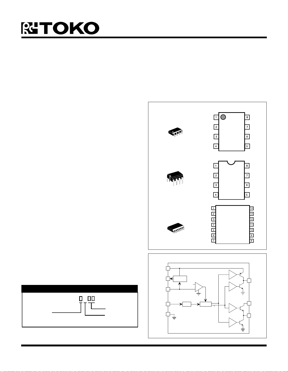
TK75018
SWITCHED CAPACITOR VOLTAGE
CONVERTER WITH REGULATOR
APPLICATIONS
■ 35 mA (typ.) Output Current
■ Operating Range 3.5 to 7 V
■ Reference and Error Amplifier for Regulation
■ External Shutdown
■ External Oscillator Synch
DESCRIPTION
The TK75018 is a monolithic switched capacitor converter
with feedback control. With just two capacitors, the TK75018
can create a negative voltage supply which tracks a
positive supply. As an alternative, the feedback pin can be
used to establish regulation at a desired voltage, and it can
also be used as a shutdown signal input. A single TK75018
can also be configured as a non-inverting step-up converter
or dual output voltage doubler.
With no external timing elements, the converter will selfoscillate at 25 kHz, nominal. This frequency can also be
user adjusted with a small capacitor or synchronized to
another oscillator.
Quiescent current is typically 2.5 mA. Standby current is
guaranteed less than 200 µA over the full operating
temperature and input voltage ranges.
■ Voltage Inverter
■ Negative Voltage Doubler
■ Voltage Regulator
■ Positive Voltage Doubler
TK75018
FB/SD
NC
CAP
GND
NC
CAP
NC
+
V
+
-
NC
OSC
V
ref
NC
NC
V
OUT
BLOCK DIAGRAM
ORDERING INFORMATION
TK75018 C
Package Code
PACKAGE CODE
D: DIP-8
M: SOP-8
V: TSSOP-14
May 1999 TOKO, Inc. Page 1
TEMPERATURE RANGE
C: -20 TO 80 °C
Tape/Reel Code
Temp. Range
TAPE/REEL CODE
TL: Tape Left
Page 2
TK75018
ABSOLUTE MAXIMUM RATINGS
Supply Voltage VIN For Doubler Conf. ....................... 7 V
Supply Voltage VIN For Regulating Conf................... 8 V
Power Dissipation TK75018M (Note 1).............. 600 mW
Power Dissipation TK75018D (Note 2) ............ 1000 mW
Storage Temperature Range ................... -55 to +150 °C
Operating Temperature Range .....................-20 to 80 °C
Junction Temperature .......................................... 150 °C
Lead Soldering Temperature (10 s) ..................... 235 °C
Power Dissipation TK75018V (Note 3) .............. 950 mW
TK75018 ELECTRICAL CHARACTERISTICS
Test conditions: V
SYMBOL PARAMETER TEST CONDITIONS MIN TYP MAX UNITS
I
CC(Reg)
I
CC(Inv)
V
CC
V
LOSS
R
OUT
f
OSC
V
ref
Mode
Reference Voltage
= 5.0 V, TA = Tj = Operating Temperature Range, Note 6 Configuration, unless otherwise specified.
IN
Supply Current Regulating I
Supply Current Inverting
= 0 mA, (Note 6) 2.5 3.5 mA
LOAD
= 0 mA 3.5 4.5 mA
I
LOAD
Supply Voltage Range Under Note 6 Conditions 3.5 7 V
= 1 mA, (Note 4) 0.35 0.55
I
OUT
Voltage Loss (VIN - V
Output Resistance
OUT
)
= 20 mA, (Note 4) 1 1.5
I
OUT
= 1 mA to 20 mA, (Notes 4,5)
∆I
OUT
32 54
Oscillator Frequency 3.5 V ≤ VIN ≤ 7 V, (Note 6) 15 25 35 kHz
= 25 °C 2.35 2.50 2.65 V
T
= T
j
A
= Operating Temp. Range 2.25 2.75 V
T
= T
j
A
V
V
Ω
V
OUT
Line Reg Line Regulation
LoadReg
LoadReg
I
STBY
R
OUT(Ref)
Note 1: Power dissipation is 600 mW when mounted as recommended. Derate at 4.8 mW/°C for operation above 25 °C.
Note 2: Power dissipation is 1000 mW when mounted as recommended. Derate at 8 mW/°C for operation above 25 °C
Note 3: Power dissipation is 950 mW when mounted as recommended. Derate at 7.6 mW/ °C for operation above 25 °C.
Note 4: Device is connected as an inverter, with pins 1, 6, and 7 unconnected; CIN = 2.2 µF tantalum, C
Note 5: Output resistance means the slope of the ∆V
Note 6: Device is connected as a positive to negative converter/regulator with R1 = 44.2 k, R2 = 154 k, C1 = 4.7 nF, C
CIN = 2.2 µF tantalum, C
Regulated Voltage Tj = 25 °C, I
Load Regulation @ 20 mA 1 mA ≤ I
1
Load Regulation @ 35 mA 1 mA ≤ I
2
Standby Current V
Reference Output
Resistance
of the curve.
= 33 µF tantalum.
OUT
3.5 V ≤ V
(Note 6)
= 0 V, (Note 6) 60 200 µA
PIN1
≤ 80 µA 350
V
ref
vs. ∆I
OUT
= 1 mA, (Note 6) -2.8 -3.0 -3.2 V
L
≤ 7 V, I
IN
≤ 20 mA, (Note 6) 20 150 mV
OUT
≤ 35 mA, (Note 6) 60 300 mV
OUT
curve, for output currents of 1 to 20 mA. This represents a linear approximation
OUT
= 1 mA,
L
15 80 mV
= 33 µF tantalum.
OUT
VIN
Ω
= 4.7 µF tantalum,
Page 2 May 1999 TOKO, Inc.
Page 3
C
V
OUT
(V)
-2.8
OUTPUT VOLTAGE
REGULATING @ 35 mA LOAD
VS.
TEMPERATURE
TEMPERATURE (°C)
-50 0 50 100
-3.0
-3.1
-3.2
-3.15
-3.05
-2.85
-2.95
-2.90
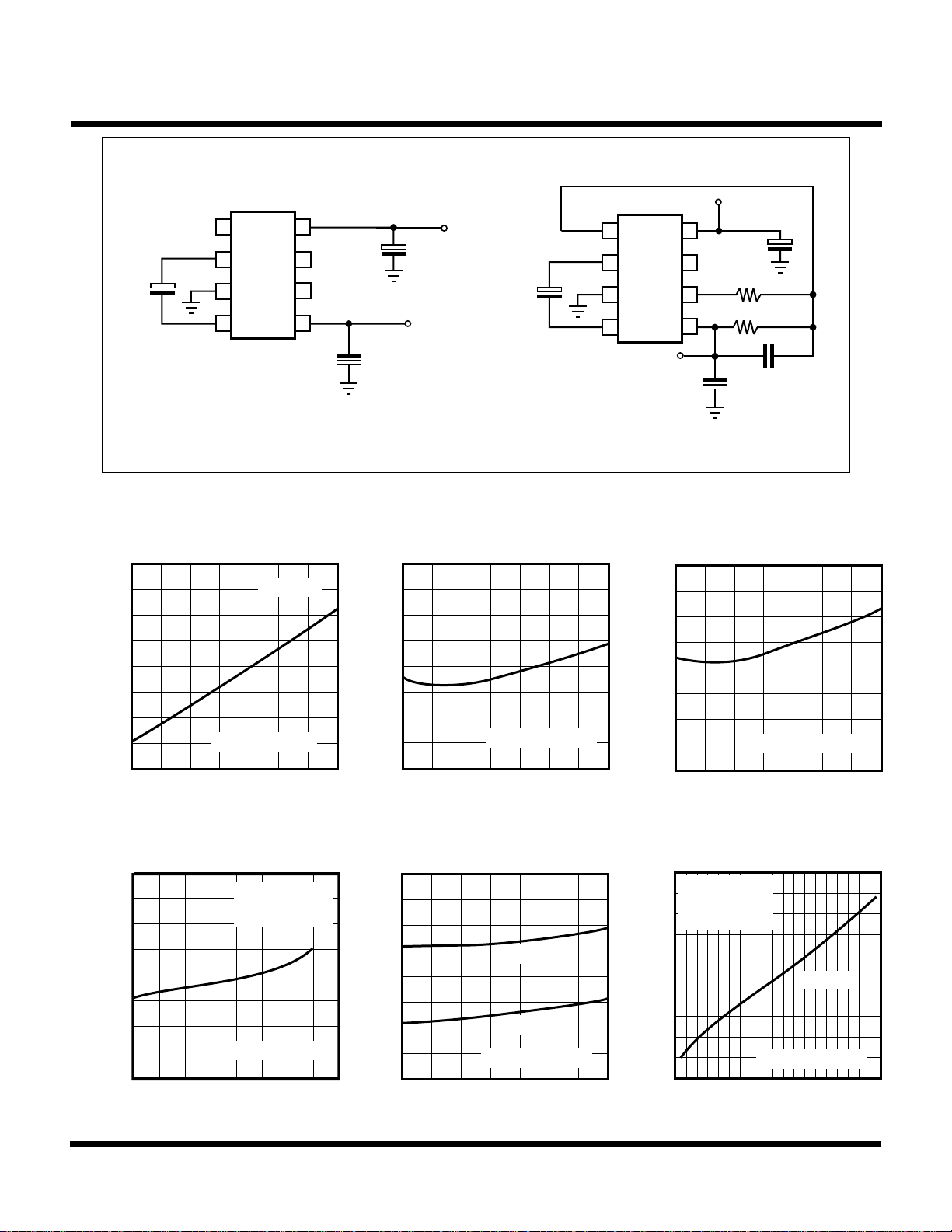
Note 6 Test Circuit
IN
2.2 µF
TK75018
TEST CIRCUITS
V
= 3.5 TO 7 V
IN
R
1
R
2
0.002 µF
+
4.7 µF
+
OUT
VIN = 3.5 to 6 V
+
4.7 µF
V
OUT
FB/SD
V +
C
+
2.2 µF
CAP +
IN
GND
V
ref
CAP -
V
OUT
V
OUT
C
OUT
33 µF
V +
+
CAP +
GND
CAP -
V
OUT
C
33 µF
+
NOTE 4 TEST CIRCUIT (Non Regulating)
REGULATING @ 0 mA LOAD
-2.8
-2.85
-2.9
-2.95
-3.0
-3.05
REGULATING MODE
-3.1
OUT
V
-3.15
-3.2
-50 0 50 100
-2.8
-2.85
(V)
-2.90
-2.95
-3.0
-3.05
-3.1
-3.15
OUT REGULATING MODE
V
-3.2
0 10 20 30 40
May 1999 TOKO, Inc. Page 3
TYPICAL PERFORMANCE CHARACTERISTICS
OUTPUT VOLTAGE
VS.
TEMPERATURE
V
IN
Note 6 Test Circuit
TEMPERATURE (°C)
OUTPUT VOLTAGE
OUTPUT CURRENT
V
= 5 V
IN
CIN = 2.2 µF
C
OUT
Note 6 Test Circuit
I
(mA)
OUT
= 5 V
VS.
= 33 µF
OUTPUT VOLTAGE
REGULATING @ 20 mA LOAD
VS.
TEMPERATURE
-2.8
-2.85
-2.9
-2.95
(V)
-3.0
OUT
V
-3.05
-3.1
-3.15
Note 6 Test Circuit
-3.2
-50 0 50 100
TEMPERATURE (°C)
OUTPUT VOLTAGE
TEMPERATURE
-3.4
-3.6
-3.8
-4.0
-4.2
-4.4
(V) NON REGULATING
-4.6
OUT
-4.8
V
Note 4 Test Circuit
-5.0
-50 0 50 100
TEMPERATURE (°C)
NOTE 6 TEST CIRCUIT (Regulating)
VOLTAGE LOSS
OUTPUT CURRENT
C
= 2.2 µF
IN
C
= 33 µF
OUT
VIN = 5 V
IL = 20 mA
IL = 5 mA
VS.
2
1.8
1.6
1.4
1.2
1
0.8
0.6
(V) NON REGULATING
0.4
LOSS
0.2
V
0
0 4 8 12 16 20 24 28 32 36
VS.
Tj = 25 °C
Note 4 Test Circuit
I
(mA)
OUT
Page 4

TK75018
f
(kH
)
TYPICAL PERFORMANCE CHARACTERISTICS (CONT.)
SUPPLY CURRENT vs.
TEMPERATURE @ 5 V
3
2.8
2.6
(mA)
CC
2.4
I
2.2
Note 6 Test Circuit
2
-50 0 50 100
TEMPERATURE (°C)
STANDBY CURRENT
100
90
80
70
60
(mA)
50
40
STBY
I
30
20
10
0
-50 0 50 100
TEMPERATURE
Note 6 Test Circuit
TEMPERATURE (°C)
VS.
SUPPLY CURRENT
INPUT VOLTAGE
IL = 03
2
(mA)
CC
I
1
Note 6 Test Circuit
0
0 6 12
VIN (V)
STANDBY CURRENT
INPUT VOLTAGE
120
V
100
80
(µA)
STBY
60
I
40
20
0 6 12
PIN1
Note 6 Test Circuit
VIN (V)
VS.
VS.
= 0 V
AVERAGE INPUT CURRENT
OUTPUT CURRENT
30
20
(mA)
IN(AVE)
10
I
Note 6 Test Circuit
0
0 15 30
I
(mA)
OUT
STANDBY THRESHOLD VS.
TEMPERATURE
0.6
V
0.4
(V)
TH(SA)
V
0.2
Note 6 Test Circuit
0
-50 0 50 100
TEMPERATURE (°C)
VS.
PIN1
MAXIMUM SWITCH CURRENT vs.
105
100
95
(mA)
SW
90
I
85
80
-50 0 50 100
TEMPERATURE
CAP+ Current to GND
TEMPERATURE (°C)
(V)
ref
V
2.65
2.60
2.55
2.50
2.45
2.40
2.35
REFERENCE VOLTAGE
TEMPERATURE
Note 6 Test Circuit
-50 0 50 100
TEMPERATURE (°C)
VS.
OSCILLATOR FREQUENCY VS.
TEMPERATURE
35
z
25
V
= 5 V
OSC
15
-75 -25 25 75 125
IN
Note 6 Test Circuit
TEMPERATURE (°C)
Page 4 May 1999 TOKO, Inc.
Page 5

TYPICAL PERFORMANCE CHARACTERISTICS (CONT.)
TK75018
OUTPUT VOLTAGE LOSS
OSCILLATOR FREQUENCY
INVERTER CONFIGURATION
2.0
CIN = 2.2 µF TANTALUM
C
= 33 µF TANTALUM
OUT
(V)
LOSS
1.0
V
0
1 10 100
I
OUT
Note 4 Test Circuit
f
(kHz)
OSC
VS.
=10 mA
(V)
LOSS
V
OUTPUT VOLTAGE LOSS
OSCILLATOR FREQUENCY
INVERTER CONFIGURATION
2.0
CIN = 22 µF TANTALUM
C
= 33 µF TANTALUM
OUT
1.0
0
1 10 100
THEORY OF OPERATION
As in any switched capacitor converter, the means of
conveying energy from input to output is done by charging
a capacitor between two potentials and then switching one
end of the capacitor to a different potential. By some
means of rectification, the other end of the capacitor is then
forced to dump charge into another capacitor at the
converter output, thereby conveying energy.
I
=10 mA
OUT
Note 4 Test Circuit
f
(kHz)
OSC
FIGURE 1: SWITCHED CAPACITOR CIRCUIT
VS.
OUTPUT VOLTAGE LOSS
INPUT CAPACITOR
1.0
INVERTER CONFIGURATION
C
= 33µF TANTALUM
OUT
0.8
f
= 25 kHz
OSC
I
0.6
(V)
LOSS
0.4
V
0.2
0
0 20 40 60 80 100
V
1
f
O
C
C
1
2
OUT
Note 4 Test Circuit
CIN (µF)
V
2
I
L
VS.
= 10 mA
In a simple example shown in Figure 1, a capacitor C1 has
one side tied to ground and another side charged by a
voltage source of potential V1. The non-grounded side of
C1 is then switched over to be connected to one side of a
If the potential V2 is sourcing a current IL, the charge will
have to be delivered at a rate:
capacitor C2, which is at potential V2 and referenced to
ground. V2 represents the output of the converter. The
initial charge on C1 is:
ƒ
= IL /∆q = IL / C1(V1 – V2)
O
Thus, the higher the frequency, the more current that can
q1 = C1 x V
1
be supported by the converter output.
All else being ideal, the effective losses in the converter in
When the switch changes over to the V2 side, C1 is
discharged from potential V1 to potential V2. After discharge
has occurred the charge on C1 is then:
the energy conveyance process is identical to that of a
circuit consisting of a resistor between the potentials V
and V2, with the same load at the output side. This
equivalent resistor is simply:
q2 = C1 x V
This means that the net transfer of charge which has
2
R
= (V1 – V2) / IL = 1 / (
EQUIV
ƒ
x C1)
O
occurred is:
∆q = q1 – q2 = C1 (V1 – V2)
May 1999 TOKO, Inc. Page 5
1
Page 6

TK75018
THEORY OF OPERATION (CONT.)
The illustration in Figure 2 represents an equivalent circuit
to the basic example of a switched capacitor circuit in
Figure 1.
V
1
R
EQUIV
C
2
V
2
I
L
FIGURE 2: SWITCHED CAPACITOR EQUIVALENT
CIRCUIT
The efficiency of the ideal converter is given by the output
power divided by the input power. Since the same current
flows out of each potential, the efficiency, η, is equal to the
ratio of V2 to V1.
PIN DESCRIPTIONS
FEEDBACK AND SHUTDOWN (FB/SD)
By configuring an error voltage divider into the FB/SD pin,
the TK75018 can be used to regulate the output voltage.
It is recommended that the parallel combination of the
divider resistors be greater than approximately 16 kΩ due
to the limited current available from the reference. The
Error Amplifier compares the FB/SD pin against an internal
1.25 V reference and limits the charge rate of CIN, thereby
limiting its peak charged voltage over a given clock period
and, thus, lowering the charge delivery rate to the output.
The characteristic frequency response of the converter
can be tailored by adjusting the ratio of C
OUT:CIN
recommended to keep it around 10:1. A “lead” capacitor
from the negative output to the feedback input is required
to maintain good light-load regulation; 2000 pF is
recommended, regardless of output voltage. For standard
configurations, the magnitude of the regulated voltage
must be less than that which can be achieved without
regulation, |V
OUT
| – V
. Higher regulated output voltages
LOSS
can be achieved by configuring a voltage doubler, at the
expense of maximum available output current.
When the FB/SD pin is pulled below the shutdown threshold
of ~0.45 V (e.g., via an open collector of an NPN transistor),
the reference is shut off and the switching action is
terminated. The drivers are set to allow both CIN and C
to discharge into the output load. The quiescent supply
current will drop to ~ 60 µA. If an error voltage divider is not
, but it is
OUT
Using equalities established above we find:
η = V2 / V1 = {V1 – [IL / (ƒ
x
C1)]} / V1 = 1 – [IL / (ƒ
O
x
C
x
O
V1)]
1
The last term in the equality string shows that efficiency
can be improved by increasing frequency or the value of
C1. Limitations of the circuit and components tend to cause
losses which increase with increasing frequency. Therefore,
at some point in the frequency spectrum losses will be
minimized. Hence, the oscillator of the TK75018 is designed
to run in the frequency band where losses are minimized.
Since the user will primarily be interested in maintaining a
given output voltage, losses are characterized in terms of
the voltage loss.
being used, the TK75018 will automatically restart when
the shutdown signal is removed. If such a divider is being
used, the current through the divider may be sufficient to
keep the device in shutdown until C
is fully discharged,
OUT
since the reference to the amplifier has collapsed during
the shutdown. Although C
is discharged fairly quickly
OUT
(allowing a quick restart), this recycling delay may not be
acceptable in some applications. This recycling delay can
be bypassed by injecting a positive start-up pulse into the
SD/FB pin (see Figure 3). This might be readily configured,
for example, as a TTL level signal which is diode coupled
into the divider. A resistor should be chosen to limit the
voltage pulse injection magnitude to 0.7 to 1.1 V. A pulse
width of ≥ 100 µs is required to guarantee a successfully
coupled start-up signal.
+
V
ref
C
OUT
33 µF
TANTALUM
4.7 µF
R
1
R
2
+
V
OUT
V
RESTART
SHUTDOWN
IN
V +
FB/SD
CAP +
+
CAP -
V
C
IN
2.2 µF
TANTALUM
OUT
GND
FIGURE 3: FEEDBACK AND SHUTDOWN
Page 6 May 1999 TOKO, Inc.
Page 7

PIN DESCRIPTIONS (CONT.)
TK75018
INPUT CAPACITOR CHARGING PINS (CAP+/CAP- )
The positive driving pin of CIN (CAP +) charges the positive
node of the capacitor to VIN during tCH and pulls it down to
ground during t
. The negative driving pin of C
DIS
IN
(CAP -) pulls the negative node of the capacitor to ground
during tCH and is driven into the output during t
DIS
.
CIRCUIT GROUND (GND)
All potentials are referenced to this ground unless otherwise
noted.
OUTPUT VOLTAGE (V
OUT
)
In most applications, a capacitor must be placed from this
pin to ground to integrate the charge pulses delivered by
CIN. A minimum of ten times CIN is recommended. Since
the output voltage serves as the substrate inside the IC,
the design must ensure that this pin is never raised to a
higher potential than ground. This phenomenon will tend to
occur when a positive-supply-to-negative-supply load is
present at the converter output. A circuit, such as the one
shown in Figure 4, is recommended. Under normal
operation, the transistor will appear as a short circuit. But
the sink current will be cut off from the output pin if the
voltage starts to approach ground. The resistor is chosen
to keep the transistor saturated under all steady-state
operating conditions.
+
V
I
L
V +
+
C
IN
CAP +
GND
CAP -
V
OUT
LOAD
C
OUT
+
FIGURE 4: POSITIVE REFERENCED LOAD
The equation below can be used to calculate the values of
the feedback resistors (R1 and R2) needed to achieve a
desired output voltage.
|V
|
R2 = R1 +1 where R1 ≥ 24 kΩ
(
OUT
1.2 V
)
REFERENCE VOLTAGE (V
ref
)
This pin provides a nominal 2.5 V buffered reference for
external use. Normal output current should be kept below
~160 µA.
OSCILLATOR PROGRAMMING (OSC)
This pin can be used to alter the nominal 25 kHz frequency
of the internal oscillator. An internal timing capacitor of
~150 pF is alternately charged during
during
t
with a 7 µA current source to fixed threshold
DIS
t
and discharged
CH
levels. Adding an external capacitor from the OSC pin to
ground will parallel the 150 pF capacitor to slow down the
clock period. Adding a small external capacitor from the
OSC pin to the CAP+ pin will source/sink extra charge into/
out-of the internal timing capacitor to speed up the transition
between thresholds and thereby raise the oscillator
frequency. It is recommended that, in the latter
configuration, the capacitor be kept below ~30 pF.
Synchronization of multiple TK75018s can be accomplished
by adding pull-up resistors from the OSC pin to the
reference voltage and using an open collector from an
NPN transistor to provide the discharge. The NPN is then
driven by a clocking pulse, and the same pulse can be
used to drive multiple devices in the same configuration.
It is not recommended to pull the OSC pin high with a lowimpedance source. To synchronize and regulate with
multiple devices, an external reference can be used as the
reference point for the error voltage divider, thus allowing
the internal reference to be used as the pull-up point for the
OSC pin.
INPUT VOLTAGE (V+)
The input voltage is used to charge CIN during the time t
CH
during each clock period. CIN is then discharged into the
output capacitor during time t
. During tCH, the input
DIS
current will be approximately 2.2 times the output current.
During t
, the input current will be approximately 0.2
DIS
times the output current. A low ESR bypass capacitor will
average out the varying current seen by the input supply yielding an average input current of approximately 1.1
times the output current. The bypass capacitor should be
placed as near to the TK75018 as possible to disallow
inductive spikes on the supply rail of the IC. A minimum of
2 µF is recommended.
May 1999 TOKO, Inc. Page 7
Page 8

TK75018
)
SOP-8
85
PACKAGE OUTLINE
0.76
1.27
5.4
1
e
e
3.9
1.27
Recommended Mount Pad
TSSOP-14
14
0.35
1.0
Marking
8
4.8
DIP-8
1
4
4.89
e
0.42
Dimensions are shown in millimeters
Tolerance: x.x = 0.2 mm (unless otherwise specified
1.27
l
0.12
8
1
Dimensions are shown in millimeters
Tolerance: x.x =
0.1
e
0.3
+
1.45
1.64
0 ~ 0.25
5
4
9.5
2.54
0.46
0.2 mm (unless otherwise specified)
AAAAA
0.5
0 ~ 10
0.2
+
0.3
6.07
Marking
Lot Number
6.4
Country of Origin
0.3
+
3.3
3.8
0.3
+
3.3
0.5 min
+ 0.15
- 0.05
0.25
+ 0.15
- 0.05
0.25
e1
0 ~15
7.62
M
1
Product Code TK75018
YYY
Lot. No.
+0.15
-0.15
0.25
Dimensions are shown in millimeters
Tolerance: x.x = 0.2 mm (unless otherwise specified)
4.4
7
5.0
0.9
1.2 max
e
0.12
0 ~ 0.15
0.65
0.1
M
Marking Information
e
0.65
Recommended Mount Pad
0 ~ 10
0.50
+
0.3
6.4
+0.15
-0.15
0.15
Toko America, Inc. Headquarters
1250 Feehanville Drive, Mount Prospect, Illinois 60056
Tel: (847) 297-0070 Fax: (847) 699-7864
TOKO AMERICA REGIONAL OFFICES
Midwest Regional Office
Toko America, Inc.
1250 Feehanville Drive
Mount Prospect, IL 60056
Tel: (847) 297-0070
Fax: (847) 699-7864
Western Regional Office
Toko America, Inc.
2480 North First Street , Suite 260
San Jose, CA 95131
Tel: (408) 432-8281
Fax: (408) 943-9790
Eastern Regional Office
Toko America, Inc.
107 Mill Plain Road
Danbury, CT 06811
Tel: (203) 748-6871
Fax: (203) 797-1223
Semiconductor Technical Support
Toko Design Center
4755 Forge Road
Colorado Springs, CO 80907
Tel: (719) 528-2200
Fax: (719) 528-2375
Visit our Internet site at http://www.tokoam.com
The information furnished by TOKO, Inc. is believed to be accurate and reliable. However, TOKO reserves the right to make changes or improvements in the design, specification or manufacture of its
products without further notice. TOKO does not assume any liability arising from the application or use of any product or circuit described herein, nor for any infringements of patents or other rights of
third parties which may result from the use of its products. No license is granted by implication or otherwise under any patent or patent rights of TOKO, Inc.
Page 8 May 1999 TOKO, Inc.
© 1999 Toko, Inc.
All Rights Reserved
IC-xxx-TK75018
0798O0.0K
Printed in the USA
 Loading...