

Page 1
Features and Benefits
TH8082
Single LIN Bus
Transceiver
www.melexis.com
Page 1 Data Sheet Rev 1.0 June 2001
Single wire LIN transceiver
Compatibl e to LIN Protoc ol S pec ification, Rev. 1.1
Compatible to ISO9141 functions
Control Output for voltage regulator
Up to 20 kbps bus speed
Low RFI due to slew rate contr ol
Fully integrated receiver filter
Protection against load dump, jump start
Bus terminals proof against short-cir c uits and transients in the
automotiv e environment
Very low (25 µA) typical power consum ption in sleep mode
Thermal ov erl oad and short ci r c uit pr otection
High impendance Bus pin in case of loss of ground and undervoltage c ondition
± 4kV ESD protecti on on bus pin
Ordering Information
Part No. Temperature Rang e Package
TH8082 JDC -40ºC...125ºC SOIC8, 150mil
General Descri ption
The TH8082 is a physical layer device for a single wire
data link capable of operating in applications where high
data rate is not required and a lower data rate can
achieve cost reductions in both the physical media components and in the microprocessor which use the network. The TH8082 is designed in accordance to the
physical layer definition of the LIN Protocol Specification , Rev. 1.2 . The IC furthermore can be used in
ISO9141 systems.
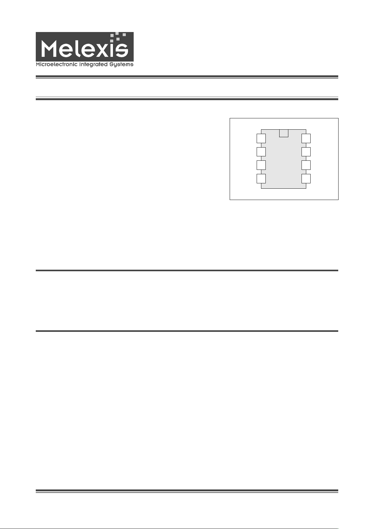
TH8082
1
2
3
4
8
7
6
5
RxD
GNDTxD
EN
INH
VS
BUSVCC
Pin Diagram
SOIC8NB
Because of the very low current consumption of the
TH8082 in the recessive state it’s particularly suitable for
ECU applications with hard standby current requirement s .
An advanced sleep mode capability allows
a shutdown of the whole appli cation . The incl uded
wake-up function detects incoming dominant bus
messages and enables the v oltage regulator.
Page 2

TH8082
Single LIN Transceiver
www.melexis.com
Page 2 Data Sheet Rev 1.0 June 2001
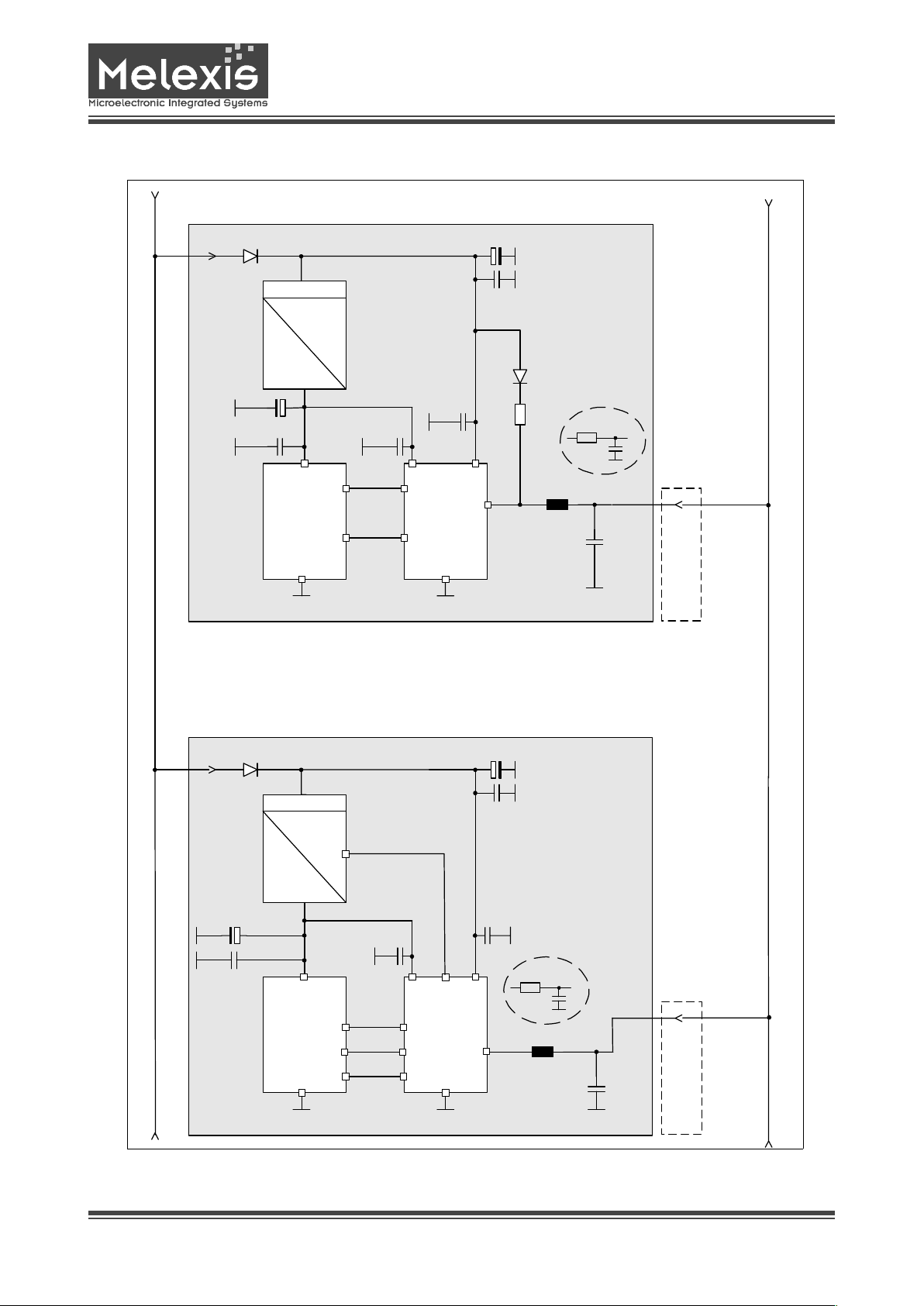
Functional Diagram
SLEW RATE
BUS Driver
Biasing &
Bandgap
VS
internal Supply
&
References
Receive
Comparator
Input
Filter
TH8082
Thermal
Protection
BUS
GND
POR
MODE
CONTROL
TxD
RxD
VCC
EN
INH
Wake-up
Filter
Figure 1 - Block Diagram
Page 3
TH8082
Single LIN Transceiver
www.melexis.com
Page 3 Data Sheet Rev 1.0 June 2001
Functional Description
After power on the chip automatically enters the V
BAT
-
stanby mode . In this intermediate mode the INH output
will becom e HIGH (V
S
) and therefore the voltage regula-
tor will provi de the V
CC
- supply . The transceiver will
remain the V
BAT
-stanby mode until the controller sets it to
normal operation ( EN = High ) . Only in this mode bus
communication is possible. The TH8082 switches itself in
the V
BAT
-stanby mode if V
CC
is missing or below the
threshold.
The sleep mode ( EN = LOW) can only be reached from
normal mode and permits a very low power consumtion
because the transceiver and even the external voltage
regulator get disabled. If the V
CC
has been s witch ed of f a
wake-up request from the bus line will cause the TH8082
to enter the V
BAT
-stanby mode (VCC is present again) and
sets the RxD output to low until the device enters the
normal operation mode (active LOW interrupt at RxD). If
the INH pin is not connect ed to th e regulator or the inh ibitabl e extern al regu lator i s not the on e that pr ovides t he
V
CC
– supply, the normal mode is directly accessilble by
a logic high on the EN pin.
In order to prevent an unintended wake-up caused by
distur bances of th e autom otiv environment in coming
dominant signals from the bus have to exceed the wake–
up delay time.
EN VCC Comment INH RxD
0 0 V
BAT
-standby , power on Vs 0
0 1 V
BAT
-standby , VCC on , wake up condition after
power on
Vs Active LOW
wake-up interrupt
1 1 Normal mode , VCC on Vs 1 = recessive bus
0 = dominant bus
1 0 V
BAT
-standby , VCC missing (VCC<V
CCUV
) Vs V
CC
0 0 Sleep mode, switch to V
BAT
-standby in case of
wake-up request
floating Active LOW wake-up inter-
rupt if V
CC
is p resent
0 1 Sleep mode, regulator not disabled, switch to
V
BAT
-standby in case wake-up request, directly
switc h to n o rmal mo d e with EN = 1
floating Active LOW
wake-up interrupt
Mode Control of TH8082
Page 4
TH8082
Single LIN Transceiver
www.melexis.com
Page 4 Data Sheet Rev 1.0 June 2001
Application Circuit
100nF
TH8082
RxD
V
BAT
Voltage regulator
+5V
V
BAT
2.2uF1N4001
µP
VCC
ECU connector to
Single Wire LIN
Bus
BUS
33µH
82pF
TxD
VS
100nF
TH8080
[1]
RxD
V
BAT
Voltage regulator
+5V
V
BAT
2.2uF1N4001
µP
VCC
ECU connector to
Single Wire LIN
Bus
BUS
33µH
82pF
TxD
GND
VS
Car Battery
SLAVE
ECU
MASTER
ECU
100nF
GND
GNDGND
100nF
100nF
100nF
100nF
100nF
LIN BUS
EN
100p
10
optional
100p
10
optional
INH
INH
[1] TH8080 - low cost transceiver without INH control
Figure 2 - Application Circuit
Page 5

TH8082
Single LIN Transceiver
www.melexis.com
Page 5 Data Sheet Rev 1.0 June 2001
Operating Conditions
Electrical Specification
All voltages are referenced to ground (GND). Positive
currents flow into the IC. The absolute maximum ratings
given in the table below are limiting values that do not
lead to a permanent damage of the device but exceeding
any of these limits may do so. Long term exposure to limiting values may affect the reliability of the device. Reliable operation of the TH8082 is only specified within the
limits shown in ”Operating conditions”.
Absolute Maximum Ratings
Parameter Symbol Min Max Unit
Battery voltage VS 6 18 V
Supply voltage V
CC
4.5 5.5 V
Operating am bient temp erature T
A
-40 +125 °C
Junction temperature
[1]
T
Jc
+150 °C
______________________________
Parameter Symbol Conditions Min. Max. Unit
Batterry Supply Voltage V
S
t < 1 min -0.3 + 30 V
-0.3 +7
Load dump; t<500ms +40
Transient supply voltage V
S.tr1
ISO 7637/1 pulse 1
[1]
-150 V
ISO 7637/1 pulses 2
[1]
+100
Transient supply voltage V
S.tr3
ISO 7637/1 pulses 3A, 3B -150 +150 V
BUS voltage V
BUS
t < 500 ms, VS = 20 V
V
S
= 20 V
-20
-40
+40 V
Transient bus voltage V
BUS.tr1
ISO 7637/1 pulse 1
[2]
-150 V
Transient bus voltage V
BUS.tr2
ISO 7637/1 pulses 2
[2]
+100 V
Transient bus voltage V
BUS.tr3
ISO 7637/1 pulses 3A, 3B
[2]
-150 +150 V
DC voltage on pins TxD, RxD V
DC
-0.3 +7 V
ESD capability of pin BUS ESD
BUSHB
Human body model, equivalent -4 +4 kV
ESD capability of any other pins ESD
HB
Human body model, equivalent -2 +2 kV
Maximum latch – up fr ee current at any Pin I
LATCH
-500 +500 mA
Maximum power dissipation P
tot
At T
amb
= +125 °C 197 mW
Thermal impedance
Θ
JA
in free air 152 K/W
Storage temp erature T
stg
-55 +150 °C
Junction temperature T
vj
-40 +150 °C
Supply Voltage
Short-term supply voltage
V
CC
V
S.ld
V
V
Transient supply voltage V
S.tr2
V
Page 6

TH8082
Single LIN Transceiver
www.melexis.com
Page 6 Data Sheet Rev 1.0 June 2001
Static Characteristics
(V
S
= 6 to 18V, VCC= 4.5 to 5.5V, TA = -40 to +125°C, unles s otherwi se specified)
All voltages are referenced to ground (GND), positive currents are flow into the IC.
Parameter Symbol Conditions Min Typ Max Unit
PIN VS,VCC
Supply current, dominant I
Sd
VS = 18V,VCC = 5.5V, TxD=L 50 µA
Supply current, dominant I
CCd
VS = 18V,VCC = 5.5V, TxD =L 1 mA
Supply current, recessive I
Sr
VS = 18V,VCC = 5.5V TxD = H 8 20 µA
Supply current, recessive I
CCr
VS = 18V,VCC = 5.5V TxD = H 20 30 µA
V
CC
undervoltage lockout V
CC_UV
EN = H, TxD = L 2.75 4.3 V
Supply current, sleep mode I
Ss1
VS = 18V,VCC = 0V TxD open 25 50 µA
PIN BUS / TRANSMITTER
Bus output voltage, dominant V
ol_BUS
TxD=L , I
BUS
= 40mA,VS > 7.3V 1.2 V
Bus output voltage, recessive V
oh_BUS
TxD=open
0.8*
V
S
+ 0.7
V
Bus short circuit current I
BUS_SHORT
TxD=L , V
BUS
> 1.2V, VS > 7.3V 40 200 mA
Bus input current, recessive I
BUS_leakp
TxD open ,V
BUS
= Vs -20 20 µA
Bus reverse polarity curr., rec. I
BUS_leakn
Loss of GND ,VS =12V, V
BUS
=0 -1 1 mA
Bus pull up resistor R
BUS_pu
TxD open, V
BUS
=0 20 30 47
kΩ
PIN BUS / RECEIVER
Bus input threshold, recessive
to dominant
V
ihBUS_rd
TxD open ,
-8V<V
BUS
< V
ihBUS_rd
0.4x VS 0.45* V
S
V
Bus input threshold, dominant to
recessive
V
ihBUS_rd
TxD open ,
V
ihBUS_rd
<V
BUS
< 18V
0.55* V
S
0.6*V
S
V
Bus input hysteresis V
BUS_hys
20 mV
PIN TXD, EN
High level input voltage V
ih
Rising edge 0.7* V
CC
V
Low level input voltage V
il
Falling edge 0.3* V
CC
V
TxD pull up current, high level I
IH_TXD
V
TxD
= 4V -125 -50 -25 µA
EN pull down current, low level I
IL_EN
V
EN
= 1V, V
CC
= 0V 12 25 50 µA
TxD pull up current, low level I
IL_TXD
V
TxD
= 1V -500 -250 -100 µA
EN pull down current, high level I
IH_EN
V
EN
= 4V, V
CC
= 0V 50 125 250 µA
Page 7

TH8082
Single LIN Transceiver
www.melexis.com
Page 7 Data Sheet Rev 1.0 June 2001
Dyna mic Characteristics
All dynam ic values of the t able belo w refer to th e test-sch emati c schown in Figur e - Tim i ng Diagram
6V ≤ VS ≤ 18V, -40°C ≤ TA ≤ 125°C, unless otherwise specified
Parameter
Symbol Conditions Min Typ Max Unit
Slew rate falling edge t
SRF
80% < VBUS < 20% ,
minimum & max imum bu s
load
-3 -2 -1 V/µs
Slew rate rising edge t
SRR
20% < VBUS < 80% ,
minimum bus load
[1]
1 2 3 V/µs
Propagation delay transmitter
( TxD->BUS)
t
trans_pdf
TxD high to low transition
[2]
4 µs
Propagation delay transmitter
( TxD->BUS)
t
trans_pdr
TxD low to high transition
[2]
4 µs
Propagation delay transmitter
symmetry
t
trans_sym
Calcul ate t
trans_pdf
- t
trans_pdr
-2 2 µs
Propagation delay receive r
( BUS->RxD)
t
rec_pdf
BUS recessive to dominant
[2]
6 µs
Propagation delay receive r
( BUS->RxD)
t
rec_pdr
BUS dominant to recessive
[2]
6 µs
Propagation delay receive r
symmetry
t
rec_sym
Calcul ate t
trans_pdf
- t
trans_pdr
-2 2 µs
EN debauncing time t
en_deb
Normal to sleep mode
]
10 20 40 µs
Receiver debounce time t
rec_deb
BUS rising & falling edge
[3]
1.2 3.1 µs
Wake-up filter time t
wu
BUS rising & falling edge
[4]
25 90 µs
______________________________
[1]
Minimum slew rate of the rising edge is determined by the network time constant
[2]
See timing diagram figure 3
[3]
See timing diagram figure 4
[4]
See timing diagram figure 5
Static Characteristics (continued)
Parameter
Low level out put voltage V
ol_rxd IRxD
= 1.25mA 0.9 V
High level output voltage V
oh_rxd IRxD
= -250µA V
CC
-0.9 V
PIN INH
High level output voltage V
oh_INH IRxD
= -180µA VS -0.8V VS -0.5V V
Leakage current V
INH_lk
EN = L, V
INH
= 0V -5 5 µ A
Thermal protection
Thermal shutdown T
sd
150 180 °C
Hysteresis T
hys
5 25 °C
PIN RXD
Symbol Conditions Min Typ Max Unit
Page 8

TH8082
Single LIN Transceiver
www.melexis.com
Page 8 Data Sheet Rev 1.0 June 2001
Timing Diagrams
Figure 3 - Input/Output Timing
Figure 4 - Receiver Debouncing Filter
t
Trans_pdf
V
RxD
V
BUS
V
TxD
40%
60%
t
Rec_pdr
50%
50%
t
t
t
t
Trans_pdr
t
Rec_pdf
V
RxD
V
BUS
40%
60%
50%
t
t
t < t
rec_deb
t < t
rec_deb
Page 9

TH8082
Single LIN Transceiver
www.melexis.com
Page 9 Data Sheet Rev 1.0 June 2001
Timing Diagrams (continued)
V
Rx
D
t
V
EN
t
V
INH
t
V
BU
S
t
V
CC
t
t >
t
wu
wake-up interrupt
t
wu
Figure 5 - Sleep mode and wake up procedure
Page 10

TH8082
Single LIN Transceiver
www.melexis.com
Page 10 Data Sheet Rev 1.0 June 2001
Figure 5 - Test Circuit for Dynamic Characteristics
Figure 6 - Test Circuit for Automotive Transients
Test Circuit for Dynamic Characteristics
VS
BUS
GND
VCC
RxD
TxD
TH8082
900
100n
C
load
[1]
100n
[1]
Cmin = 500pF / Cmax =10nF
[2]
Rmin = 500 / Rmax =900
20p
INH
VS
BUS
GND
VCC
RxD
TxD
TH8082
900
100n
1nF
100n
Schaffner-
generator
12V
Pulse 1,2, 4
Pulse 3a,3b
Oszi
Page 11

TH8082
Single LIN Transceiver
www.melexis.com
Page 11 Data Sheet Rev 1.0 June 2001
Pin Description
TH8082
1
2
3
4
8
7
6
5
RxD
GNDTxD
EN
INH
VS
BUSVCC
Pin Name I/O Function
1 RXD O Receive data from BUS to core, LOW in dominant state
2 EN I Enables the normal operation mode when HIGH
3 VCC 5V supply input
4 TXD I Transmit data from core to BUS, LOW in dominant state
5 GND Ground
6 BUS I/O Single wire bus pin, LOW in dominant state
7 VS Battery input voltage
8 INH O Control output for voltage regulator
Page 12

TH8082
Single LIN Transceiver
www.melexis.com
Page 12 Data Sheet Rev 1.0 June 2001
Mechanical Specifications
SOIC8 Package Dime nsions
Small Out li ne Int egrated Circiut (S OIC ), SOIC 8, 150 mil
All Dimension in mm, coplanarity < 0.1 mm
D E H A A1 e b L
αααα
min
max
4.8
5.0
3.80
4.00
10.00
10.65
5.80
6.20
0.10
0.25
1.27
0.33
0.51
0.40
1.27
0°
8°
All Dimension in inch, coplanarity < 0.004”
min
max
0.189
0.197
0.150
0.157
0.228
0.244
0.053
0.069
0.004
0.010
0.050
0.013
0.020
0.016
0.050
0°
8°
Page 13

TH8082
Single LIN Transceiver
www.melexis.com
Page 13 Data Sheet Rev 1.0 June 2001
Notes
Page 14

TH8082
Single LIN Transceiver
www.melexis.com
Page 14 Data Sheet Rev 1.0 June 2001
Devices sol d by Melexis are covered by the warrant y and patent indemni fication provisions appear ing in its Term of Sal e. Melexis makes no warr anty,
express, statutor y, impli ed, or by des cription regar ding the infor mation set fo rth herein or regarding the freedom o f the des cribed de vices from pate nt
infringement. Mele xis res erves the right to change s peci fi c ations and pri c es at any tim e and without notice. T herefor e, pri or t o des igni ng thi s pr oduc t int o
a system, it i s necessar y to check with Mele xis for curr ent inform ation. T his product is intended for use i n norm al com merci al applications . Applicati ons
requiring e xtended tem perature ra nge, unus ual environmental req uirem ents, or hi gh reliab ility applicati ons, suc h as m ilitary, m edical life-suppor t or li fesustaining equipment are specifically not recommended without additional processing by Melexis for each application.
The inform ation furni shed b y Melexis i s beli eved to be c orrec t and acc urate. H owever, Melexis shal l not be li able to rec ipient or an y third part y for an y
damages, inc luding but not l imited to pers onal inj ury, propert y damage, los s of profi ts, los s of use, i nterrupt of busi ness or indirect, s pecial i ncidental o r
consequential dam ages , of an y kind, i n connec ti on wi th or ar is i ng out o f the fu rni s hing, per form anc e or use of th e tec hni cal data her ein. No obligation o r
liability to recipient or any third party shall arise or flow out of Melexis’ rendering of technical or other services.
© 2000 Melexis GmbH. All rights reserved.
Important Notice
For the latest version of this document, go to our website at:
www.melexis.com
Or for additional information contact Melexis direct:
Europe
Phone: +32 13 67 04 95
E-mail: sales_europe@melexis.com
All other locatio ns
Phone: +1 603 223 2362
E-mail: sale s_usa@melexis.com
 Loading...