

Page 1

Features
! Fully integrated, PLL-stabilized VCO
! Flexible frequency range from 800 MHz to 930 MHz
! FSK through crystal pulling allows modulation from
DC to 20 kbit/s
! High FSK deviation possible for wideband data
transmission
! ASK achieved by on/off keying of internal
power amplifier
! FM possible with external varactor
! Wide power supply range from 2.2 V to 5.5 V
! High over-all frequency accuracy
! Very low standby current
TH7108
868/915MHz
FSK/FM/ASK Transmitter
! Adjustable output power rang e fr om
-15 dBm to +1 dBm
! Adjustable current consumption from
6.2 mA to 12.5 mA
! FSK deviation and center frequency
independently adjustab le
! Differential output well-suited for loop
antenna
! External clock available for µC drive,
down to 1.9 V supply
! ”Clock only” mode
! Conforms to EN 300 220 and similar
standard
Ordering Information
Part No. Temperature Range Package
TH7108 -40 C° to 85 °C SOIC16
Application Examples Pin Description
! Keyless car and central locking
! Low-power telemetry
! Alarm and security systems
! General digital data transmission
! General analog audio signal transmission
LF1
SUB
DAT A
RO2
RO1
ENTX
ENCK
CKOUT
1
2
3
4
TH7108
5
6
7
8
16
15
14
13
12
11
10
9
LF2
VCC
VEE
OUT1
OUT2
VEE
VCC
PS
3901007108 Page 1 of 12 Data Sheet
Rev. 005 Dec. 2001
Page 2

General Description
TH7108
868/915MHz
FSK/FM/ASK Transmitter
The TH7108 FSK/ASK/FM transmitter IC is
designed for applicat ions in the European 86 8MHz
industrial-scientific-medical (ISM) band, according
to the EN 300 220 telec ommunications standard. It
can also be used for any other system with carrier
frequencies ranging from 800 MHz to 930 MHz
(e.g. for applications in the US 915MHz ISM band).
Theory of Operation
General
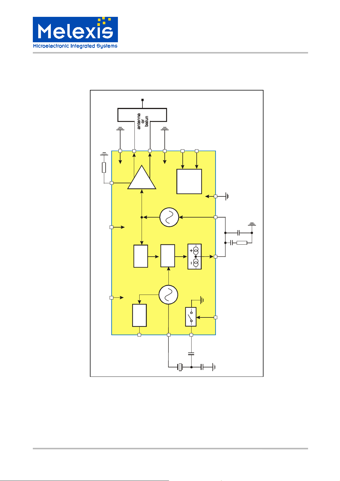
As depicted in Fig.1, the TH7108 transmitter
consists of a fully integrated voltage-controlled
oscillator (VCO), a divide-by-32 divider (div32), a
phase-frequency detector (PFD) and a charge
pump. An external loop filter at pin LF determines
the dynamic behavior of the PLL and suppresses
reference spurious signals.
The VCO’s output signal fee ds the power amplifier
(PA). RF signal power P
steps from P
= –15 dBm to +1 dBm either by
o
changing the value of resistor R
voltage V
at pin PS. The open-collector differential
PS
output (OUT1, OUT 2) can be used to eit her directl y
drive a loop antenna or to be converted t o a singleended impedance by means of a balanced-tounbalanced (balun) transformer. For maximum
available output power, the differential output
should be matched to a load of approx. 1 kΩ.
Bandgap biasing ensures stab le operation of the IC
at a power supply range of 2.2 V to 5.5 V.
FSK Modulation
A Colpitts crystal oscillator (XOSC) is used as the
reference oscillator of a phase-locked loop (PLL)
synthesizer. FSK m odulation is achie ved by pulling
the crystal (XTAL) through the data. So a CMOScompatible data stream applied at input DATA
digitally modulates the XOSC. Two external pu lling
capacitors CX1 and CX2 allow the FSK deviation
and center frequenc y to be adjusted i ndependentl y.
At DATA = LOW CX2 is connected in parallel to
CX1 leading to the lo w-frequenc y component of the
FSK spectrum (f
); while at DATA = HIGH CX2 is
min
deactivated and the XOSC is set to its high
frequency, leading to f
An external reference signal can be directly ACcoupled to pin RO1. Then the TH7108 is used
without an XTAL. The reference signal has to
contain the FSK (or FM) and sets the carrier
frequency.
can be adjusted in six
o
or by varying the
PS
.
max
The transmitter's c arrier frequency f
by the frequency of the reference crystal f
is determined
c
that is
ref
used. The integrated P LL synthesizer ensur es that
each RF value, ranging fr om 800 MHz to 9 30 MHz,
can be achieved by using a cr ystal with reference
frequency accordin g to: f
= fc/N, where N = 32 is
ref
the PLL feedback divider ratio.
Frequency Modulation (FM)
For FM operation an external varactor is required. It
simply acts as a pulling capacitor connected in
series to the crystal. Then the analog modulation
signal, applied through a series resistor, directly
modulates the XOSC.
ASK Modulation
The TH7108 can be ASK-modulated by applying
data directly at pin PS. This turns the PA on and off
and therefore leads to an ASK signal at the output.
Mode Control Logic
The mode control logic allows four different m odes
of operation as listed in the following table. The
mode control pins ENCK and ENTX are pulleddown internally. This guarantees that the whole
circuit is shut down if these pins are left floating.
The clock output CKOUT can be used to drive a µC.
This output can be activated by the ENCK pin as
required for any specific application. Clock
frequency is 1/8 of the reference crystal frequency.
ENCK ENTX Mode Description
0 0 all OFF whole circuit in standby
0 1 TX only TX functionality only, no
clock available
10clock
only
11all ON
TX in standby and clock
available
TX functional and clock
available
Table 1: Modes of operation
3901007108 Page 2 of 12 Data Sheet
Rev. 005 Dec. 2001
Page 3
Block Diagram
RPS
VEE
14
OUT1
13
VCC
OUT2
12
VEE
11
ENTX
ENCK76
TH7108
868/915MHz
FSK/FM/ASK Transmitter
PA
div32
XOSC
VCC 10 VCC PS15 9
div 8
8
RO1
CKOUT
VCO
PFD
mode
control
2LF2 SUB
16
pump
charge
1
DATA LF1
3
5
XTAL
4
RO2
CX2
CX1
CF1
CF2
RF1
Fig. 1:TH7108 block diagram with external components
3901007108 Page 3 of 12 Data Sheet
Rev. 005 Dec. 2001
Page 4
TH7108
868/915MHz
FSK/FM/ASK Transmitter
Pin Definition and Descripti on
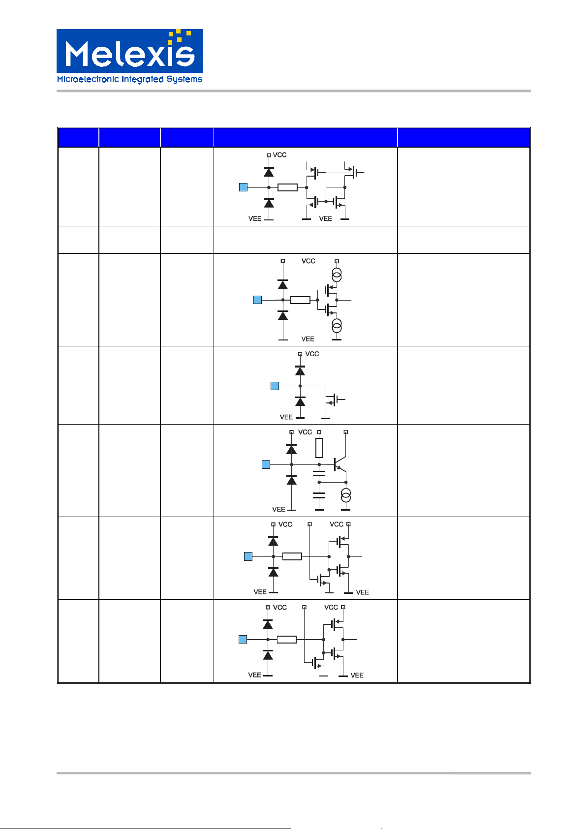
Pin No. Name I/O Type Functional Schematic Description
1 LF1 output
charge pump output,
connection to loop filter
LF1
1
200
Ω
2 SUB ground negative power supply,
substrate connection
3 DATA input
FSK data input,
CMOS-compatible
DATA
3
1.8k
4 RO2 analog I/O
XOSC FSK pulling pin,
MOS switch
RO2
4
5 RO1 analog I/O
RO1
37k
XOSC connection to XTAL,
Colpitts type crystal
oscillator
6 ENTX input
7 ENCK input
ENTX
6
ENCK
7
5
28p
28p
mode control input, CMOScompatible with internal pull-
1.1k
down
mode control input, CMOScompatible with internal pull-
1.1k
down
3901007108 Page 4 of 12 Data Sheet
Rev. 005 Dec. 2001
Page 5
TH7108
868/915MHz
FSK/FM/ASK Transmitter
Pin No. Name I/O Type Functional Schematic Description
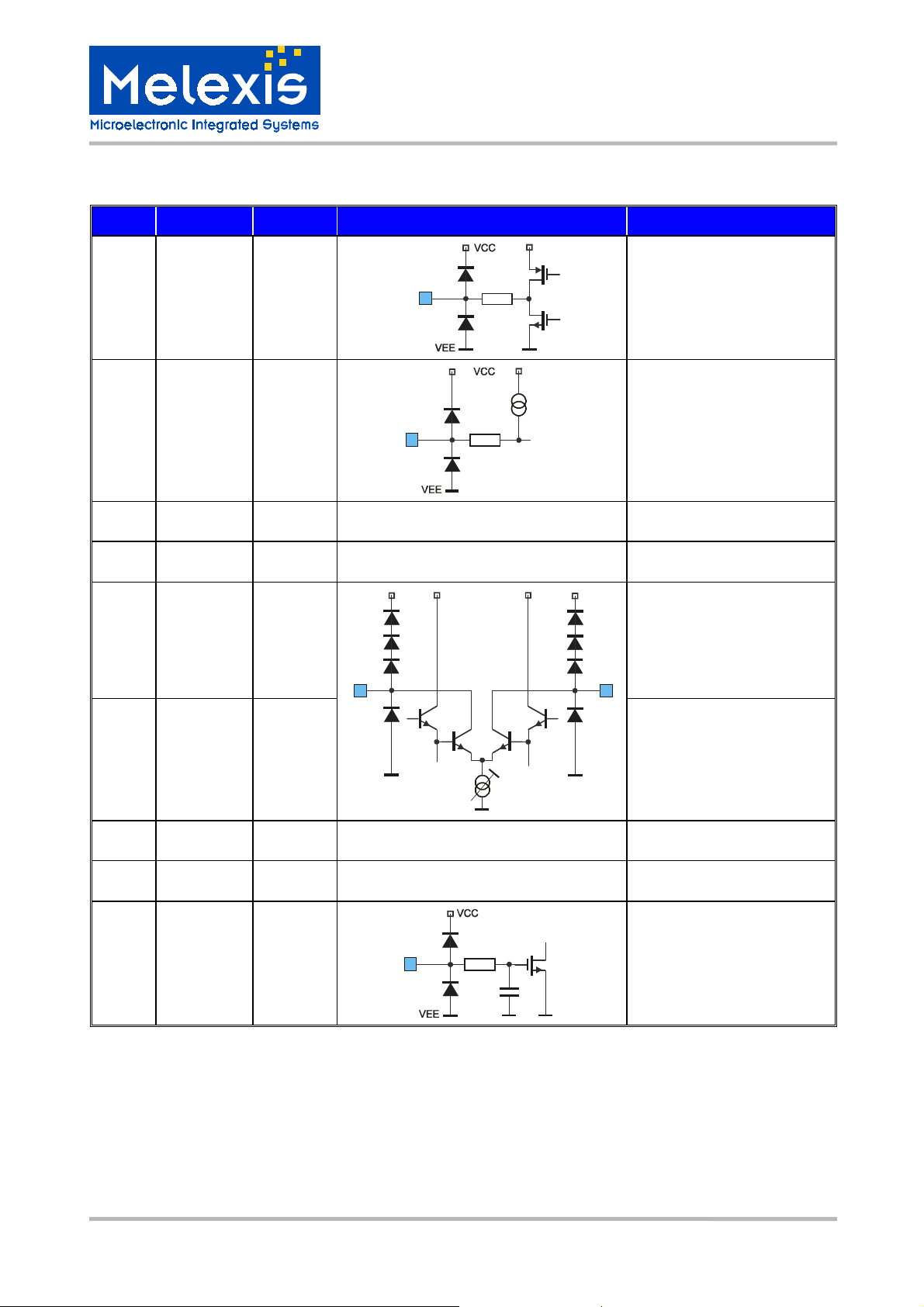
8 CKOUT output
clock output,
CMOS-compatible
CKOUT
8
200
Ω
9 PS analog I/O
power-select and ASK input,
high-impedance comparator
PS
20µA
200
Ω
9
logic
10 VCC supply positive power supply
11 VEE ground negati ve po wer supp l y
12 OUT2 output differential power amplifier
VCC
VCC
output, open collector
OUT2
OUT1
13 OUT1 output
12
13
differential power amplifier
output, open collector
VEE
VEE
VEE
14 VEE ground negati ve po wer supp l y
15 VCC supply positive power supply
16 LF2 input
VCO tuning input,
connection from loop filter
LF2
16
200
Ω
5p
3901007108 Page 5 of 12 Data Sheet
Rev. 005 Dec. 2001
Page 6
Technical Data
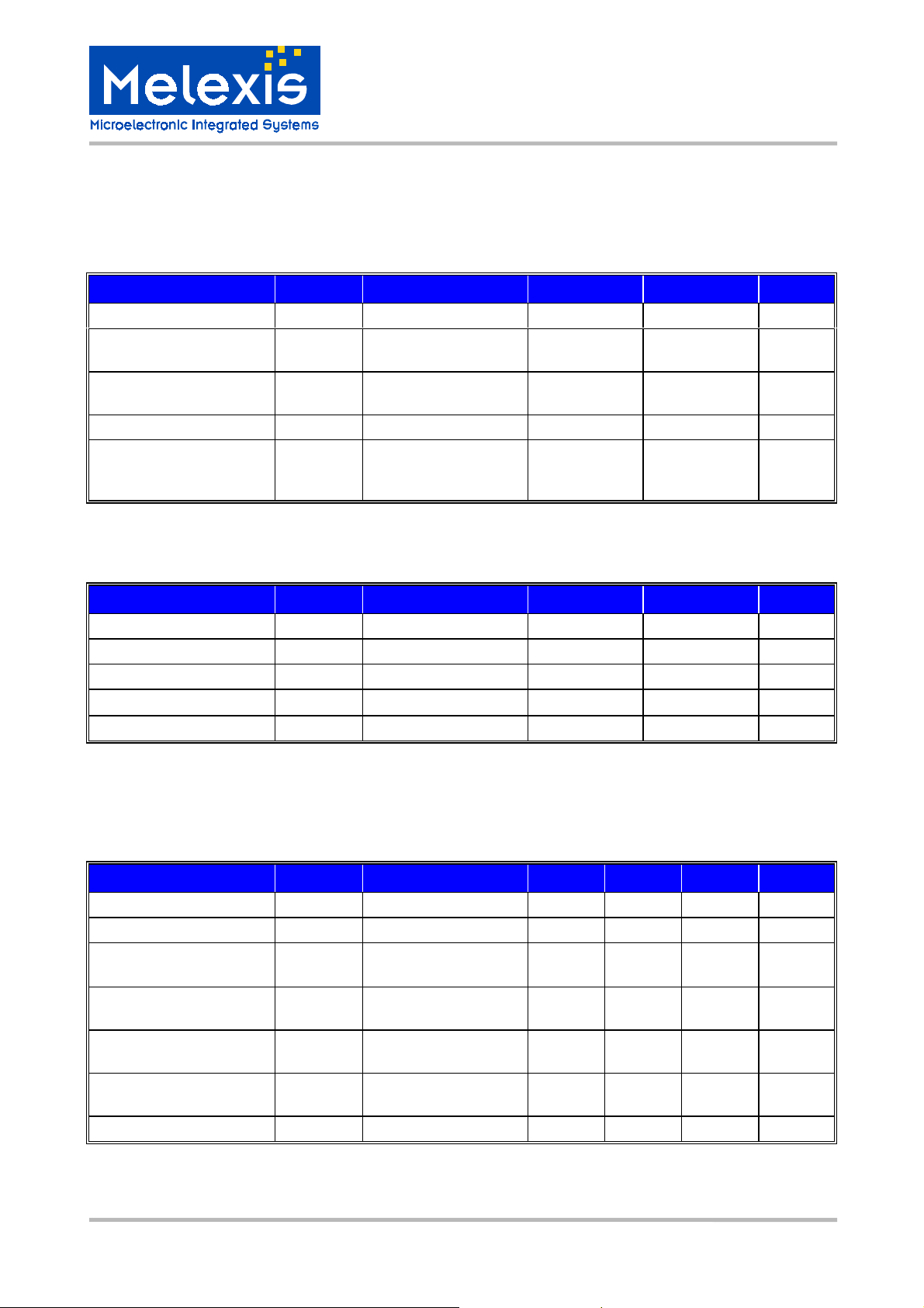
Absolute Maximum Ratings
Parameter Symbol Condition Min Max Unit
TH7108
868/915MHz
FSK/FM/ASK Transmitter
Supply voltage V
Input voltage V
Input current I
Storage temperature T
Electrostatic discharge V
Normal Operating Conditions
Parameter Symbol Condition Min Max Unit
Supply voltage V
Operating temperature T
XOSC frequency f
VCO frequency f
Clock frequency f
cc
in
in
STG
ESD
cc
a
ref
c
clk
-0.3 7.0 V
DATA, ENCK, ENTX
-0.3 VCC+0.3 V
pins
DATA, ENCK, ENTX
-1.0 1.0 mA
pins
-40 150 °C
human body model,
-1.0 +1.0 kV
MIL STD 833D
method 3015.7
2.2 5.5 V
-40 85 °C
set by the crystal 25 29 MHz
fc = 32 • f
f
= f
/ 4 3.12 3.62 MHz
clk
ref
ref
800 930 MHz
DC Characteristics
all parameters under normal operating conditions, unless otherwise stated;
typical values at T
= 23 °C and Vcc = 3 V
a
Parameter Symbol Condition Min Typ Max Unit
Standby current I
Clock only current I
Operating current I
SBY
clk
cc
ENCK=0, ENTX=0 0.05 0.1 µA
ENCK=1, ENTX=0 0.7 0.9 1.1 mA
ENCK=x, ENTX=1,
81011mA
RPS=56kΩ
Input HIGH voltage V
HIGH
DATA, ENCK, ENTX
0.7*V
cc
Vcc+0.3 V
pins
Input LOW voltage V
LOW
DATA, ENCK, ENTX
-0.3 0.3*V
cc
V
pins
Input current I
in
DATA=x, ENCK=0,
-1 1 µA
ENTX=0
Pull down current I
pd
ENCK=1, ENTX=1 2 8 15 µA
3901007108 Page 6 of 12 Data Sheet
Rev. 005 Dec. 2001
Page 7
FSK/FM/ASK Transmitter
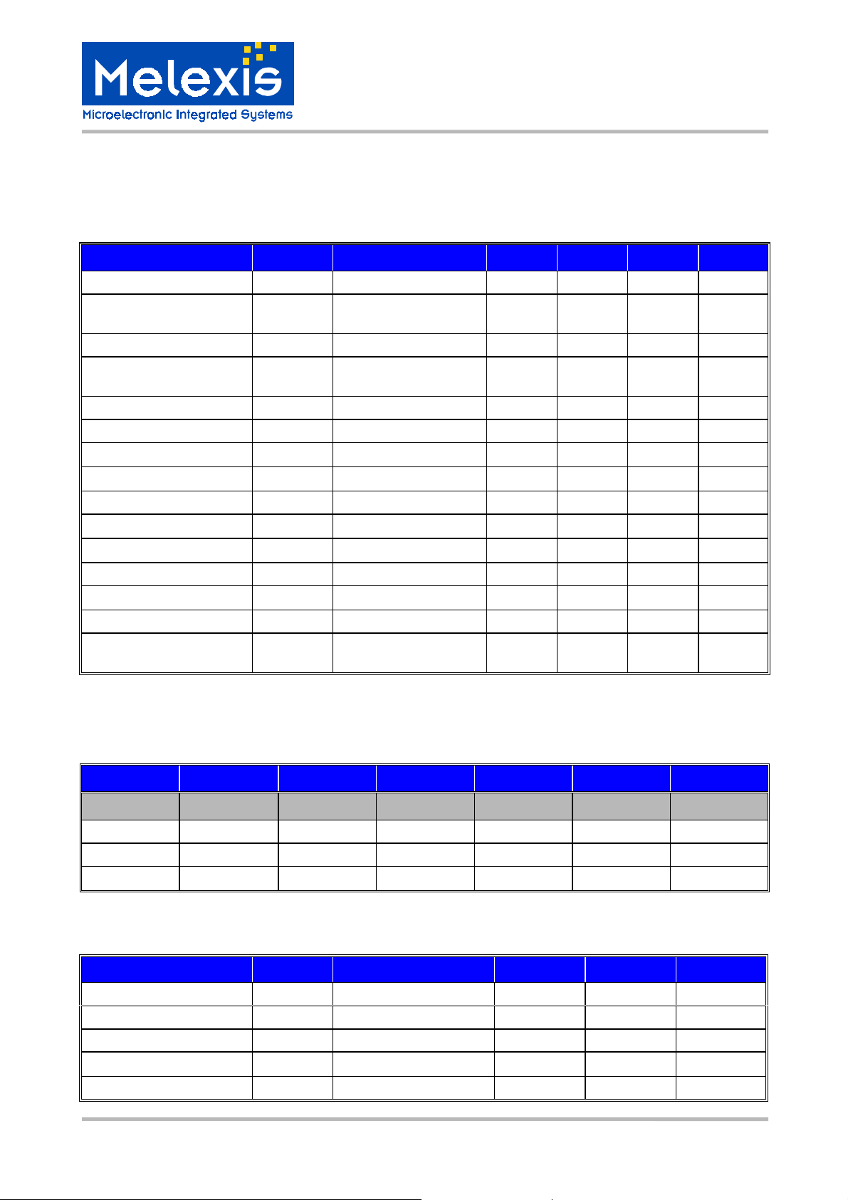
AC Characteristics
all parameters under normal operating conditions, unless otherwise stated;
typical values at T
ENCK = 1, ENTX = 1, RPS = 56 kΩ, f
Parameter Symbol Condition Min Typ Max Unit
= 23 °C and Vcc = 3 V;
a
c
= 868.3 MHz, test circuit shown in Fig. 2
TH7108
868/915MHz
Output power P
FSK deviation
Data rate FSK R
FM deviation
Modulation frequency FM f
Data rate ASK R
∆f
FSK
FSK
∆f
mod
ASK
Reference spurs P
Clock spurs P
Harmonic content P
harm
Spurious output signal P
Phase noise PN
VCO gain K
Charge pump current I
Clock voltage swing V
Start-up time t
VCO
CP
CKOUT
on
clk
FM
ref
off
o
depends on CX1, CX2
±5 ±30 ±100
-1 dBm
kHz
and crystal parameter
NRZ 20 kbit/s
adjustable with
varactor and V
±6
FM
kHz
5kHz
NRZ 40 kbit/s
@ fc ± f
@ fc ± f
ref
clk
@ 2fc , 3fc , 4f
≤ 0.1V
V
PS
± 500kHz
@ f
c
c
-44 dBm
-44 dBm
-40 dBm
-60 dBm
-87 dBc/Hz
300 MHz/V
±260
C
= 5pF 2 V
load
from ”all OFF” to any
0.9 ms
µA
pp
other mode
Output Power Selection
typical values at T
ENCK = 1, ENTX = 1, f
RPS / kΩΩΩΩ
VPS/ V
= 23 °C and Vcc = 3 V:
a
= 868.3 MHz, test circuit shown in Fig. 2
c
≥≥≥≥ 68
≥≥≥≥ 2
56 47 39 27 15
1.2 0.9 0.7 0.5 0.3
Icc / mA 12.5 9.5 8.5 7.8 7.0 6.2
Po / dBm 1 -2 -5 -8 -10 -15
P
harm
/ dBm
≤-40 ≤-40 ≤-40 ≤-45 ≤-45 ≤-50
Crystal Parameter
Parameter Symbol Condition Min Max Unit
Crystal frequency f
crystal
Load capacitance C
Static capacitance C
Resonance resistance R
Spurious response a
load
0
m
spur
fundamental mode, AT 25 29 MHz
10 15 pF
7pF
40
-10 dB
Ω
3901007108 Page 7 of 12 Data Sheet
Rev. 005 Dec. 2001
Page 8
TH7108
868/915MHz
FSK/FM/ASK Transmitter
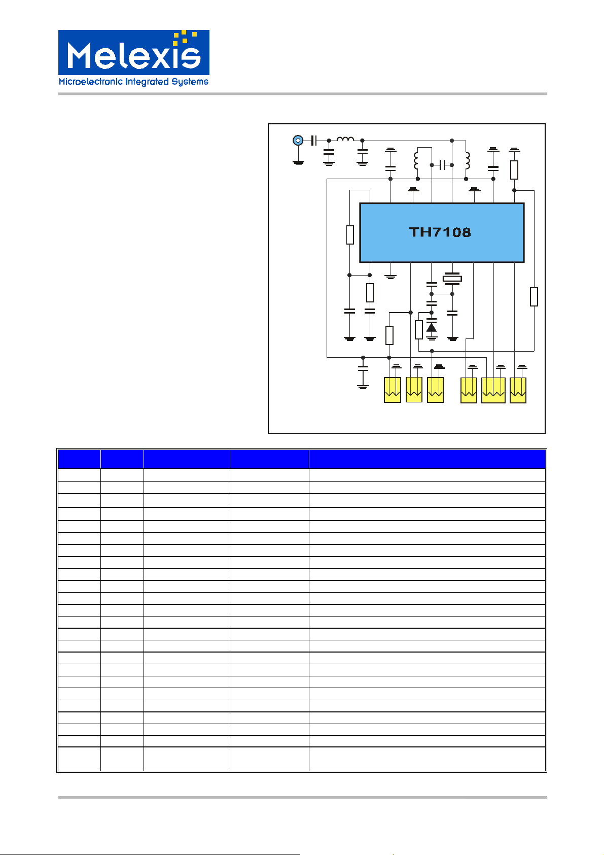
Test Circuit
Fig. 2: Test circuit for FSK, ASK and FM;
with 50Ω matching network
Test circuit component list to Fig. 2
OUT
C4
C3
RF2
CF2
L3
C7
C2
16
LF1
1
CF1
LF2
RF1
C5
L1
15
VCC
SUB
2
R1
1
12
2
VCC
GND
14
DATA
3
CX2
CX3
FSK
C1
13
VEE
OUT1
RO2
4
V1
R2
1
2
GND
GND
FM/ASK
12
OUT2
RO1
5
XTAL
CX1
L2
C6
RPS
10
11
VEE
ENTX
6
GND
ENTX
9
PS
VCC
ENCK
CKOUT
7
8
R3
1
3
21212
GND
GND
VCC
ENCK
CKOUT
Part Size Value Tolerance Description
CF1 0603 5.6 nF
CF2 0603 NIP
CX1
CX1
_FSK
_ASK
0603 56 pF
0603 18 pF
CX2 0603 1 nF
CX3 0603 1 nF
C1 0603 0.47 pF
C2 0805 1.0 pF
C3 0805 1.8 pF
C4 0603 150 pF
C5 0603 330 pF
C6 0603 330 pF
C7 1206 220 nF
L1 0603 10 nH
L2 0603 15 nH
L3 0805 15 nH
RF1 0805
RF2 0805
RPS 0805
R1 0805
R2 0805
1.6 kΩ±10%
2.0 kΩ±10%
56 kΩ±10%
470 kΩ±10%
30 kΩ±10%
R3 0805
0 Ω±10%
±10%
±10%
±5%
±5%
±5%
±10%
±5%
±5%
±5%
±5%
±10%
±10%
±20%
±5%
±5%
±5%
V1 SOD323 BB535 varactor diode (for FM only)
XTAL HC49/S
27.1344 MHz
fundamental wave
±30ppm calibr.
±30ppm temp.
loop filter capacitor
loop filter capacitor
XOSC capacitor for FSK (∆f = ±30 kHz)
XOSC capacitor for ASK, trimmed to f
XOSC capacitor (for FSK only)
XOSC capacitor (for FM only)
impedance matching capacit o r
impedance matching capacit o r
impedance matching capacit o r
impedance matching capacit o r
blocking capacitor
blocking capacitor
blocking capacitor
impedance matching inductor
impedance matching inductor
impedance matching inductor
loop filter resistor
loop filter resistor
power-select resistor
optional pull-up resistor
varactor bias resistor, (for FM only)
ASK jumper, (for ASK only)
crystal, C
R
m, max
= 12 pF to 15 pF, C
load
= 40 Ω
0, max
C
= 7 pF,
3901007108 Page 8 of 12 Data Sheet
Rev. 005 Dec. 2001
Page 9
FSK/FM/ASK Transmitter
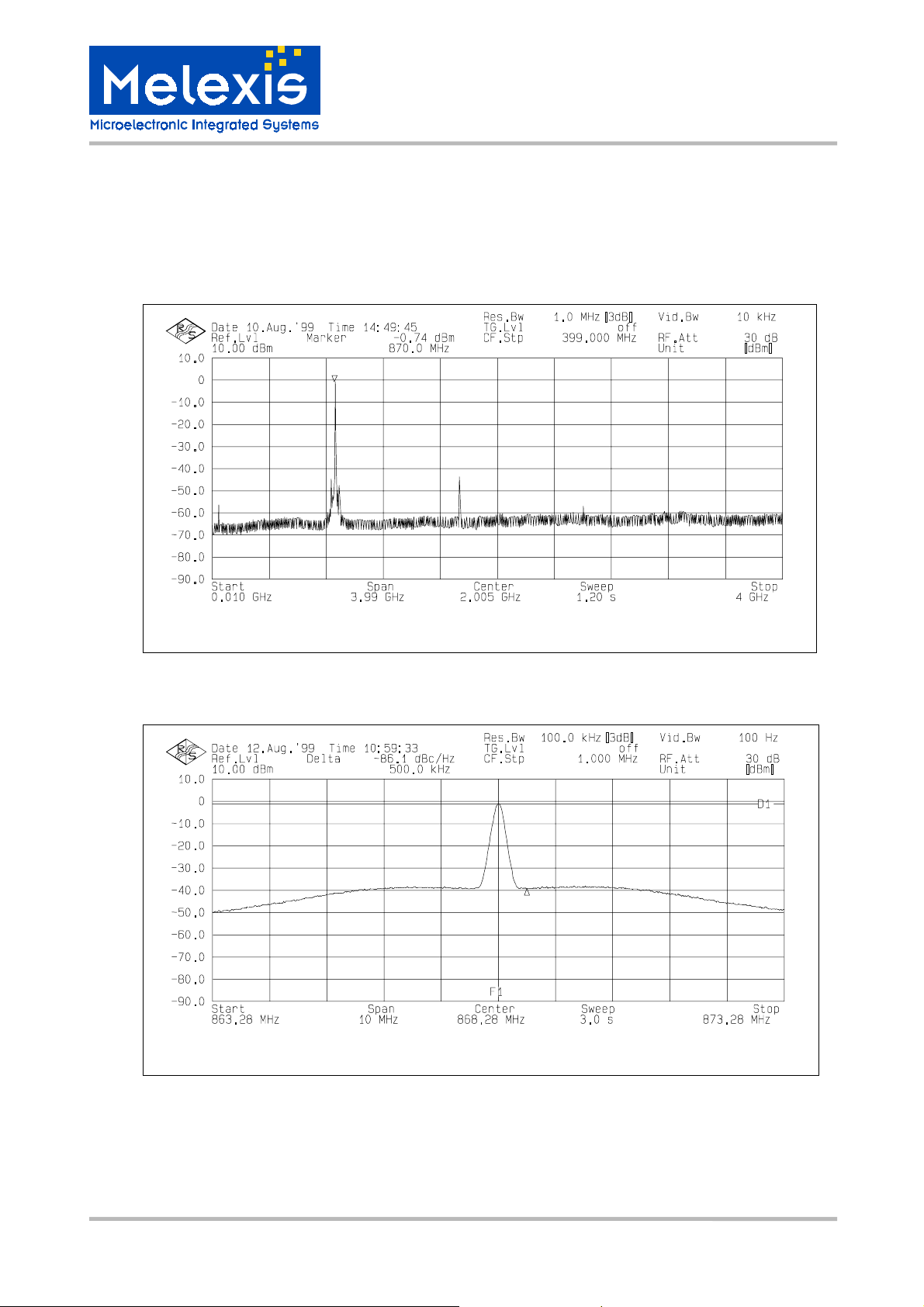
Spectrum Plots
All plots depict TH7108‘s typical performance at Vcc = 3.0 V and Ta = 23 °C,
derived with the test circuit shown in Fig. 4.
Fig. 3: RF output signal and spurious emissions, CW mode (DATA = HIGH)
TH7108
868/915MHz
Fig. 4: Single-sideband phase noise at 500 kHz offset, CW mode (DATA = HIGH)
3901007108 Page 9 of 12 Data Sheet
Rev. 005 Dec. 2001
Page 10
TH7108
868/915MHz
FSK/FM/ASK Transmitter
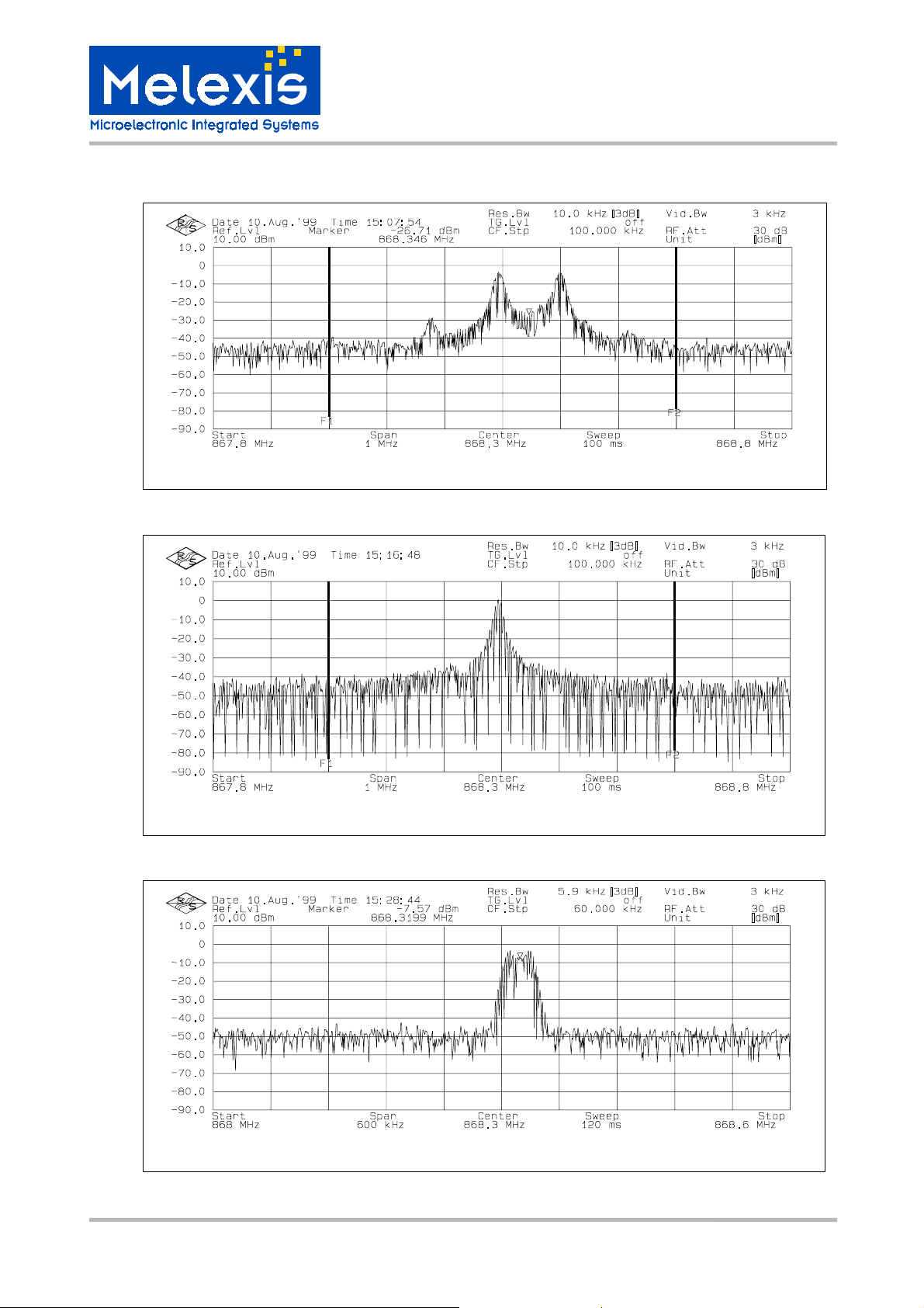
Fig. 5: FSK modulation with R
Fig. 6: ASK modulation with R
= 7.6 kbit/s NRZ, SRD band from 868.0 to 868.6 MHz indicated
FSK
= 4 kbit/s NRZ, SRD band from 868.0 to 868.6 MHz indicated
ASK
Fig. 7: FM with f
3901007108 Page 10 of 12 Data Sheet
Rev. 005 Dec. 2001
= 2 kHz, FM input signal with 1 Vpp around 1.5 V
mod
DC
Page 11
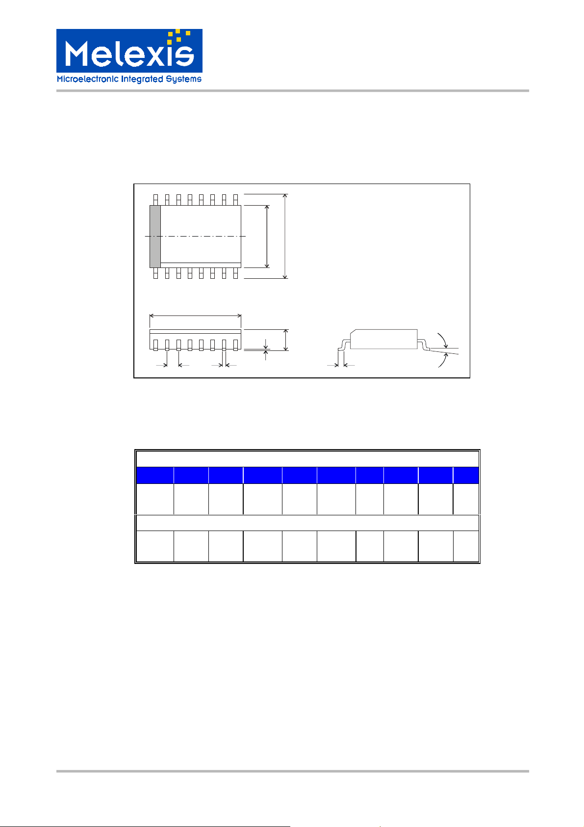
Package Information
123
TH7108
868/915MHz
FSK/FM/ASK Transmitter
E1 E
D
A1 A
e
all Dimension in mm, coplanarity < 0.1mm
D E1 E A A1 e b L
min 9.80 3.81 5.80 1.32 0.10 1.27 0.36 0.41 0°
max 9.98 3.99 6.20 1.72 0.25 0.46 1.27 8°
all Dimension in inch, coplanarity < 0.004”
min 0.386 0.150 0.2284 0.060 0.0040 0.05 0.014 0.016 0°
max 0.393 0.157 0.2440 0.068 0.0098 0.018 0.050 8°
b
Fig. 8: SOIC16 (Small Outline Package)
L
α
αααα
3901007108 Page 11 of 12 Data Sheet
Rev. 005 Dec. 2001
Page 12

Your Notes
TH7108
868/915MHz
FSK/FM/ASK Transmitter
Important Notice
Devices sold by Mele xis are covered by th e warranty and pate nt indemnification pr ovisions appearing in i ts Term of S ale. Melexis makes no warrant y,
express, statutory, implied, or by description regarding the informatio n set forth herein or re garding the freedom of the described devices from patent
infringement. Melexis res erves the ri ght to cha nge sp ecific ations and p rices at any time a nd without notice . Theref ore, p rio r to designing this product into a
system, it is necessary t o check with Melexis for curr ent information. This product is intended for use in norm al commercial applications. Applications
requiring extended temperature range, unusual environmental requirements, or high reli ability applications, such as military, medical life-support or lifesustaining equipment are specifically not recommended without additional processing by Melexis for each application.
The information furnis hed by Melexis is believed to be cor rect and accurate. How ever, Melexis shall not be liable to recipi ent or any third party for any
damages, including b ut not limited to personal injury, pro perty damage, loss of p rofits, loss of use , interrupt of business or indirect, speci al incidental or
consequential dama ges, of any kind, in connection wit h or arising out of the fu rnishing, per formance or u se of the techni cal data herei n. No obligati on or
liability to recipient or any third party shall arise or flow out of Melexis’ rendering of technical or other services.
© 2000 Melexis NV. All rights reserved.
For the latest version of this document. Go to our website at
www.melexis.com
Or for additional information contact Melexis Direct:
Europe and Japan: All other locations:
Phone: +32 1361 1631 Phone: +1 603 223 2362
QS9000, VDA6.1 and ISO14001 Cer tif ied
3901007108 Page 12 of 12 Data Sheet
Rev. 005 Dec. 2001
 Loading...