

Page 1
TH3122
K-Bus Transceiver with integrated Voltage Regulator
Features and Benefits
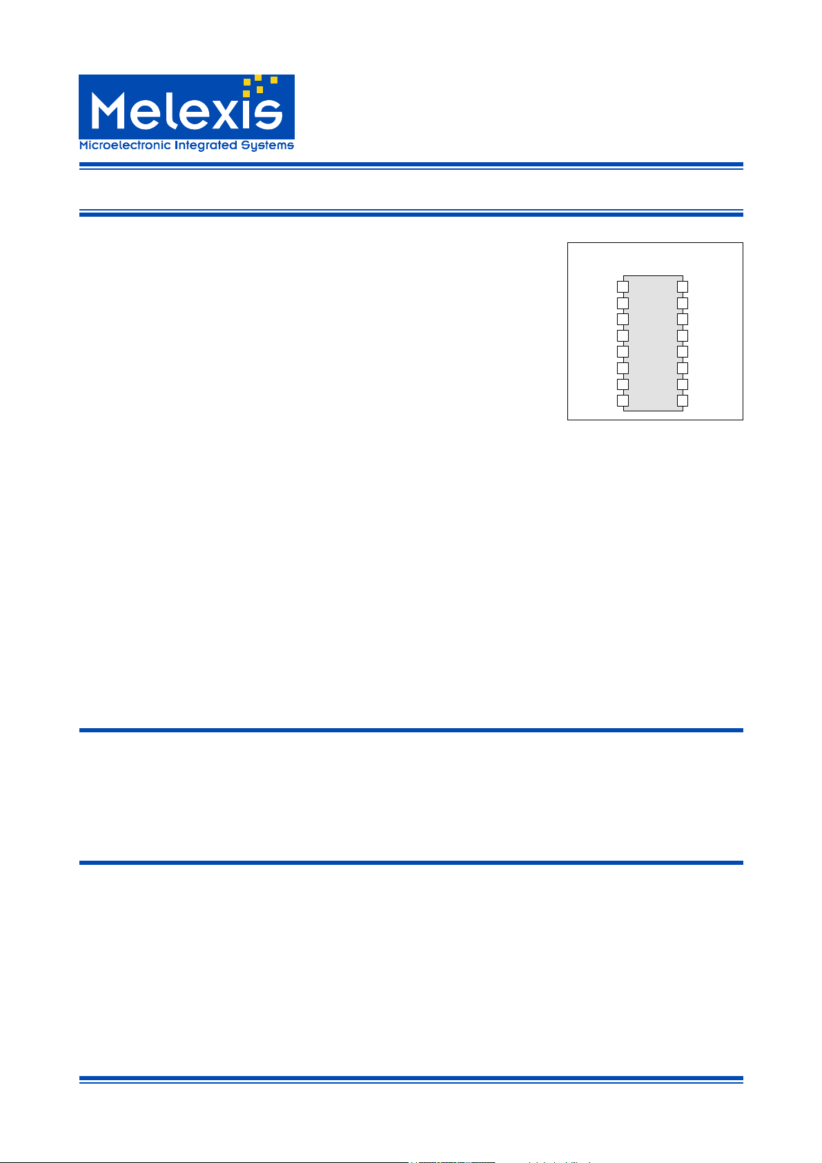
Pin Diagram
SOIC16
K-Bus Transceiver:
PNP-open emitter driver with slew rate control and current limitation
BUS input voltage -24V ... 30V (independently of V
)
S
ISO 9141 and ODBII compliant
Possibility of BUS wake up
Operating voltage V
= 5.5 ... 16 V
S
Very low standby current consumption <100 µA
in normal mode (< 50 µA in sleep mode)
Linear low drop voltage regulator:
Output voltage 5V± 2%
Output current max. 100mA
Output current limitation
Overtemperature shutdown
Configurable reset time (15ms/100ms) and reset threshold voltage (3.15V / 4.65V)
Low voltage detection at VS
Wake-up by K-BUS traffic and start-up capable independent of EN voltage level
VS VCC
EN SENSE
VTR
GND
GND
BUS
SI
SO
1
2
3
4
5
6
7
TH3122
16
15
14
13
12
11
10
98
RESET
GND
GND
TxD
RxD
SEN/STA
Universal comparator with an input voltage range –24V … 30V
and digital output
Load dump protected (40V)
Ordering Information
Part No. Temperature Range Package
TH3122 -40ºC...125ºC SOIC16, 300mil
General Description
The TH3122 consists a low drop voltage regulator
5V/100mA and a K-Bus transceiver. The transceiver is suitable for K-Bus systems conform to
ISO 9141.
The combination of voltage regulator and bus
transceiver in combination with the monitoring
functions make it possible to develop simple, but
powerful and cheap nodes in K-Bus systems.
The wide output current area and the configurable
reset time and reset voltage works together with
many different microcontrollers.
www.melexis.com Page 1 Datasheet Rev 1.0 July 2001
Page 2
Functional Diagram
TH3122
K-Bus Transceiver with integrated Voltage Regulator
VS
EN
VTR
BUS
7.8V
+5V
6.8V
V
thH
V
thL
pnp Control
slew
rate
foldback
Power Supply
Reset-Logic
VTR-Logic
OSC
Wake-up
Bus-Logic
VCC
Over Temp
SENSE
+5V
RESET
RxD
TxD
SEN/STA
+5V
SI
V
THSI_H
V
THSI_L
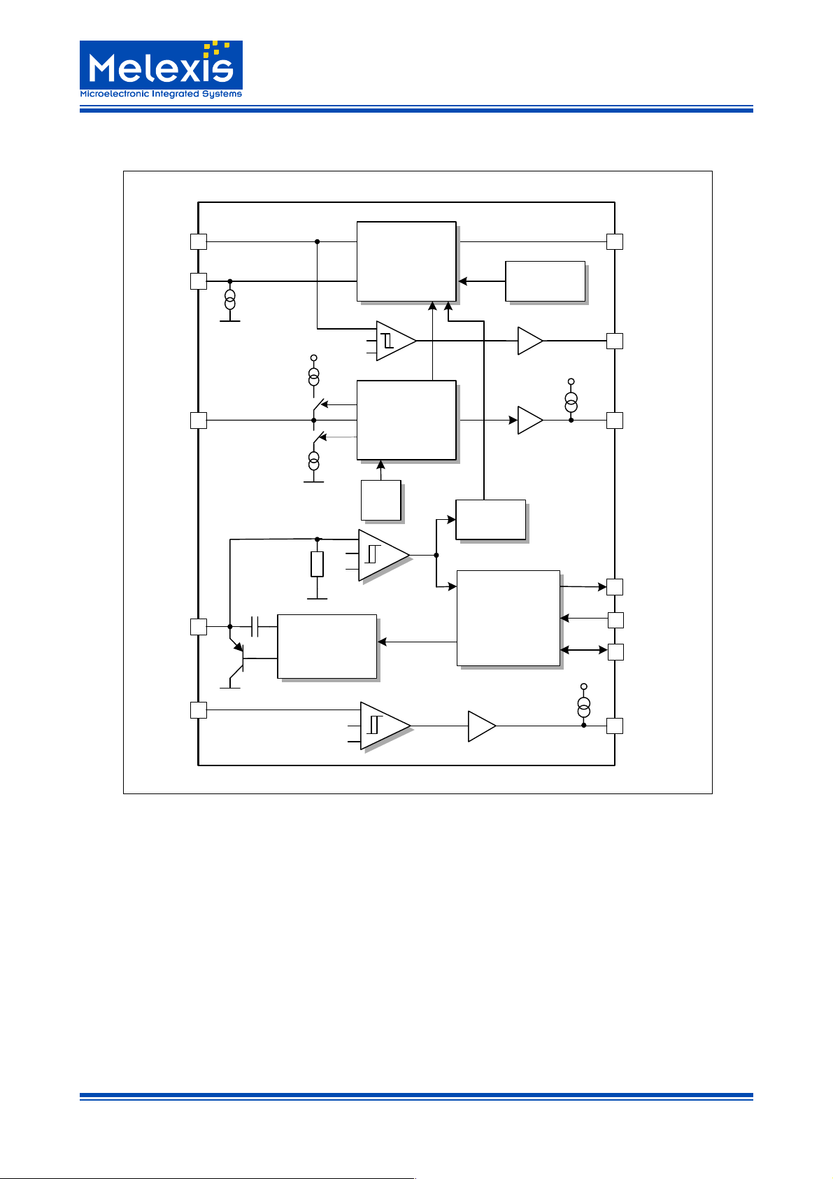
Figure 1 - Block Diagram
SO
www.melexis.com Page 2 Datasheet Rev 1.0 July 2001
Page 3
K-Bus Transceiver with integrated Voltage Regulator
Functional Description
The TH3122 consists a voltage regulator 5V/100mA and
a K-Bus transceiver, which is a bi-directional bus interface device for data transfer between K-Bus and the KBus protocol controller.
TH3122
Also integrated into the transceiver are a voltage and
time controlled reset management, power down, wake
up function and a universal comparator for extended applications.
to Wake-up
Logic
RxD
Control-
logic
POR
TxD
SENSE
ESD
ESD
VCC
VCC
VBAT
POR
VCC
Bit-Compare
Constant-Low
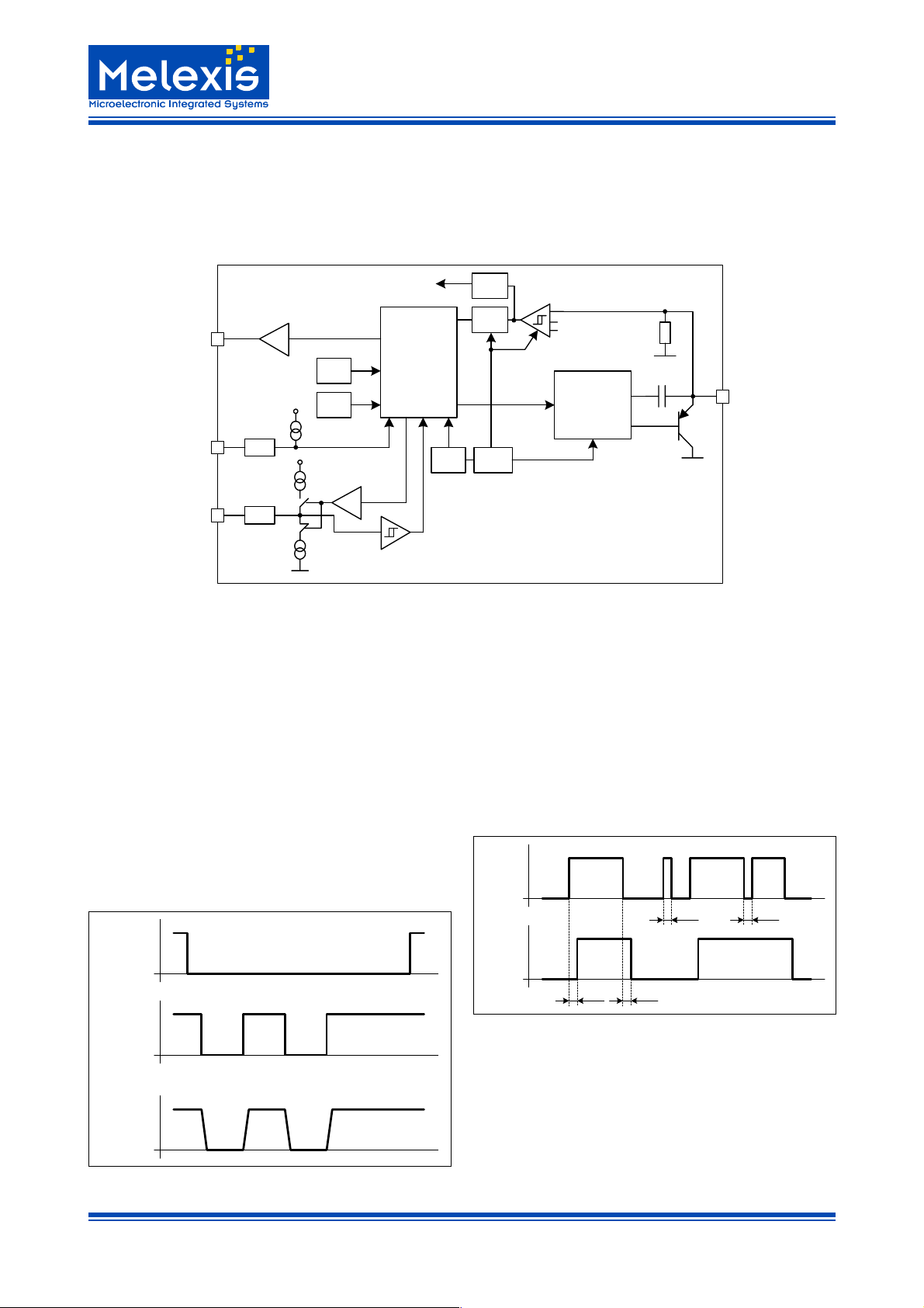
Figure 2 - Block Diagram K-Bus Transceiver
K-BUS Interface
The BUS Interface builds the connection between the serial 5V bus line of the protocol controller and the 12V KBus line.
The transceiver consists a pnp-driver with slew rate control and fold-back characteristic and consists as well in
the receiver a high voltage comparator followed by a debouncing unit.
Transmit Mode
During the transmission the data at the pin TxD will be
transferred to the pin BUS. To minimize the electromag-
SEN/STA
t
debWake
OSC
t
debBUS
Vref
Biasing
V
thH
V
thL
pnp Control
- slew rate
- I
B
- foldback
BUS
netic emission of the bus line, the TH3122 has an integrated slew rate control.
Receive Mode
The data at the pin BUS will be transferred to the pin
RxD. Short spikes on the bus signal are suppressed by
the implemented debouncing circuit.
BUS
< t
debH
RxD
< t
debL
TxD
BUS
Figure 3 - Transmit Mode Pulse Diagram
t
debH
t
debL
Figure 4 - Receive Mode Pulse Diagram
www.melexis.com Page 3 Datasheet Rev 1.0 July 2001
Page 4
TH3122
K-Bus Transceiver with integrated Voltage Regulator
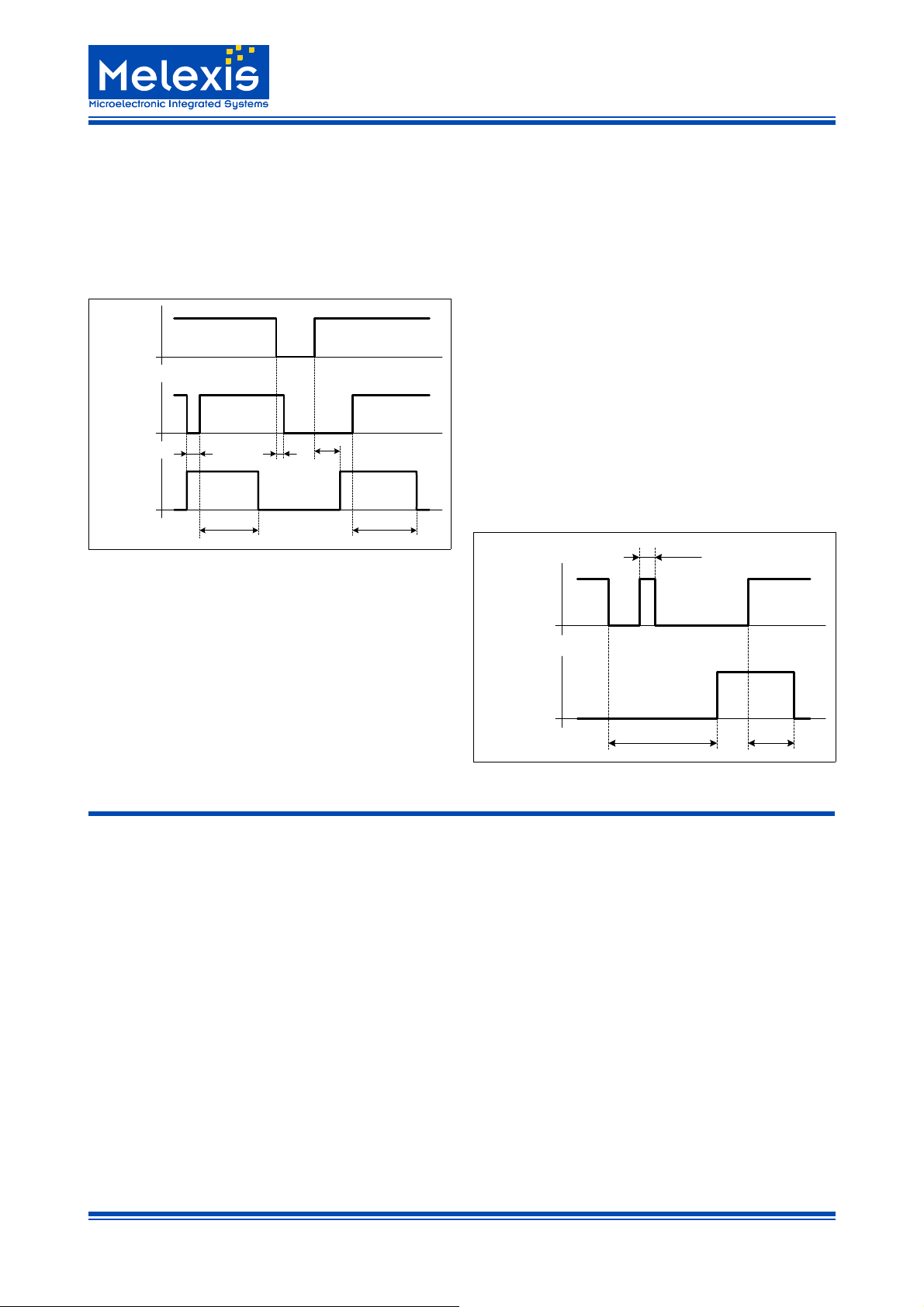
Bit Compare
Are the signals at the pin TxD and the pin BUS
within a specified time t
not identical, the
bc
transmission will be interrupted.
If both signals at TxD and BUS are “High” within
the time t
the transmission will be enabled. The
ena
bit-compare-function is activ when the pin SEN/
STA is open (not overwritten).
BUS
RxD
t
t < t
bc
SEN/STA
t
ena
Figure 5 - Bit Compare Pulse Diagram
bc
t
ena
Using this pin as an input the transmission path
can be overwritten (independent of bit-compare
and constant-low function):
SEN/STA=”0”
forcing the transmission path free
SEN/STA=”1”
disable the transmission path
Constant Low Switch Off
A falling edge at pin TxD (from “1” to “0”) starts the
internal constant low timer (SEN/STA open).
If the low level “0” is valid for the time t
low
the
transmission unit of the TH3122 will be disabled.
The receive unit is still active. A high level “1” at
TxD with a minimum pulse width of t
reset the
rec
constant low timer.
Transmitting is possible not until TxD and BUS is
High for the time t
ena
.
t < t
rec
SEN/STA
The pin SEN/STA is bidirectional. Used as an
output the pin indicates whether the transmit-path
is enabled or disabled:
SEN/STA =”0”
transmission path is enabled
SEN/STA =”1”
transmission path is disabled
Linear Regulator and Controlling Functions
Regulator
The TH3122 has an integrated linear regulator with an
output voltage of 5V ±2% and an output current of max.
100mA. The regulator is switched on or off with a signal
on the EN pin or wake up with a BUS signal.
Initialization
The initialization is started if the power supply is switched
on, or after the temperature limitation has switched off
the regulator or in case of BUS traffic (wake up).
If the V
time t
voltage level is higher than V
CC
is started. This reset time is determined by the
RES
RESEIN
, the reset
TxD
SEN/STA
t
low
t
ena
Figure 6 - Constant Low Pulse Diagram
voltage level on the VTR pin (see table VTR Programming). After t
a rising edge on the RESET output is
RES
generated (see figure 7 - Initialization).
The regulator is active and can only switched off with a
falling edge on EN. The regulator remain with EN=high in
active mode and therefore also the V
voltage is active.
CC
The input EN has an internal pull down resistor. If
EN=high, the internal pull down current is switched off to
minimize the quiescent current.
www.melexis.com Page 4 Datasheet Rev 1.0 July 2001
Page 5
TH3122
K-Bus Transceiver with integrated Voltage Regulator
VS
V
VCC
RESET
RESEIN
t
Res
V
RES1/2
t
rr
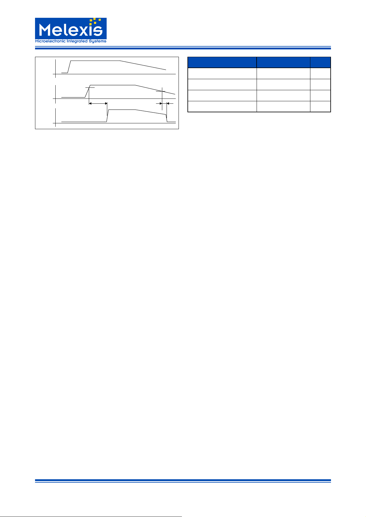
Figure 7 - Initialization
RESET Output
The RESET output is switched from low to high if VS is
switched on and VCC>V
If the voltage VCC drop below V
after the time t
RESEIN
RES1
or V
RES.
then the RESET
RES2
output is switched from high to low after the time trr has been
reached.
The voltage level for V
sponding times t
can be programmed via the ana-
RES
RES1
and V
and the corre-
RES2
logue input VTR.
Wake up with BUS traffic
If the regulator is put in standby mode it can be wake up
with the BUS interface. Every pulse on the BUS (high
pulse or low pulse) with a pulse width of min. 45µs will
switch on the regulator.
After the BUS has wake up the regulator, it can only be
switched off with a high level followed by a low level on
the EN pin.
Reset Programming on VTR
With the VTR pin the reset switch off levels and delay
time can be programmed.
The voltage on VCC influences the reset function.
VTR-Programming
The voltage on VTR input is read out if the voltage at this
pin is higher than V
switch off voltage V
switch on the pull up current source if VTR=low or the
. This value defines the reset
RESEIN
. With the next oscillator cycle it
RES
VTR-Mode V
VTR = GND V
VTR = VCC V
VTR with R ≥ 50kΩ to GND
VTR with R ≥ 50kΩ to VCC
= V
RES
= V
RES
= V
V
RES
= V
V
RES
t
RES
= 3.15V 100ms
RES1
= 4.65V 100ms
RES2
= 3.15V 15ms
RES1
= 4.65V 15ms
RES2
Res
pull down current source if VTR=high. The sources are
active for one oscillator cycle. The level changes during
this procedures on VTR, which depends on the external
pull up or pull down resistors control the reset time t
Res
Temperature Limitation
If the junction temperature 150ºC < Tj < 170ºC the over
temperture recognition will be active and the regulator
voltage and the BUS driver will be switched off. After Tj
fall below 140ºC the TH3122 will be initialized, independently of the voltage levels on EN and BUS.
The function of the TH3122 is possible between T
Amax
and the switch off temperature, but small parameter differences can appear.
Low Voltage Detection VS
Low voltage on VS is monitored on SENSE output.
If V
has reached the level of VS =6.8V then the SENSE
S
output generates low level. The normal
operating range is VS > 7.8V and the SENSE output generates a high level.
Universal Comparator
The TH3122 consist a universal comparator for general
use. The positive input of this comparator is connected to
the pin SI. The input voltage range of SI is 0V...V
input voltage is compared with a fixed reference voltage
at high or low level and the comparator output SO drives
a 5V digital signal.
S.
The
www.melexis.com Page 5 Datasheet Rev 1.0 July 2001
Page 6
K-Bus Transceiver with integrated Voltage Regulator
Application Hints
Operating during Disturbances
The absence of VS ,VCC or GND connection or ground
shift either alone or in any combination, do not influence
or disturb the communication between other bus nodes.
Undervoltage
The reset unit secures the correct behavior of the driver
during undervoltage. The inputs have pull-up or pulldown characteristics and have therefore defined voltage
levels.
With 4.5V ≤ V
within the correct parameters .
If V
≤ VCC ≤4.5V the TxD signal is transmitted to the
RES1
bus. The receive mode is also activ.
If V
< V
CC
SENSE and SO output the correct signal if V
The specificated values of the input voltages on SO can’t
guaranteed.
≤ 5.25V the bus connection operates
CC
the bus driver is tristate.
RES1
CC
> V
RES
.
TH3122
Regulator Circuitry
The choice and dimension of the capacitor on VCC is determined by application point of view. Important parameters are the current difference on load changes and the
maximum short time voltage drop.
The VCC pin must be connected to a min. 2µF capacitor
for stable operating of the regulator in the whole operating range.
Short Circuit Proof
All in- and outputs are short circuit proof to battery and
ground. A thermal shut down circuit prevent VCC and
BUS from any damage.
Baud Rate
The TH3122 has a maximum Baud rate of 9600 Baud
(C
< 25nF, R
BUS
> 400Ω).
PU
Application Circuitry
battery reverse diode
V
Bat
100u
33uH
BUS
optional
10
100p
47n
82p
VS
EN
VTR
GND
GND
BUS
SI
SO
TH3122
SENSE
RESET
SEN/STA
VCC
GND
GND
TxD
RxD
6.8u
µµµµ
C
+5V
Port X.1
Reset
TxD
RxD
Control Unit
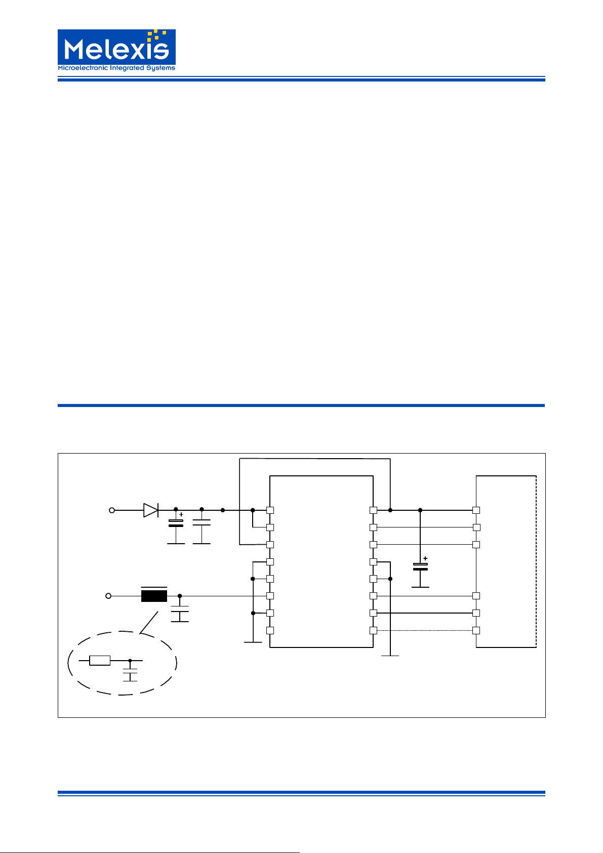
Figure 8 - Application Circuit
There should be used an LC-Filter to minimize the influence of EMI on the BUS lines.
www.melexis.com Page 6 Datasheet Rev 1.0 July 2001
Page 7
TH3122
K-Bus Transceiver with integrated Voltage Regulator
Electrical Specification
All voltages are referenced to ground (GND). Positive
currents flow into the IC. The absolute maximum ratings
given in the table below are limiting values that do not
lead to a permanent damage of the device but exceeding
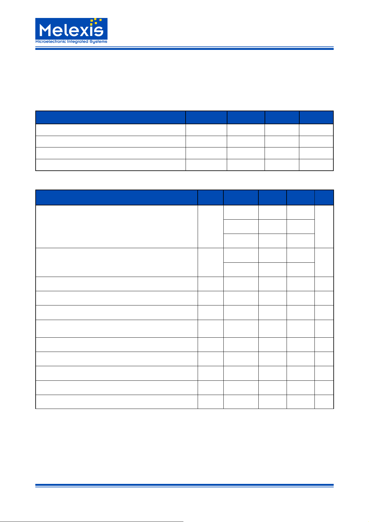
Operating Conditions
Parameter Symbol Min Max Unit
Battery voltage VS 5.25 16 V
any of these limits may do so. Long term exposure to
limiting values may affect the reliability of the device.
Reliable operation of the TH3122 is only specified within
the limits shown in ”Operating conditions”.
Supply voltage V
Operating ambient temperature T
Junction temperature
[1]
T
Absolute Maximum Ratings
Parameter
Supply voltage at VS
Input voltage at pin BUS
[2]
[2]
Difference VS-VCC V
Input voltage at pin EN and SI V
Input voltage at pin VTR, TxD, SEN/STA, SO, RESET, SENSE V
Symbol Condition Min Max Unit
V
4.75 5.25 V
CC
-40 +125 °C
A
+150 °C
J
-1.0 16
VS
≤ 1min
T
≤ 500 ms
T
- 30
V
- 40
-24 30
INBUS
T ≤ 500 ms
-0.3 40 V
S-VCC
-0.3 VS+0.3 V
INENSI
-0.3 VCC+0.3 V
IN
- 40
V
Input current at pin EN, VTR, SI, SO, SEN/STA, TxD, RxD,
RESET, SENSE
Input current for short circuit of pin VS and VCC I
Power dissipation T
= 85 °C
A
[3]
Thermal resistance from junction to ambient R
Junction temperature
[4]
Storage temperature T
-25 25 mA
I
IN
-500 500 mA
Short
P0 600 mW
50 K/W
THJA
TJ 150 °C
-55 150 °C
STG
______________________________
[1]
Junction temperature is defined in IEC 747-1
[2]
The current and voltage values are valid independent from each other.
[3]
The maximum power dissipation is defined by the ambient temperature and the thermal resistance. It can be calculated with
=(VS-VCC)*I
P
0
[4]
see over temperature protection
VCC+PBUS
. P
is the BUS driver output with normally ≤25 mW
BUS
www.melexis.com Page 7 Datasheet Rev 1.0 July 2001
Page 8
Static Characteristics
(V
= 5.25 to 16V, VCC= 4.75 to 5.25V, T
S
TH3122
K-Bus Transceiver with integrated Voltage Regulator
= -40 to +125°C, unless otherwise specified)
A
Parameter
Symbol Condition Min Typ Max Unit
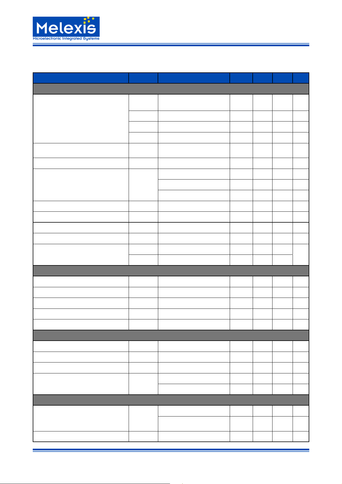
Linear Regulator
Output voltage VCC
Supply current, „normal mode“ I
I
Drop-out voltage V
Output current VCC I
Current limitation VCC I
Load capacity C
Power-on-reset threshold “VCC on” V
V
CCn
V
CCt
V
CCh
V
CCI
Snl
Ssleep
D
VCC
LVCC
load
RESEIN
5.5V ≤ VS ≤ 16V
TA = 25°C
5.5V ≤ VS ≤ 16V
V
SUP
> 16V 4.95 5.0 5.25 V
4.95 5.0 5.05 V
4.90 5.0 5.10 V
3.3 V< VS< 5.5 V VS-VD 5.1 V
= VS = 12V, Pins 8-11,
V
Supply current, „sleep mode“
EN
14-16 open
= 0V, VCC switched off 35 50
V
EN
V
≥ 4.0V, I
S
V
≥ 4.0V, I
S
V
≥ 3.3V, I
S
V
≥ 3.0V
S
= 25mA
VCC
= 100mA
VCC
= 20mA
VCC
100
200 mV
400 mV
600 mV
100 mA
VS > 0V 300 mA
ESR ≤ 5Ω
2
refered to VCC, VS > 4.6V 4.5 4.65 4.8 V
µA
µA
µF
VTR=High, VS > 0V 4.5 4.65 4.8
V
Power-on-reset threshold “V
CC
off”
RES2
V
3.0 3.15 3.3
RES1
VTR=Low, VS > 0V
SENSE-Output
VS - threshold low at SENSE V
VS - threshold high an SENSE V
Hysteresis SENSE
Output voltage low VOL I
Output voltage high V
6.8 V
SENL
7.8 V
SENH
V
100 mV
SENHYS
= 1mA 0.8 V
OUT
I
OH
= -1mA VCC-0.8 V
OUT
Enable-Input EN
Input voltage low V
Input voltage high V
Hysteresis
Pull-down current EN
I
-0.3 1.75 V
ENL
2.5 VS +0.3 V
ENH
V
100 mV
ENHYS
> V
pdEN
V
EN
V
EN
1.8 4.0 7.5
ENH
< V
70 100 130
ENL
Output RESET
I
Output voltage low VOL
= 1 mA, V
OUT
10 kΩ RESET to VCC
= VCC = 0.8 V
V
S
> 5.5 V 0.8 V
SUP
0.2 V
Pull-up current Ipu -500 -375 -250
V
µA
µA
µA
www.melexis.com Page 8 Datasheet Rev 1.0 July 2001
Page 9
K-Bus Transceiver with integrated Voltage Regulator
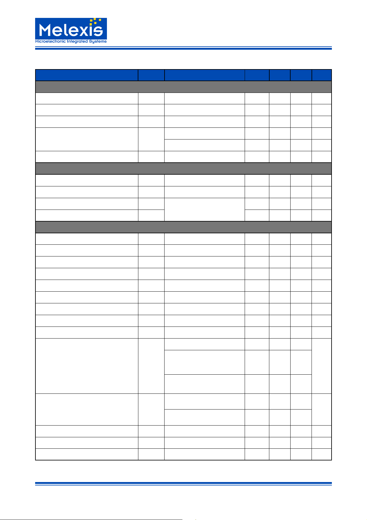
Static Characteristics (continued)
TH3122
Parameter
Symbol Condition Min Typ Max Unit
Comparator SI, SO
Threshold low SI VIL 1.05 1.16 V
Threshold High SI V
Hysteresis
1.21 1.4 V
IH
V
30 mV
HYS
= 1 mA, VS > 5.5 V 0.8 V
I
OUT
Output voltage low at SO VOL
10 kΩ SO to VCC, V
> 3.3V
CC
Pull-up current at SO Ipu -500 -375 -250
0.4 V
µA
Input VTR
Threshold low V
Threshold high V
Output current low I
Output current high I
TRL
TRH
OL
OH
V
> 3.3 V
CC
-300 -230 -160
0.15 0.25
0.75 0.85 VCC
160 230 300
VCC
µA
µA
K-Bus-Interface
Power-on-reset threshold V
Pull-up current TxD Ipu
V
POR
=V
POR
3.0 3.15 3.3 V
RES1
-500 -375 -250
µA
Pull-down current SEN/STA
Pull-up current SEN/STA
I
pdSEN
I
puSEN
Input voltage low TxD, SEN/STA V
Input voltage high TxD, SEN/STA V
Input voltage low BUS V
Input voltage high BUS V
Hysteresis BUS
V
Input restistance BUS R
Output voltage BUS
V
Current limitation BUS I
IL
IH
IL
IH
HYS
INBUS
BUS
V
LIM
250 375 500
-500 -375 -250
0.75
0 ≤ V
0 ≤ V
T
V
T
V
≤ 40 V
BUS
≤ 40 V
BUS
≤125 °C
A
= -25V
BUS
≤125 °C
A
= 12V, SENSE = low
S
0.55
50
400 600
60
0.25 VCC
0.45 VS
1500
1300
1.2
µA
µA
VCC
VS
mV
kΩ
V
V
= 12V, SENSE = low
S
> 2.5V 40
BUS
1.0
100 mA
Output voltage low RxD V
Output voltage high RxD V
I
OL
I
OH
= 1 mA
OUT
= -1mA VCC-0.8
OUT
0.8 V
www.melexis.com Page 9 Datasheet Rev 1.0 July 2001
V
Page 10
TH3122
K-Bus Transceiver with integrated Voltage Regulator
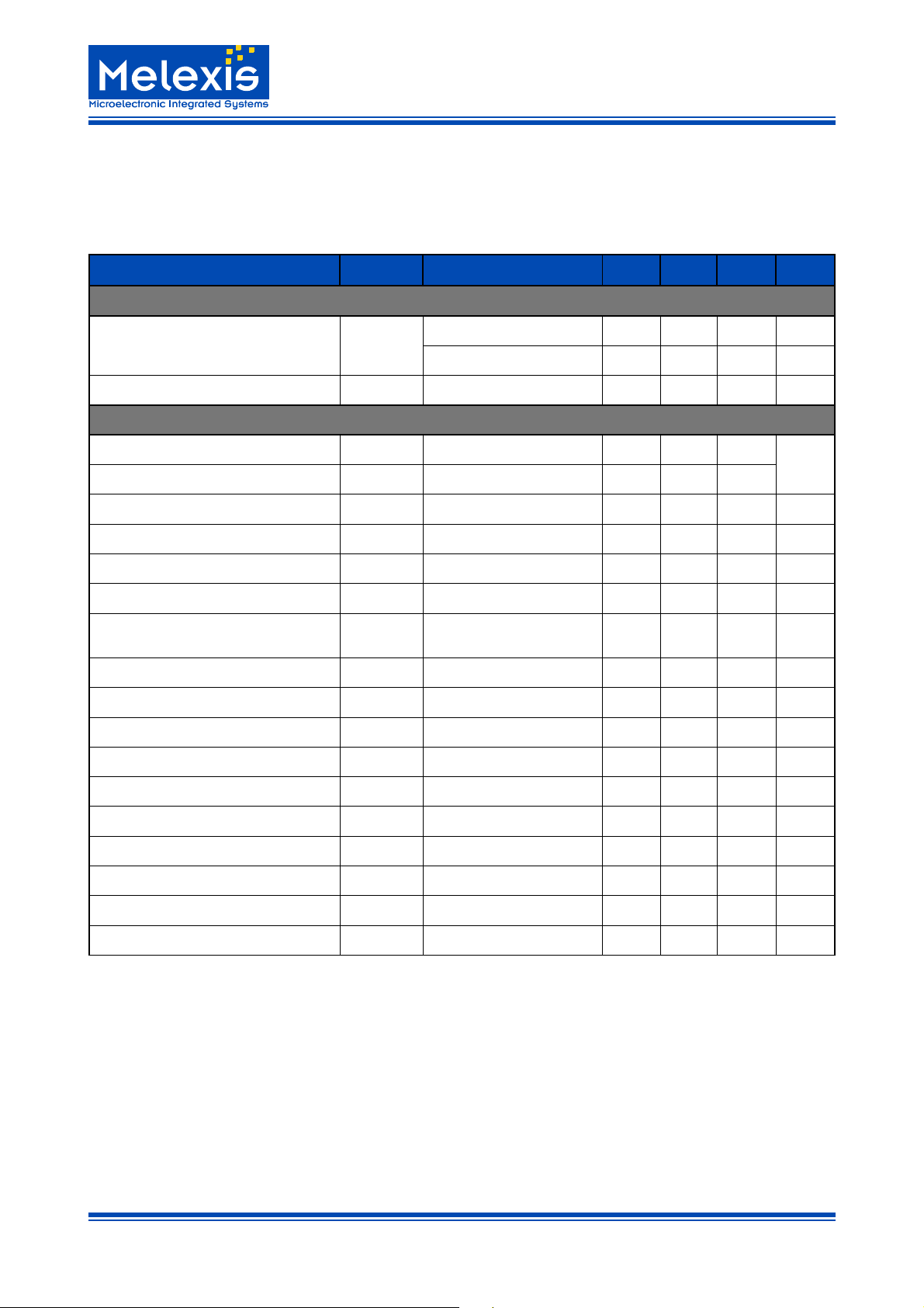
Dynamic Characteristics
All dynamic values of the table below refer to the test-schematic schown in Figure 3 - Test Circuit for Dynamic
Characteristics
For the definition of delay and transitions times see Figure 2 - TH8060 Timing Diagram.
(5.25V ≤ VS ≤ 16V, 4.75V ≤ VCC ≤ 5.25V, -40°C ≤ TA ≤ 125°C, unless otherwise specified)
Parameter
Symbol Condition Min Typ Max Unit
RESET
Reset time t
Reset rising time
K-Bus-Interface
Slew rate BUS falling edge
dV/dT
Slew rate BUS rising edge dV/d
Symmetry of Slew rate BUS dV/dT
Debouncing time BUS t
Symmetry of debouncing BUS t
debBUS
debsym
Propagation delay TxD -> RxD
Symmetry of propagation delay
TxD -> RxD
t
pdsym
Bit compare time BUS, SENSE, TxD
Recovery time BUS, TxD t
Inhibit time for transmit BUS, TxD t
Constant low switch off BUS, TxD t
R
< 1 kΩ
Res
trr
fall
Trise
sym
VTR
R
> 45 kΩ
VTR
1.0 1.6 2.2
70 100 140 ms
10 15 20 ms
3.0 6.5 10
-2.2 -1.6 -1.0
High pulse or low pulse 1.5 2.8 4.0
t
t
ena
low
rec
pd
bc
35 52 70
30 50 75
0.92 1.33 1.8 ms
3 6 12 ms
0.3
0.5
20
3.5
µs
V/µs
V/µs
µs
µs
µs
µs
µs
µs
Oscillator frequency f
Debouncing time TxD t
Debouncing time EN
Wake-up debouncing BUS t
Propagation delay SI -> SO t
Debouncing VS-SENSE t
OSC
deb
t
deb
debWake
pdcomp
deb
8 12 15 kHz
0.6 1.0 1.5
µs
200 ns
25 45 90
4 11
10 17 25
µs
µs
µs
www.melexis.com Page 10 Datasheet Rev 1.0 July 2001
Page 11
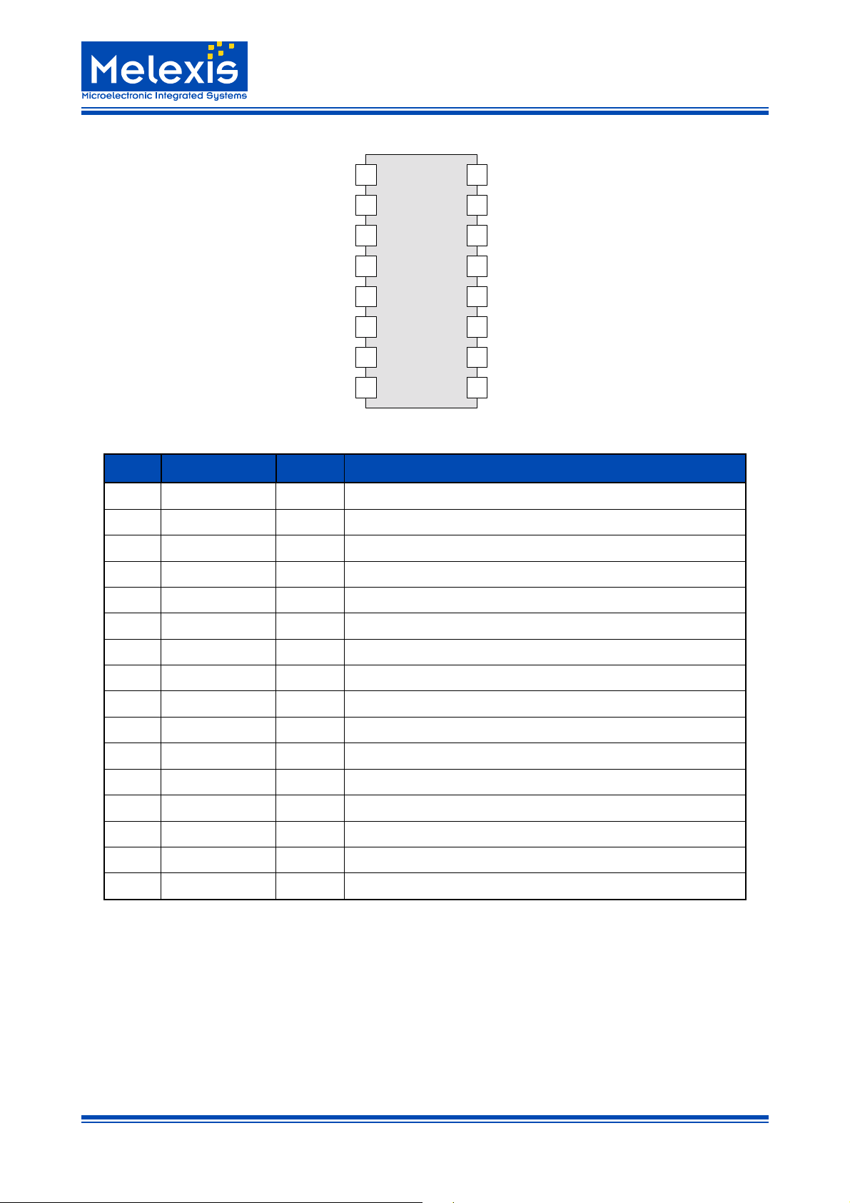
Pin Description
TH3122
K-Bus Transceiver with integrated Voltage Regulator
VS VCC
EN SENSE
VTR
GND
1
2
3
4
16
15
14
13
RESET
GND
TH3122
12
GND
11
TxD
10
RxD
98
SEN/STA
SI
5
6
7
GND
BUS
SO
Pin Name I/O Function
1 VS Supply voltage
2 EN I Enable Input voltage regulator, HV-pull-down-Input, High-active
3 VTR I Analogue Input - definition of reset time und Reset voltage level
4 GND Ground
5 GND Ground
6 BUS I/O Bi-directional bus line
7 SI I Comparator Input, HV-Input
8 SO O 5V-Comparator Output
9 SEN/STA I/O Send status
10 RxD O Receive Output, 5V-push-pull
11 TxD I 5V-Transmit Input, pull-up-Input
12 GND Ground
13 GND Ground
14 RESET O 5V-output reset, active low
15 SENSE O 5V-output of VS-Monitoring
16 VCC O Regulator output 5V/100mA
www.melexis.com Page 11 Datasheet Rev 1.0 July 2001
Page 12
K-Bus Transceiver with integrated Voltage Regulator
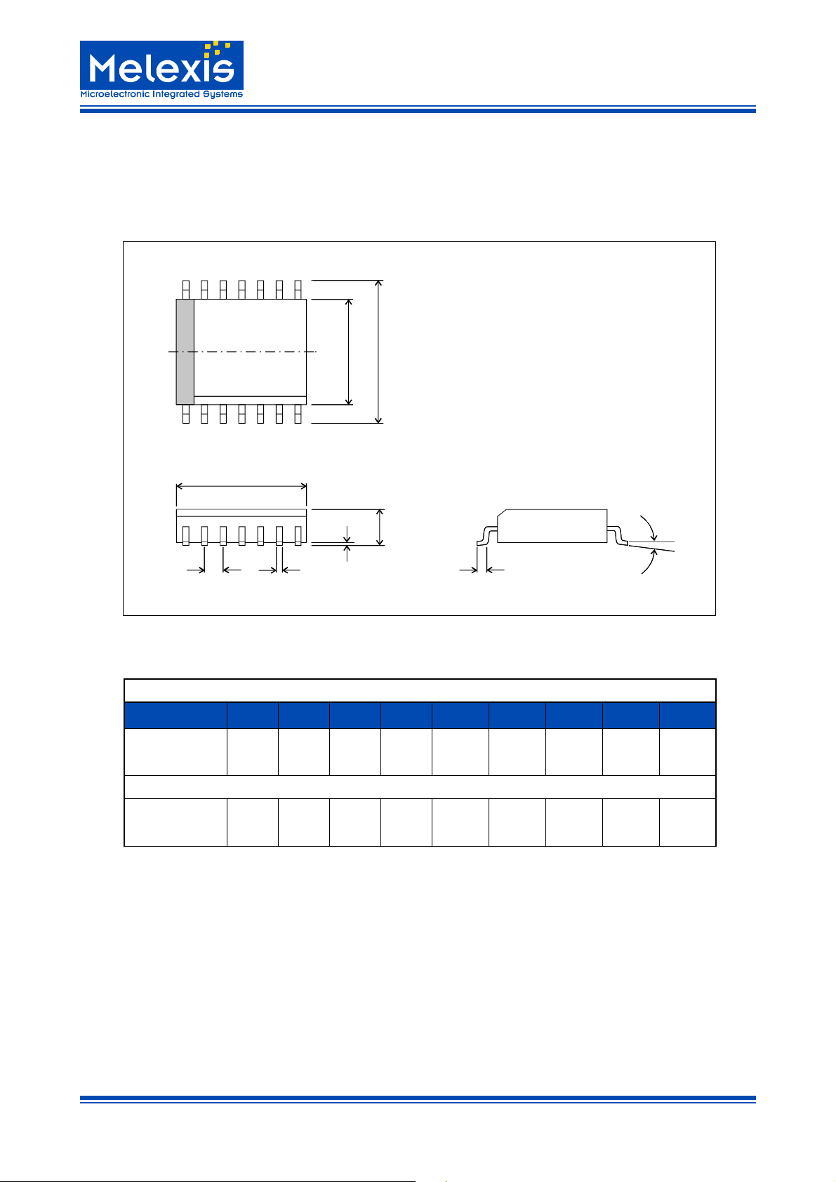
Mechanical Specifications
SOIC16 Package Dimensions
123
TH3122
EH
D
A1 A
e
b
L
Small Outline Integrated Circiut (SOIC), SOIC 16, 300 mil
All Dimension in mm, coplanarity < 0.1 mm
D E H A A1 e b L
min
max
All Dimension in inch, coplanarity < 0.004”
min
max
10.1
10.5
0.398
0.413
7.40
7.60
0.291
0.299
10.00
10.65
0.394
0.419
2.35
2.65
0.093
0.104
0.10
0.30
0.004
0.012
1.27
0.050
0.33
0.51
0.013
0.020
0.40
1.27
0.016
0.050
α
αααα
0°
8°
0°
8°
www.melexis.com Page 12 Datasheet Rev 1.0 July 2001
Page 13

TH3122
K-Bus Transceiver with integrated Voltage Regulator
www.melexis.com Page 13 Datasheet Rev 1.0 July 2001
Page 14

TH3122
K-Bus Transceiver with integrated Voltage Regulator
For the latest version of this document, go to our website at:
www.melexis.com
Or for additional information contact Melexis direct:
Europe
All other locations
Phone: +1 603 223 2362
E-mail: [email protected]
Important Notice
Devices sold by Melexis are covered by the warranty and patent indemnification provisions appearing in its Term of Sale. Melexis makes no warranty,
express, statutory, implied, or by description regarding the information set forth herein or regarding the freedom of the described devices from patent
infringement. Melexis reserves the right to change specifications and prices at any time and without notice. Therefore, prior t o designing this product into
a system, it is necessary to check with Melexis for current information. This product is intended for use in normal commercial applications. Applications
requiring extended temperature range, unusual environmental requirements, or high reliability applications, such as military, medical life-support or lifesustaining equipment are specifically not recommended without additional processing by Melexis for each application.
The information furnished by Melexis is believed to be correct and accurate. However, Melexis shall not be liable to recipient or any third party for any
damages, including but not limited to personal injury, property damage, loss of profits, loss of use, interrupt of business or indirect, special incidental or
consequential damages, of any kind, in connection with or arising out of the furnishing, performance or use of the technical data herein. No obligation or
liability to recipient or any third party shall arise or flow out of Melexis’ rendering of technical or other services.
© 2000 Melexis GmbH. All rights reserved.
www.melexis.com Page 14 Datasheet Rev 1.0 July 2001
 Loading...