

Page 1
Features and Benefits
TH3044
www.melexis.com
Page 1 Datasheet Rev 1.1 July 2001
q Open-emitter output with slew rate control
q Quiescent current < 50mA
q Bus voltage range -16 V .. +30 V
q ISO 9141 and OBDII compliant
q Wide temperature range -40 .. 125 °C
q SOP-14 or SOP-8 package
q Baudrate 9600
q Automotive applications
Ordering Information
Part No. Temperature Range Package
TH3044.3A -40ºC...125ºC SOIC14, 150mil
TH3044 JDC -40ºC...125ºC SOIC8
K-Bus Interface
General Description
The TH3044 is a bidirectional bus interface
device for data transfer from 5V to 12V supply.
For proper functionality control units are
implemented.
This interface device was especially designed
for automotive applications.
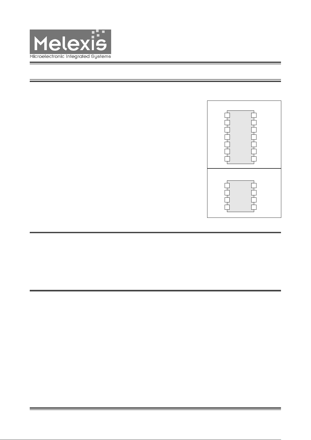
Pin Diagram
SOIC14NB
TH3044
1
VCC
GND
RXD
NRXD
BUS
VBAT
SEN/STA
TxD
14
13
12
11
10
9
87
6
5
4
2
3
TH3044
1
VCC
GND
RXD
NRXD
BUS
VBAT SEN/STA
TxD
8
7
6
54
2
3
SOIC 8
Page 2
TH3044
K-Bus Interface
www.melexis.com
Page 2 Datasheet Rev 1.1 July 2001
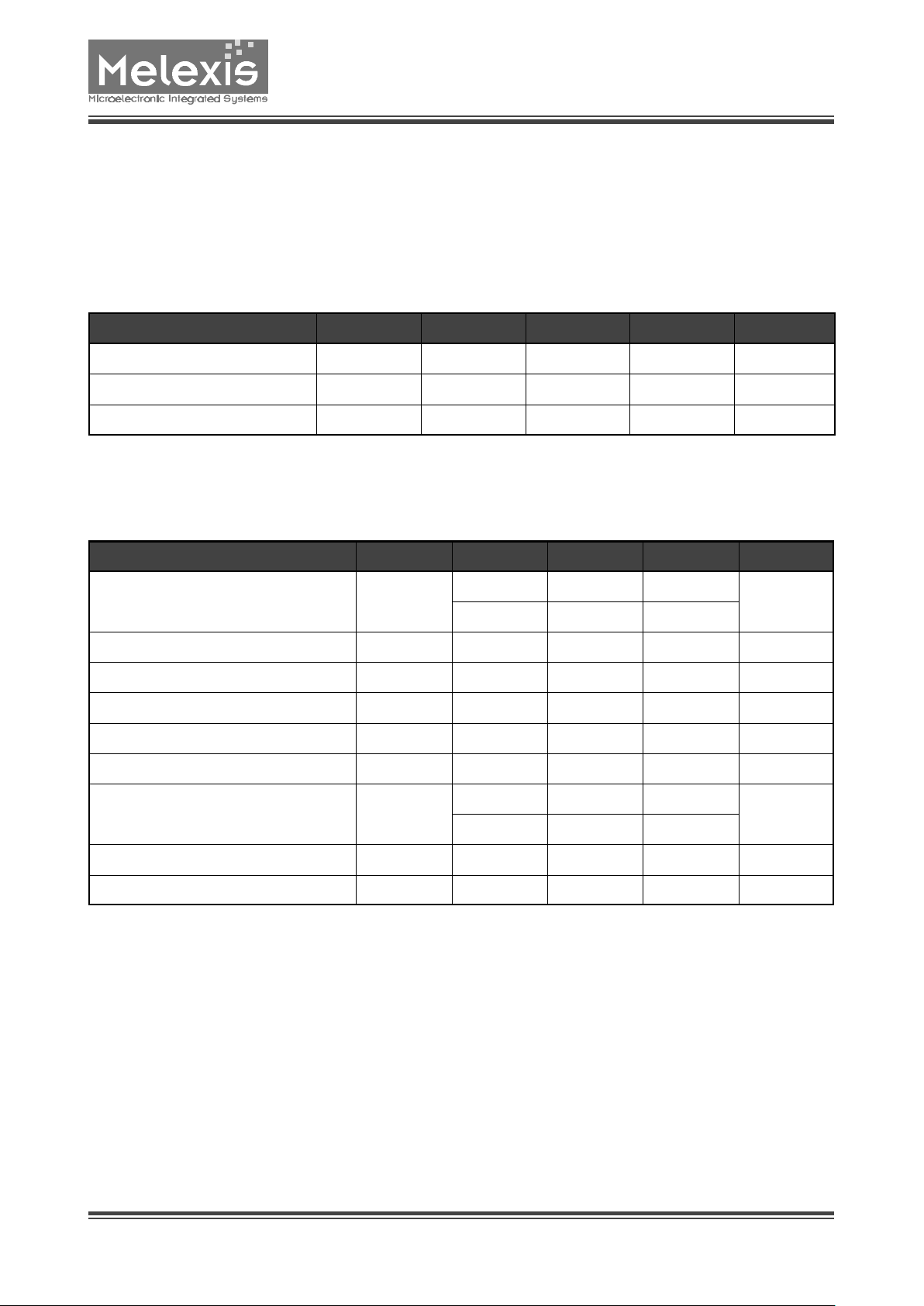
All voltages are referenced to ground (GND). Positive
currents flow into the IC. The absolute maximum ratings
(in accordance with IEC 134) given in the table below are
limiting values that do not lead to a permanent damage
of the device but exceeding any of these limits may do
Electrical Characteristics
Absolute maximum ratings
so. Long term exposure to limiting values may affect the
reliability of the device. Reliable operation of the TH3044
is only specified within the limits shown in ”Operating
conditions”
Operating Conditions
Parameter Symbol Min Typ Max Unit
Battery Voltage V
BAT
6 16 V
Supply Voltage VCC 4.5 5.5 V
Operating Temperature TA -40 125 °C
Parameter Symbol Condition Min Max Unit
Battery Voltage V
BAT
-0.3 30
V
T ≤ 500 ms
40
Battery Current I
BAT
20 mA
Supply Voltage VCC 7 V
Supply Current ICC 10 mA
Input Voltage SEN/STA,TxD VIN -0.3 VCC+0.3 V
Input Current SEN/STA, TxD IIN -10 10 mA
Input Voltage BUS V
INBUS
-16 30
V
T ≤ 500 ms
40
Output Current RxD, NRxD I
OUT
-10 10 mA
Operating Temperature TA -40 125 °C
Page 3

TH3044
K-Bus Interface
www.melexis.com
Page 3 Datasheet Rev 1.1 July 2001
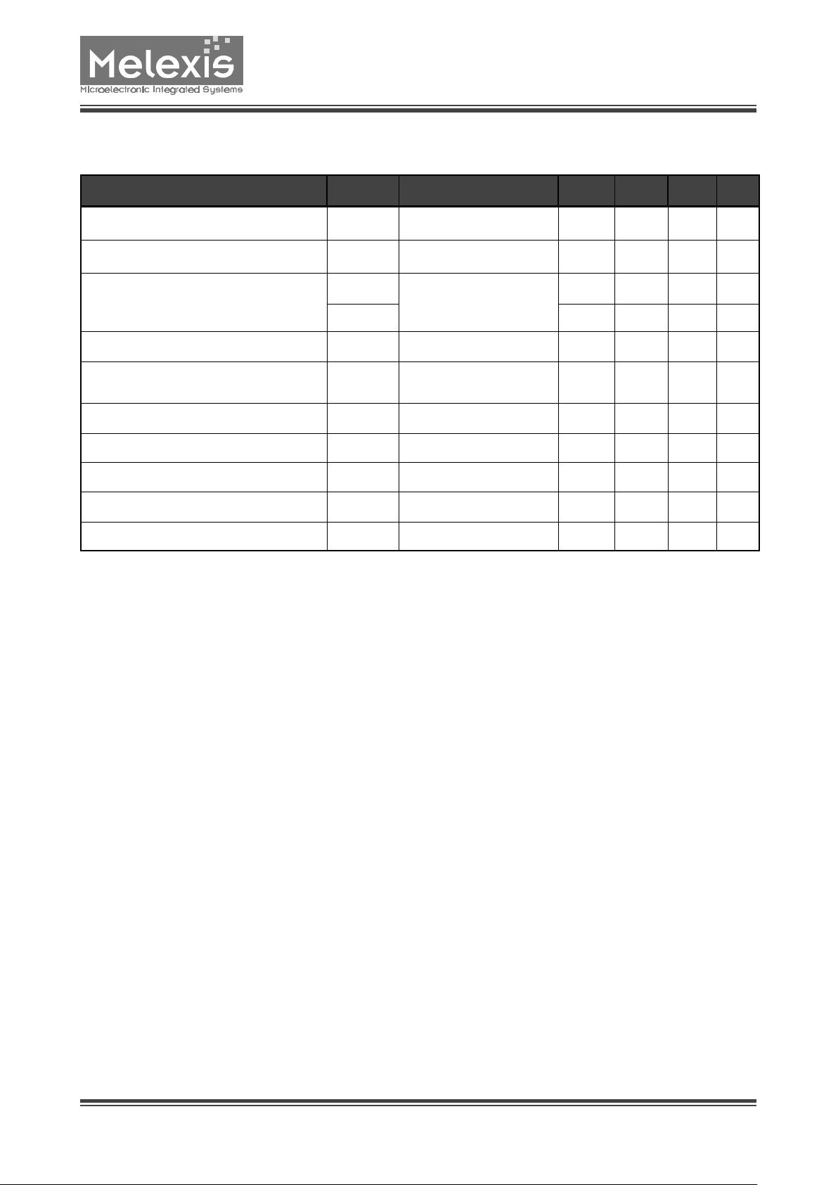
Static Characteristics
VDD= 4.5 to 5.5V, V
Bat
= 6 to 16V, T
amb
= -40°C to +125°C, unless otherwise specified
Parameter
Symbol Condition Min Typ Max Unit
Supply
Power-on-reset Threshold VCC V
CCPOR
3.0 4.0 V
Power-on-reset Threshold VBAT V
BATPOR
3.0 4.5 V
Quiescent Current, ICC + IBAT I
CCBAT
VCC = 5V, VBAT = 12V,
BUS, TxD, SEN/STA, RxD
and NRxD open
50
µA
TxD, SEN/STA, RxD, NRxD
Pull-up Current TxD Ipu -330 -250 -170
µA
Pull-down Current SEN/STA I
pdSEN
170 250 330
µA
Pull-up Current SEN/STA I
puSEN
-330 -250 -170
µA
Input Voltage Low TxD, SEN/STA VIL 0.25 VCC
Input Voltage High TxD, SEN/STA VIH 0.75 VCC
Output Voltage Low RxD, NRxD VOL I
OUT
= 1 mA 1 V
Output Voltage High RxD, NRxD VOH I
OUT
= 1 mA VCC -1.0 V
BUS
Input Voltage Low BUS VIL 0.45 V
BAT
Input Voltage High BUS VIH 0.55 V
BAT
Hysteresis Input Voltage V
HYS
50 mV
Input Resistance BUS R
IN
V
BAT
= 0..40V 400 600 1500
kΩ
V
BAT
= 0..40V, TA = 85°C 1300
kΩ
V
BUS
= 12V 60
kΩ
Output Voltage BUS V
BUS
VBAT = 12V,
SEN/STA = Low,
I
BUS
= 40mA
1.2 V
I
BUS
= 25mA 1.0 V
Output Sinking Current BUS (current
limiting)
I
LIM
V
BUS
> 3.5V 40 110 mA
Output Sinking Current BUS (before fold
back)
I
BUS
180 mA
Page 4
TH3044
K-Bus Interface
www.melexis.com
Page 4 Datasheet Rev 1.1 July 2001
Dynamic Characteristics
Parameter
Symbol Condition Min Typ Max Unit
Propagation Delay TxD -> RxD, NRxD tpd 20
µs
Threshold Voltage Fold-Back VFB 3.0 V
Slew Rate BUS
dV/dTfall
-2.2 -1.6 -1.0
V/µs
dV/dTrise 1.0 1.6 2.2
V/µs
Symmetry of Slew Rate BUS dV/dTsym 0.3
V/µs
Debouncing Time BUS
t
debH
t
debL
High or Low Pulse 1.5 2.8 4.0
µs
Symmetry of Debouncing Time BUS t
debsym
0.5
µs
Bit-Compare Time BUS, SEN/STA, TxD tbc 35 52 70
µs
Recover Time BUS, TxD t
rec
30 50 75
µs
Enable Time for transmit path BUS, TxD t
ena
0.92 1.33 1.8 ms
Constant-Low Time BUS, TxD t
low
3 6 12 ms
Page 5
TH3044
K-Bus Interface
www.melexis.com
Page 5 Datasheet Rev 1.1 July 2001
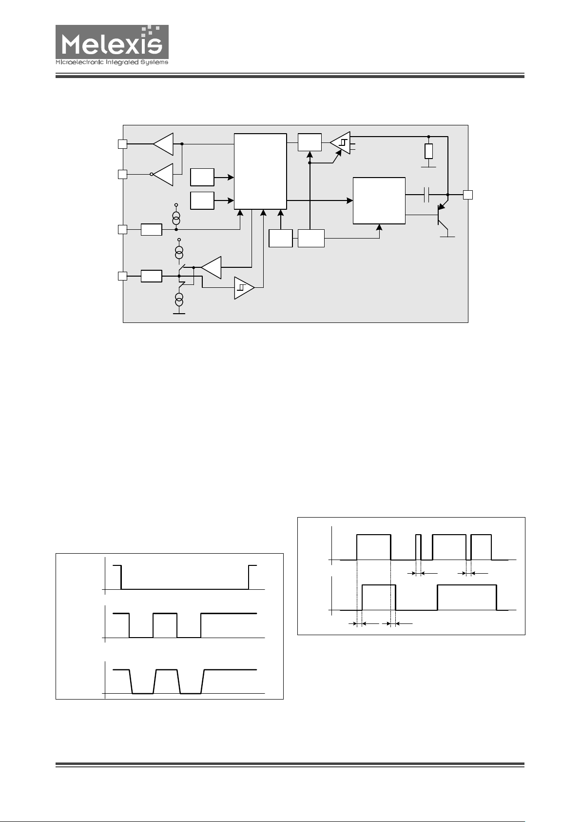
Functional Diagram
Figure 1 - Block Diagram
POR
VBAT
POR
VCC
Control-
logic
Bit-Compare
Constant-Low
VCC
ESD
ESD
VCC
OSC
Vref
Biasing
t
DEB
pnp Control
- slew rate
- I
B
- foldback
V
thH
V
thL
RxD
NRxD
TxD
SEN/STA
BUS
Functional Description
The TH3044 is used as a K-Bus interface. It
builds the connection between the serial 5V
bus line and the 12 V bus line. To avoid losses
of data informations control functions are
implemented.
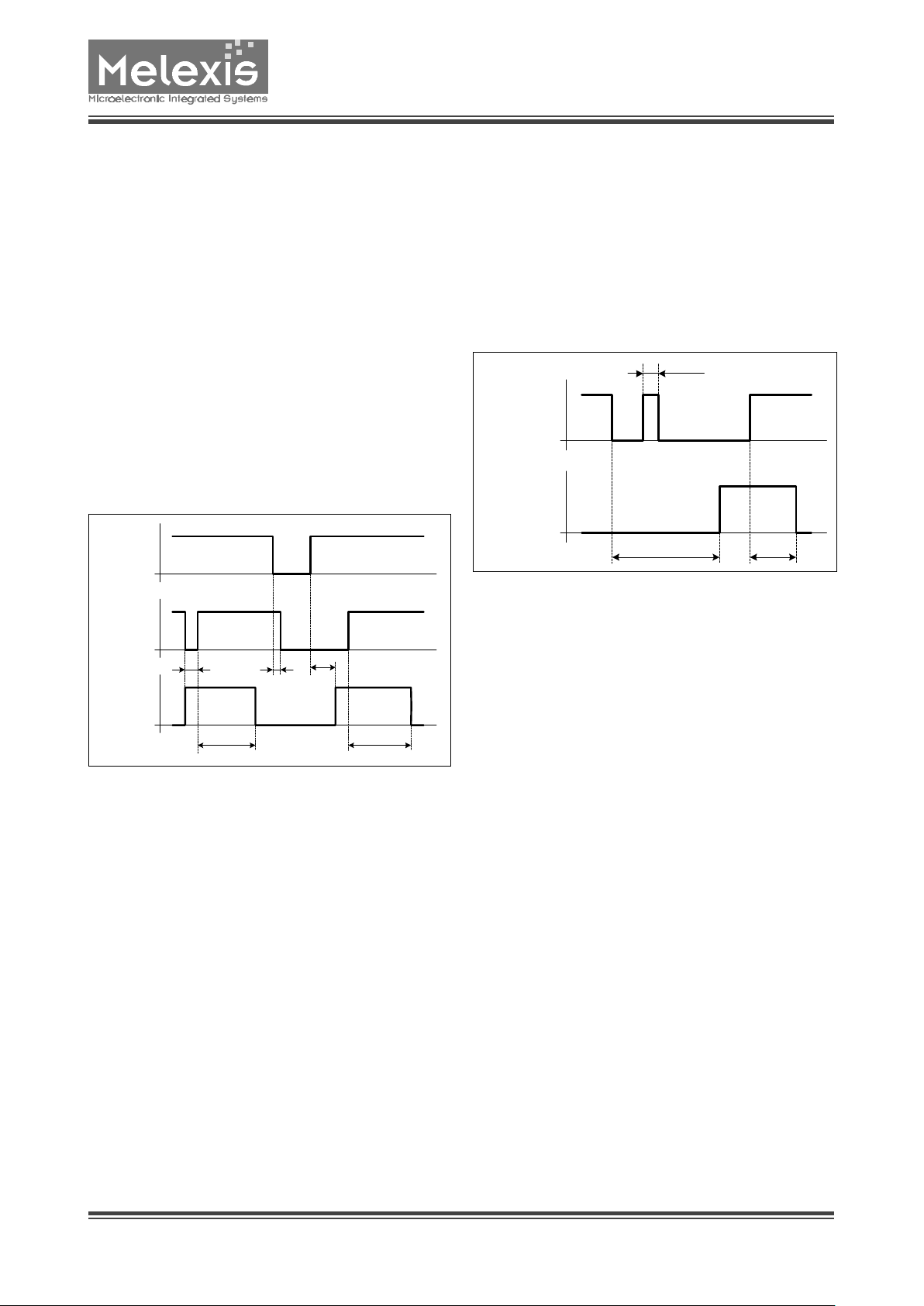
Transmit
During the transmission the data at the pin
TxD will be transferred to the pin RxD (NRxD)
as well as to the pin BUS.
SEN/STA
TxD
BUS
To minimise the electromagnetic emission of
the bus line, the slew rate of the rising and
falling edges of the data signals are limited.
Receive
The receiving path is always transparent.
Independent of the mode the pin RxD and
NRxD (inverted) are related to signal at the pin
BUS. Voltage spikes on the bus signal are
sup-pressed by the implemented debouncing
circuit.
BUS
RxD
t
debH
t
debL
< t
debH
< t
debL
Page 6
TH3044
K-Bus Interface
www.melexis.com
Page 6 Datasheet Rev 1.1 July 2001
Bit Compare
Are the signals at the pin TxD and the pin BUS
within a specified time t bc not identical, the
transmission will be interrupted.
If both signals at TxD and BUS are “High”
within the time t ena the transmission will be
enabled. To switch the TH3044 into the
receive mode a low level “0” has to be applied
to the pin Bus. If the TH3044 is part of a
complex bus system the first device which
transmits a low level “0” to the bus line forces
all other TH3044 to switch into the receive
mode. This state is valid until t
ena
.
The bitcompare-function is frequently retriggered by every new bit-comparison of two
different levels.
The bit-compare-function is activ when the pin
SEN/STA is open (not overwritten).
BUS
RxD
t
ena
t < t
bc
SEN/STA
t
ena
t
bc
Constant Low
A falling edge at pin TxD (from “1” to “0”) starts
the internal constant low timer.
If the low level “0” is valid for the time t low the
transmission unit of the TH3044 will be
disabled.
The receive unit is still active. A high level “1”
at TxD with a minimum pulse width of t resets
the constant low timer.
TxD
SEN/STA
t
low
t
ena
t < t
rec
SEN/STA
The pin SEN/STA is bidirectional. Used as an
output the pin indicates whether the transmitpath is enabled or disabled:
SEN/STA =”0”
transmission path is enabled
SEN/STA =”1”
transmission path is disabled
Using this pin as an input the transmission
path can be overwritten (independent of bitcompare and constant-low function):
SEN/STA=”0”
forcing the transmission path free
SEN/STA=”1”
disable the transmission path
Undervoltage
Undervoltage at pin VBAT or pin VCC doesn’t
occur an unwanted low level at pin Bus (see
chapter “Transmit”)
Page 7
TH3044
K-Bus Interface
www.melexis.com
Page 7 Datasheet Rev 1.1 July 2001
Application Information
Connecting Supply Pin’s
Connecting VBAT, VCC and GND in random
sequence does not cause damaging of the
device. The absence of VBAT-, VCC- or GNDconnection either alone or in any combination
does not influence or disturb the bus.
Reset
The pin BUS remains in tri-state, until internal
RESET state is released.
Reverse Protection
To protect the TH3044 from reverse voltages,
evers protection diode needs to be connected
to pin VBAT.
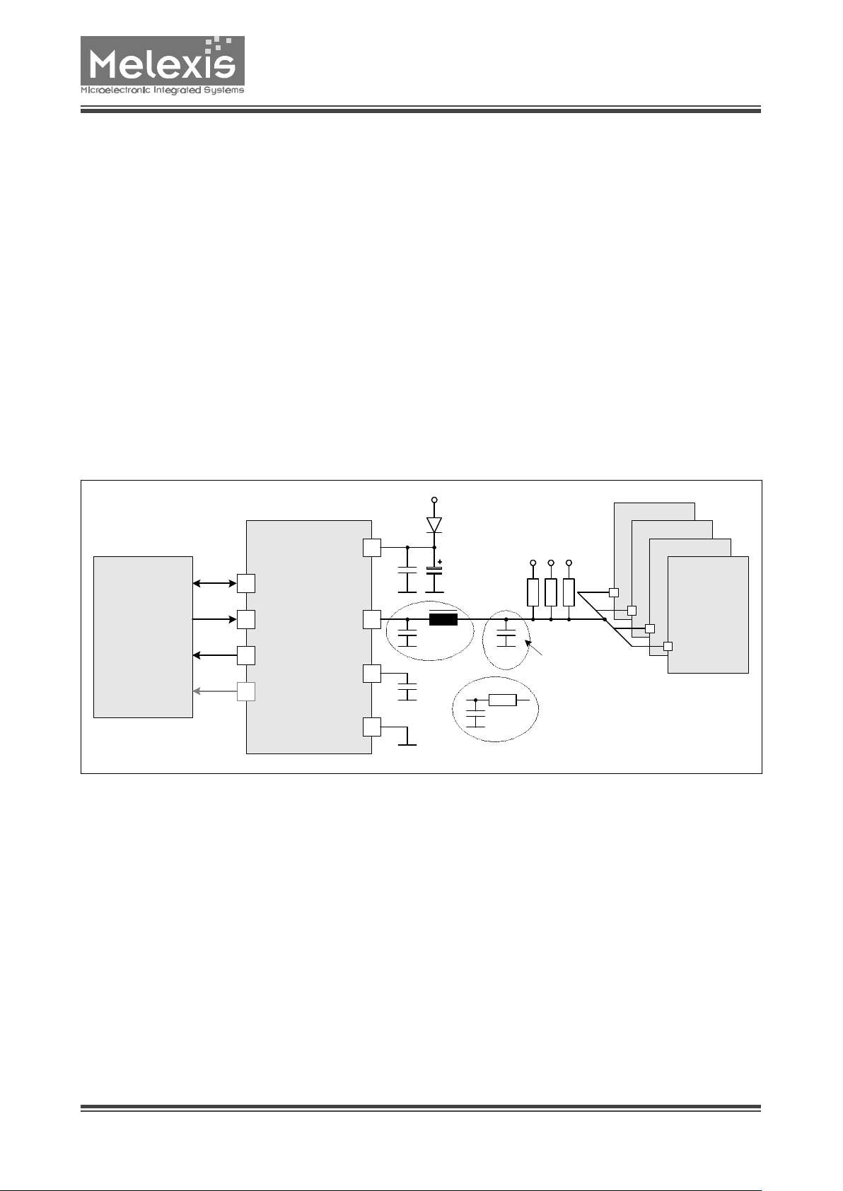
EMC Filter
In order to minimise EMC radiation a LC filter
(22 mH, 100 pF) is recommended. As an
option a RC filter (10 Ω, 100 pF) can be also
used.
Application Circuit
SEN/STA
TxD
RxD
NRxD
VBAT
BUS
VCC
GND
TH3044
MCU
TH3044
TH3044
TH3044
TH3044
V
Bat
V
Bat
10Ω
100p
optinal
RC-EMC Filter
EMC Filter
22uH
100p
BUS pullups
Rpu > 350Ω
100n 2.2u
100n
100p...220p
optinal
for improving ESD
Performance
Page 8
TH3044
K-Bus Interface
www.melexis.com
Page 8 Datasheet Rev 1.1 July 2001
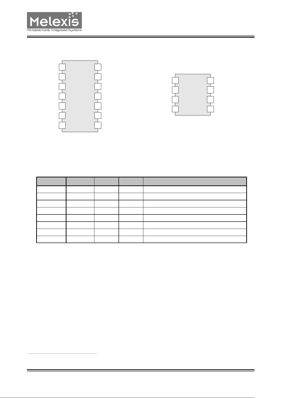
Pin Description
Pin SOIC14 Pin SOIC 8 Name I/O Function
3 1 GND P Ground
4 2 VCC I Supply Voltage 5V
6 3 BUS I/O K-Bus
7 4 VBAT P Battery Voltage
10 5 SEN/STA I/O Transmit Status
11 6 TXD I Transmit Input
13 7 RXD O Receive Output
14 8 NRXD O Inverted Receive Output
TH3044
1
VCC
GND
RXD
NRXD
BUS
VBAT
SEN/STA
TxD
14
13
12
11
10
9
87
6
5
4
2
3
TH3044
1
VCC
GND
RXD
NRXD
BUS
VBAT SEN/STA
TxD
8
7
6
54
2
3
SOIC 14 NB
SOIC 8
[1]
[1]
only available on request
Page 9
TH3044
K-Bus Interface
www.melexis.com
Page 9 Datasheet Rev 1.1 July 2001
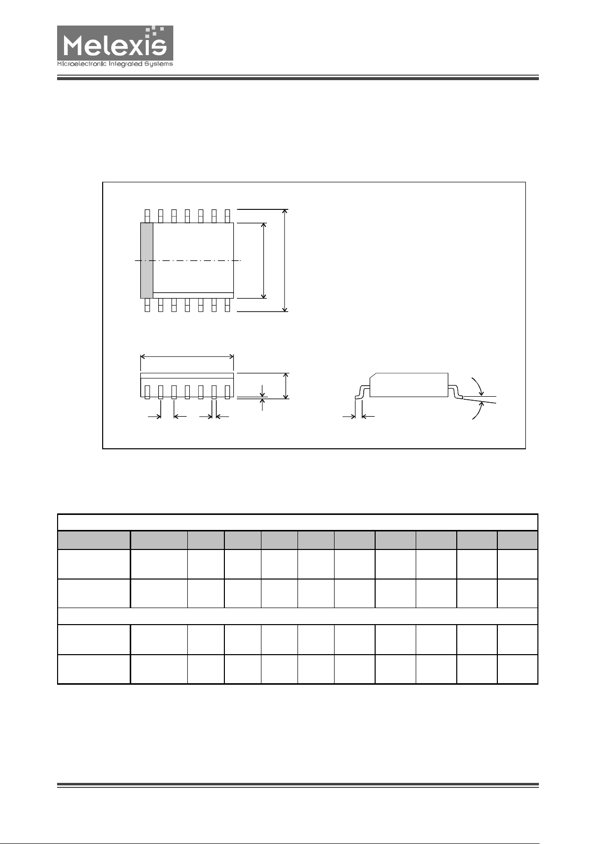
Mechanical Specifications
SOIC8 and SOIC14B Package Dimensions
1 2 3
D
E H
be
A1 A
L
α
Small Outline Integrated Circiut (SOIC),
All Dimension in mm, coplanarity < 0.1 mm
D E H A A1 e b L αα
min
max
4.8
5.0
3.80
4.00
10.00
10.65
5.80
6.20
0.10
0.25
1.27
0.33
0.51
0.40
1.27
0°
8°
min
max
0.189
0.197
0.150
0.157
0.228
0.244
0.053
0.069
0.004
0.010
0.050
0.013
0.020
0.016
0.050
0°
8°
All Dimension in inch, coplanarity < 0.004”
SOIC 8
150 mil
SOIC 8
150 mil
SOIC 14
150 mil
min
max
8.55
8.75
3.80
4.00
5.80
6.20
1.35
1.75
0.10
0.25
1.27
0.33
0.51
0.40
1.27
0°
8°
SOIC 14
150 mil
min
max
0.337
0.334
0.150
0.157
0.228
0.224
0.053
0.069
0.004
0.010
0.050
0.013
0.020
0.016
0.050
0°
8°
Page 10

TH3044
K-Bus Interface
www.melexis.com
Page 10 Datasheet Rev 1.1 July 2001
Devices sold by Melexis are covered by the warranty and patent indemnification provisions appearing in its Term of Sale. Melexis makes no warranty,
express, statutory, implied, or by description regarding the information set forth herein or regarding the freedom of the described devices from patent
infringement. Melexis reserves the right to change specifications and prices at any time and without notice. Therefore, prior to designing this product into
a system, it is necessary to check with Melexis for current information. This product is intended for use in normal commercial applications. Applications
requiring extended temperature range, unusual environmental requirements, or high reliability applications, such as military, medical life-support or lifesustaining equipment are specifically not recommended without additional processing by Melexis for each application.
The information furnished by Melexis is believed to be correct and accurate. However, Melexis shall not be liable to recipient or any third party for any
damages, including but not limited to personal injury, property damage, loss of profits, loss of use, interrupt of business or indirect, special incidental or
consequential damages, of any kind, in connection with or arising out of the furnishing, performance or use of the technical data herein. No obligation or
liability to recipient or any third party shall arise or flow out of Melexis’ rendering of technical or other services.
© 2000 Melexis GmbH. All rights reserved.
Important Notice
For the latest version of this document, go to our website at:
www.melexis.com
Or for additional information contact Melexis direct:
n Europe
Phone: +32 13 67 04 95
E-mail: [email protected]
n All other locations
Phone: +1 603 223 2362
E-mail: [email protected]
 Loading...