

Page 1
TH6503
USB Low-Speed Interface
Description
Features
TH6503 Sample
Application
The TH6503 is an integrated circuit which enables
the Universal Serial Bus (USB) to be connected to
a microcontroller. The interface module contains
all the components required to transmit data via
the USB.
The TH6503 has been developed for applications
requiring a low speed interface to the USB. Any
microcontroller can be used for control purposes.
In addition to the default endpoint 0 for control
transfer up to two endpoints can be supported by
TH6503. The TH6503 has been developed in
conformity with USB Specifications 1.1.
? Complient with USB Specification 1.1
? Supports up to three programmable endpoints
for interrupt and control transfer in each direction
? Data transfer at USB low speed
? Supports suspend mode
? Universal serial microcontroller interface
? Register programmable
? Programmable 1.5 MHz to 6 MHz out clock for
microcontroller
? Provides power supply for the microcontroller
(3.3 volts or 5 volts)
? Integrated oscillator for clock generation,
supports 6 MHz quartz, ceramic resonator
or external clock input
? Simple external circuitry
TH6503
Interface
to USB
Host / Hub
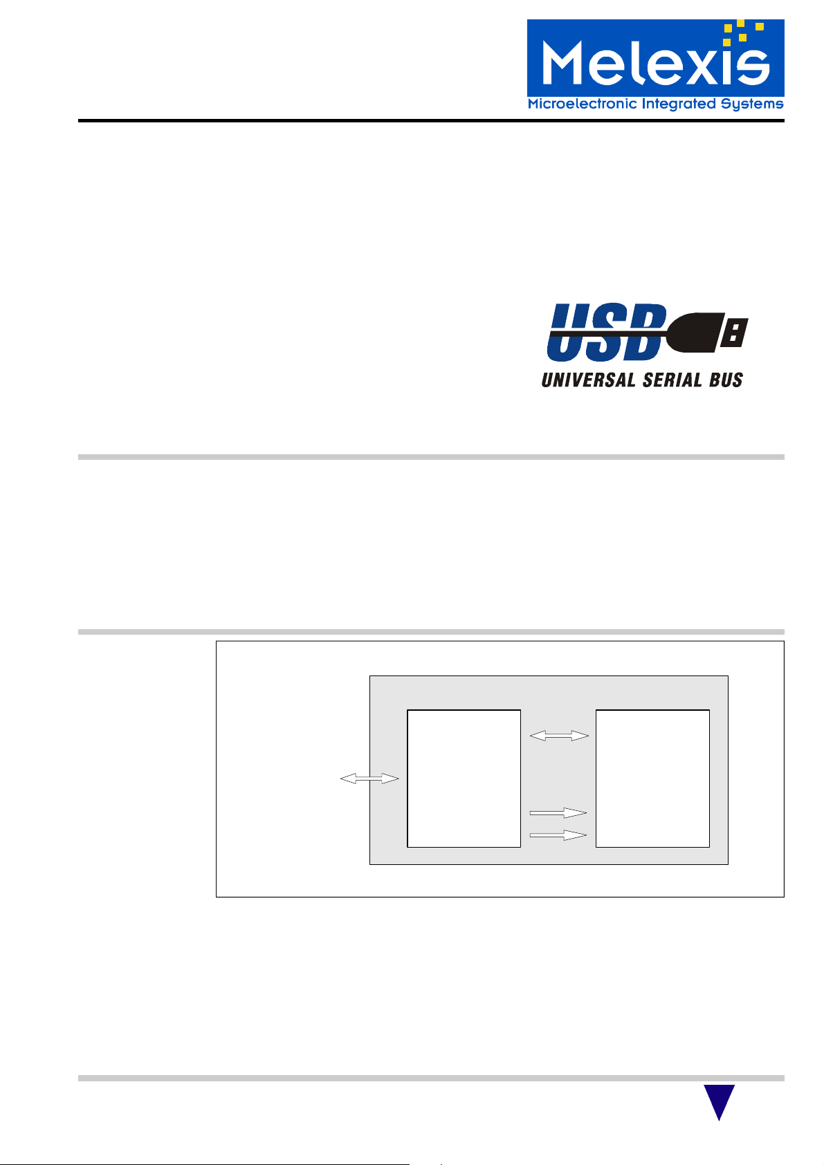
Figure 1. Typical TH6503 Sample Application
Figure 1 demonstrates a typical TH6503 application. The TH6503 translates the data and control
signals received from the USB in a serial format
which can be read by the microcontroller. The data
is stored in a FIFO buffer and can be called up from
a standard microcontroller via a register programmable serial interface at any time and processed
further. Data generated by peripheries is passed
Rev. 3.5
Dec 2000
USB
Interface
OCLK
/ORST
Serial
Microcontroller/
Customer
Application
to the TH6503 with the same protocol and stored
in a FIFO buffer until it is collected by the USB. The
TH6503 translates all the data in the USB-specific
format and generates the necessary control signals. The TH6503 requires a minimum number of
external elements and can easily be implemented
in a circuitry. It provides an external clock which
can be used to activate a microcontroller.
Page 2

TH6503 USB Low-Speed Interface
Function USB Data Transmission
The TH6503 supports the USB Specification 1.1
data model.
Data from the USB host to the device and vice
versa is transmitted serially. The data are NRZI
coded to increase transmission reliability; bit
stuffing (inserting an extra 0 bit after any
6 consecutive 1 bits) is performed and a CRC check
carried out. Bit stuffing, NRZI coding/decoding and
CRC checks or generation are performed within the
TH6503.
The data is transmitted in packets. Three types of
packets are defined for the USB: token, data and
handshake.
TH6503/
Microcontroller
Cooperation
to USB
Hub/Host
USB
Interface
TH6503
Interrupt
Transfer
Control
Transfer
Endpoint 2
Endpoint 1
Endpoint 0
The token is always passed on by the host.
It contains a PID (packet identifier) which defines the
direction of the following data transmission and the
address of the device and endpoints to be addressed.
Depending on the previous token command, data is
transferred from the USB host to the TH6503 (OUT
transfer) or transferred from the TH6503 to the USB
host (IN transfer). In the process the respective
FIFOs are written (OUT) or read (IN).
The data transfer is concluded with a handshake.
If the data has been received successfully, an ACK
is sent to the data source. If no data is ready for an
IN transfer out of the TH6503, it sends an NAK
handshake instead of the data (if endpoint is enabled).
serial
Data
Micro-
controller
Vendor specific
Data
Input
Device
Figure 2. Data Flow
The TH6503 is responsible for the data flow between the USB and the microcontroller. It ensures
that the USB transfers the data in line with the
protocol. All information in the protocol layer is
decoded by the TH6503 and carried out accordingly.
The data arriving from the USB host is stored in a
FIFO buffer until it is collected by the microcontroller.
Data transmitted to the USB host are imported
from a FIFO buffer which has previously been filled
by the microcontroller. A /INT signal signals to the
microcontroller that the FIFO status has been
changed by USB.
Data is transferred between the microcontroller
and the TH6503 via a software-emulating serial
interface controlled by the microcontroller.
As the TH6503 cannot interpret the content of the
data, it must be evaluated within the microcontroller.
This also applies to USB-specific control information. All USB-typical descriptors and the associated requests must be created and managed by
the microcontroller.
The setting of the USB address serves here as an
example. After resetting the USB, the address is
set to the default value 0 (USBAddressRegister). A
specific address is transferred from the USB host
software to the device with the SET_ADDRESS
command. This command, like all SET and GET
commands, can only be decoded by the microcontroller. The USB address is decoded in the
TH6503 with the aid of the USB AddressRegister.
For this reason the microcontroller must write the
USB address determined in this register.
The TH6503 supports the USB suspend mode.
Control takes place via the microcontroller. The
ACT bit can be used in the StatusRegister <5>
which is set on the USB for each activity. If this bit
has been inactive for a longer period of time (3 ms),
the microcontroller can set the TH6503 and itself in
the suspend mode using the SUS bit in the
BridgeConfigRegister <4>. The suspend mode
can be ended using the software or an external
signal. Apart from the suspend mode, the TH6503
also supports a number of other power saving
modes which either stop the microcontroller by
switching off the clock or set the whole USB bridge
in a power saving mode.
The TH6503 provides the clock pulse for the
microcontroller. It can be programmed with the
OCR 1 - OCR 0 bits in the BridgeConfigRegister
<1-0>.
The TH6503 supplies 3.3V voltage to power the
microcontroller; this is produced by the adjacent
5V bus power supply connection.
2
Page 3
TH6503 USB Low-Speed Interface
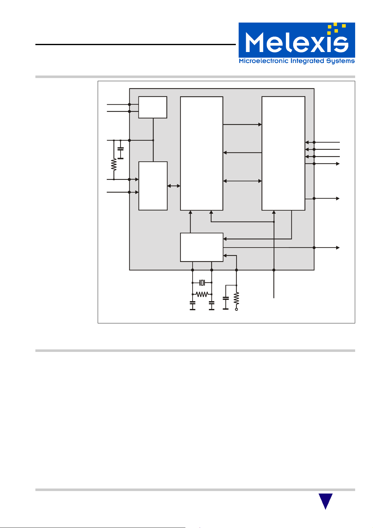
OCLK
SCK
SIN
SDI
SDO
1312111015816
Power
14
/ORST
Micro-
controller
TH6503/
Microcontroller
Cooperation
(continued)
VBus
GND
V3.3
D-
D+
1k5
10µ
1
5
Supply
3.3V
SIE
2
Serial
Interface
Engine
3
4
USB
I/O
Status Signals
Control Signals
Interface
Bus Interface
Microcontroller
Interface
Oscillator/
Divider
6
Figure 3. TH6503 Block Diagram
The data is transferred between the microcontroller and the USB bridge using the clock (SCK)
generated by the microcontroller asynchronous to the USB clock.
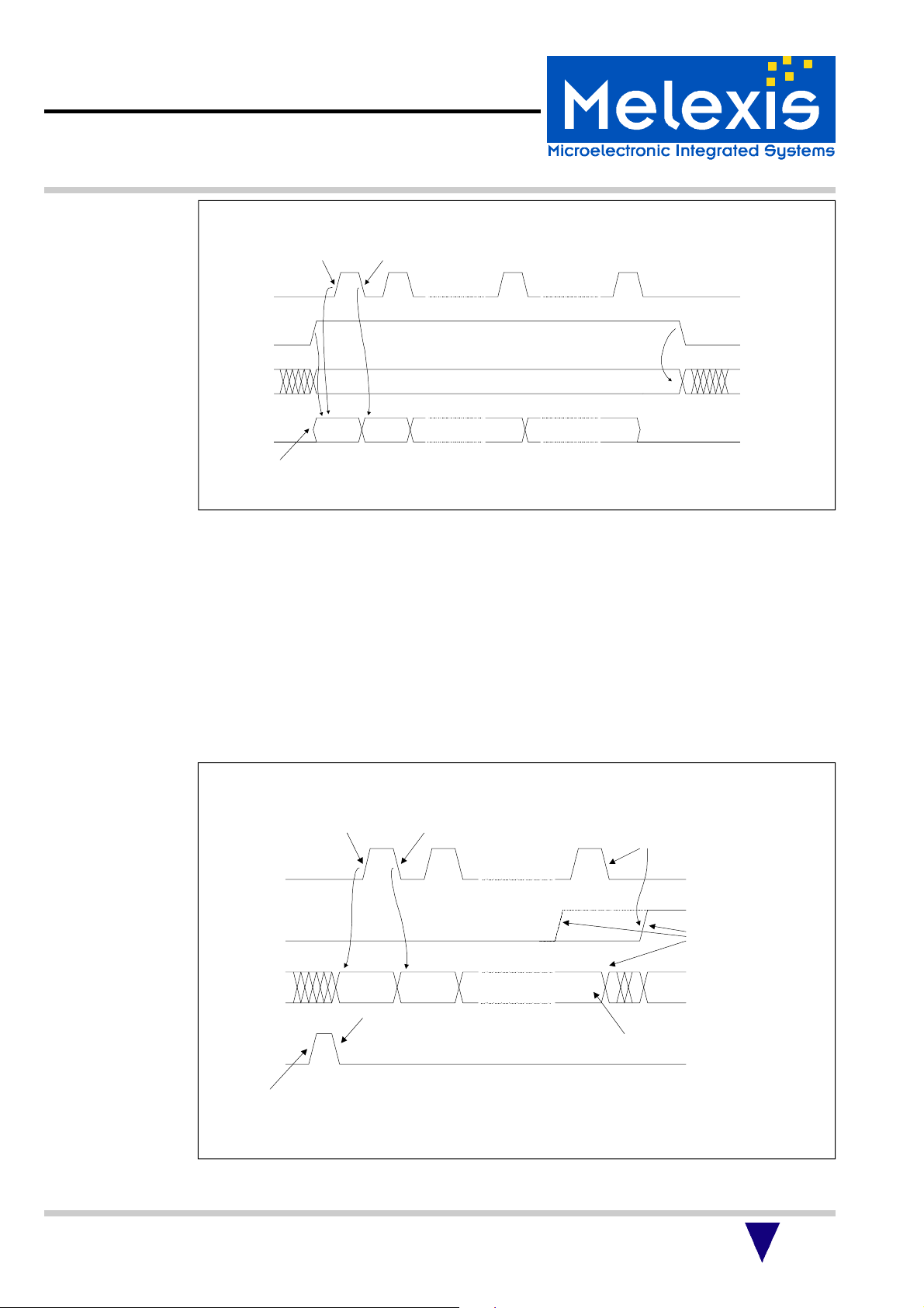
Data IN Transfer
(from the microcontroller to the TH6503)
Data IN transfer is initiated with rising SIN edge (IN
packet sync). Data is transferred via the SDI pin.
Initially the Adr/CntInRegister which indicates the
internal address in the TH6503 is written. Data is
subsequently transferred beginning with byte 0 to
Byte n LSB first. Bits IC3-IC0 in the Adr/CntInRegister
<3-0> contain the information on the number of
bytes to be transferred to the USB host if the target
of the data transfer was an IN FIFO.
A zero data transfer is identified with reset of IC3IC0 bits after writing the Adr/CntInRegister one
additional clock on SCK must be generated.
7
WAKE
RESET
V3.3
If a register is the target of the data IN transfer the
bits IC3-IC0 and TI have no meaning.
With falling SCK edge the microcontroller transmit the bits to SDI and the bits are imported from
the bridge with increasing SCK edge. After each
transmission of 8 bits the respective IN FIFO value
is increased by 1. If the microcontroller writes
more data than indicated in the Adr/CntInRegister,
the oldest data are overwritten. After the final
falling edge of SCK first SDI and then SIN must be
reset to 0 to terminate the transfer. The associated
IN Done bit in the StatusRegister is reset automatically to enable USB IN transfer.
3
Page 4
TH6503 USB Low-Speed Interface
Microcontroller
Interface
(continued)
SCK
SIN
SDO
Figure 4. Serial Data IN
Bridge latches
Data on rising
edge of SCK
1
0
1
0
1
0
1
SDI
0
Microcontroller outputs
Adr/CntInRegister Bit 0 / AC0
on SDI
Microcontroller shifts
Data on falling
edge of SCK
0 1 7 n+8
End of IN Transfer
/INT
AC7 Data Bit 0 Bit nAC0 AC1 AC2
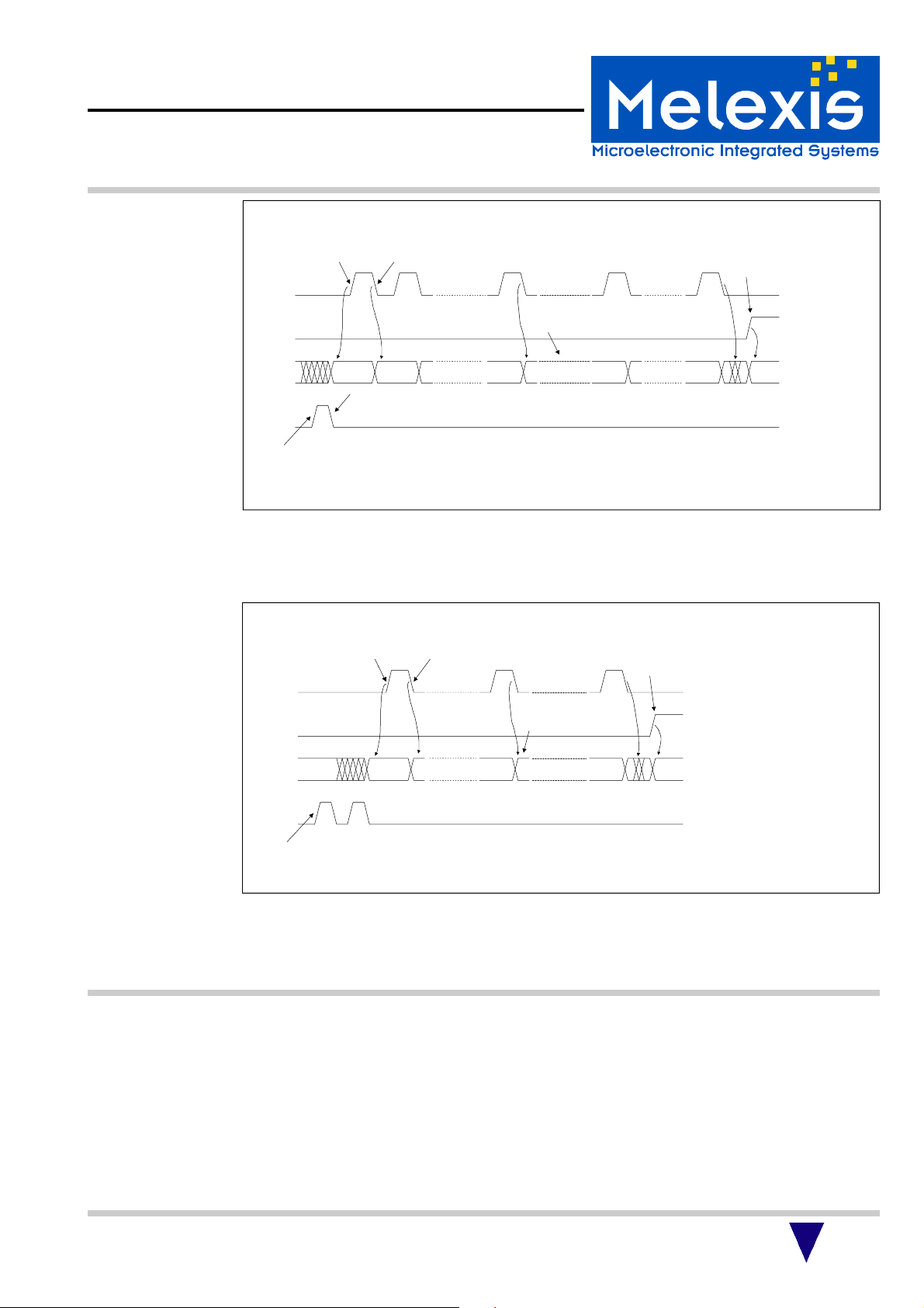
Data OUT Transfer
(from the TH6503 to the microcontroller)
An impulse on the SDI link at SIN = 0 represents
the OUT packet sync for an OUT transfer. With the
falling SCK edge the data (LSB first) is shifted to
SDO and with rising SCK edge accepted by the
microcontroller. The StatusRegister is transferred
initially followed by the CntOutRegister and finally
the OUT FIFO data. If the transfer is terminated after
less than 8 clock pulses, only single StatusRegister
bits are read. Linear transfer is interrupted by SIN
Bridge shifts
Data on falling
edge of SCK
0 1 n
Clear Interrupt Latch
SCK
SIN
SDO
SDI
1
0
1
0
1
0
1
0
Microcontroller
latches Data
on rising edge
of SCK
Status0 Status1 Status2 Status n /INT
= 1 and must be initiated with a new OUT packet
sync at SIN = 0. Two impulses on the SDI link
initiate a transfer of the CntOutRegisters and of the
following OUT FIFO bytes without the
StatusRegister. A zero data transfer is identified by
an OUT Count Byte value of 0. The end of a Data
OUT transfer clears the SET bit in the
CntOutRegister and the OD bit in the
StatusRegister to make the next USB OUT or
Setup transfer possible.
End of
Transfer
any break
after identify the
/INT source possible
n <= 7
SDI pulse with SIN=0:
- copy StatusRegister to Shift Register for Serial Data Out
Figure 5. OUT Transfer of StatusRegister
4
Page 5
TH6503 USB Low-Speed Interface
Microcontroller
Interface
(continued)
Microcontroller
latches Data
on rising edge
of SCK
1
SCK
0
1
SIN
0
1
SDO
0
1
SDI
0
SDI pulse with SIN=0:
- transfer StatusRegister to Serial Data Out
Figure 6. Complete Data OUT Transfer
Bridge shifts
Data on falling
edge of SCK
0 1 7 15 n+16
Status0 Status1 Status2 Status7 CNT0 CNT7 FIFO Bit 0 Bit n /INT
Clear Interrupt Latch
Bridge outputs
next Register (CntOutRegister)
Bit 0 on SDO
End of OUT Transfer
(OUT Tranfer after reading
the Status -and CntOutRegister
with SIN=0 clears
EP0 Out Done
Interrupt Function
Microcontroller
latches Data
on rising edge
of SCK
1
SCK
0
1
SIN
0
1
SDO
0
1
SDI
0
Two SDI pulses with SIN=0:
- transfer CntOutRegister and OUT FIFO Bytes
to Serial Data Out
Bridge shifts
Data on falling
edge of SCK
0 7 n+8
Bridge outputs
next Register (FIFO)
Bit 0 on SDO
CNT0 CNT1 CNT7 FIFO Bit 0 Bit n /INT
End of OUT Transfer
(OUT Tranfer > 8 clocks
the Status -and CntOutRegister
with SIN=0 clears
EP0 Out Done
Figure 7. OUT Transfer, only CntOutRegister and OUT FIFO Bytes
If SIN = 1, the SDO pin can be used to generate an
interrupt signal. The interrupt is low active. It is
triggered if a control transfer is made from the USB
host or a control or interrupt transfer is made to the
USB host and one of the ID12, ID0 or OD bits has
been set in the StatusRegister <3-1> or at high
level of the WAKE pin. An interrupt signal is also
triggered on RESUME and USB_RESET.
The interrupt latch is reset on reading the status
register. If an interrupt is generated during reading StatusRegister, this interrupt is latched and
the interrupt source is after new StatusRegister
reading visible.
A WAKE interrupt is only generated during the stop
state (bits SO and/or SMC in the BridgeConfig
Register are set).
5
Page 6
TH6503 USB Low-Speed Interface
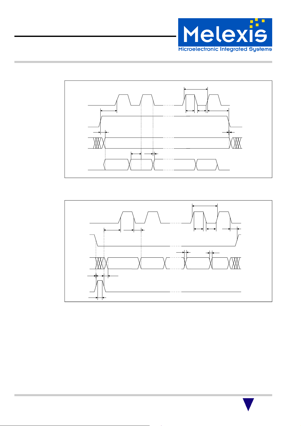
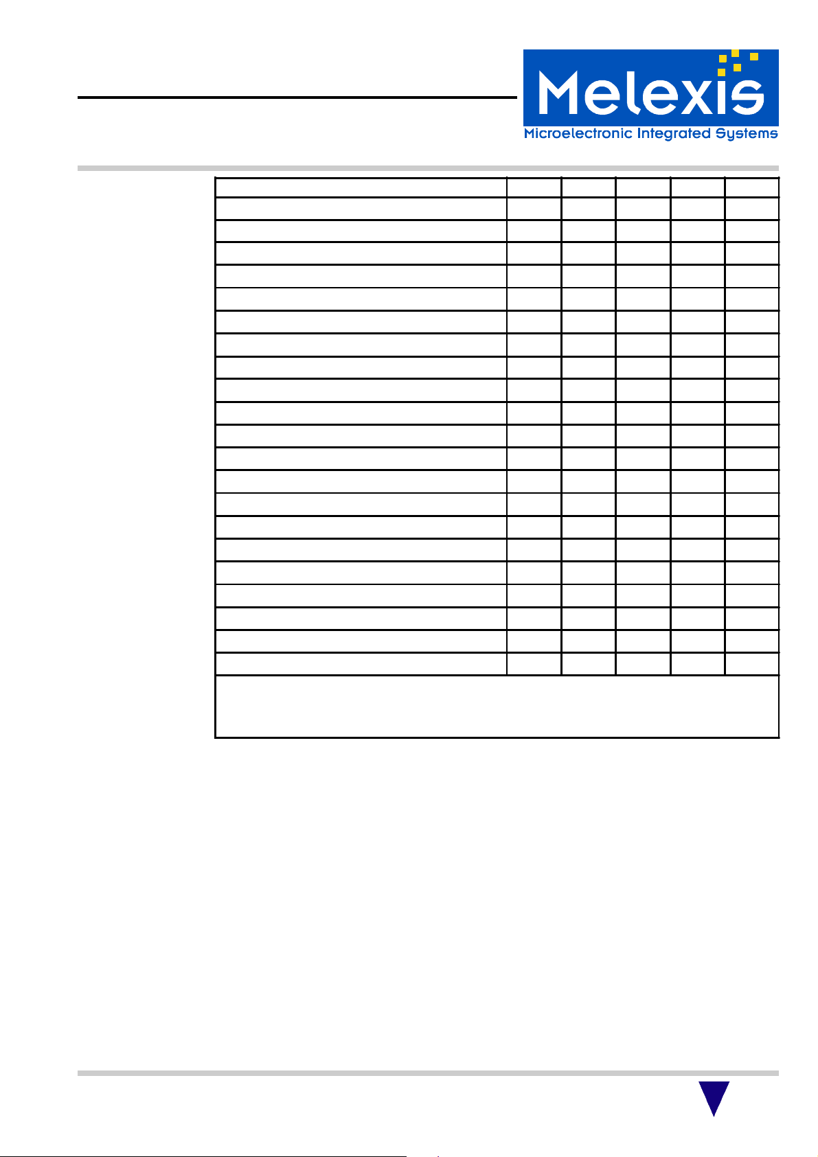
Timing Serial
Interface
Figure 8 and Figure 9 show the timing of the serial interface of the TH6503. The serial interface is
controlled by a standard microcontroller. It can be connected with any microcontroller port.
t
3
SCK
t
t
6
t
4
t
5
7
SIN
SDO
SDI
t
8
/INT
t
10t11
Bit 0 Bit n
t
9
Figure 8. Timing Serial Data IN
t
3
SCK
t
t
16
17
SIN
SDO
t
12
Bit 0 Bit n
t
15
SDI
t
14
Figure 9. Timing Serial Data OUT
t
t
4
t
1
t
5
13
t
2
6
Page 7
TH6503 USB Low-Speed Interface
Timing Serial
Interface
(continued)
Description [1] Symbol Unit min typ max
General
Oscillator Input period on OSC1 ns 164 170
Rising time of SDO t
Falling time of SDO t
SCK period t
High time SCK [2] t
Low time SCK [2, 3] t
1
2
3
4
5
ns 20
ns 7
ns 600 Step
ns 345
ns 255
Data IN
Setup time of SCK after rising edge of SIN t
Hold time of SIN after last rising edge of SCK t
Setup time of INT-Signal after rising edge of SIN t
Hold time of INT-Signal after falling edge of SIN t
Setup time of Data on SDI before rising edge of SCK t
Hold time of Data on SDI after falling edge of SCK t
6
7
8
9
10
11
ns 170
ns 170
ns 200
ns 165
ns 170
ns 0
Data OUT
Setup time of SDI-pulse after falling edge of SIN t
Setup time of SIN after last falling edge of SCK t
High time of SDI-pulse t
Setup time of Data on SDO after falling edge of SDI-pulse t
Setup time of SCK after falling edge of SDI-pulse t
Setup time of Data on SDO after falling edge of SCK t
12
13
14
15
16
17
ns 170
ns 170
ns 255
ns 280
ns 170
ns 365
Notes:
[1] Capacitive load of 50 pF
[2] Can be asymmetrical
[3] The low time of SCK between the last bit of a byte and the first bit of the next byte must be at least 510 ns.
Input signals are double buffered and digital filtered. Therefore all spikes with a width < 255 ns are
suppressed.
7
Page 8

TH6503 USB Low-Speed Interface
Connecting the
TH6503 with a
Microcontroller
The TH6503 can be connected with any microcontroller via a serial interface. The serial outputs
can be connected with any microcontroller ports.
The TH6503 out clock can be used to provide the
clock pulse supply to the microcontroller. The
TH6503
SCK
SIN
SDI
SDO
OCLK
13
12
11
10
15
MC6805
PA0
PA1
PA2
PA3
XOSC1
XOSC2
/ORST
Figure 10. The Connection between the
14
V
3.3
TH6503 and the
MC6805 by Motorola
/RESET
reset output is low active and configured in an
open drain structure. For this reason the output
must be set at a defined level with external V
resistance.
TH6503
SCK
SIN
SDI
SDO
OCLK
13
12
11
10
15
Z86Kxx
P24
P25
P26
P27
XTAL1
XTAL2
/ORST
Figure 11. The Connection between the
14
V
3.3
TH6503 and the Z86Kxx by Zilog
/RESET
3.3
TH6503
SCK
SIN
SDI
SDO
OCLK
13
12
11
10
15
80C51
P1.0
P1.1
P1.2
P1.3
XTAL1
XTAL2
/ORST
Figure 12. The Connection between the
14
V
3.3
TH6503 and the 80C51 by Intel
RST
TH6503
SCK
SIN
SDI
SDO
OCLK
13
12
11
10
15
PIC16C5x
RA0
RA1
RA2
RA3
OSC1
OSC2
/ORST
Figure 13. The Connection between the
14
V
3.3
TH6503 and the
PIC16C54 by Microchip
/MCLR
8
Page 9

TH6503 USB Low-Speed Interface
Application
Wiring Diagram
Figure 14 shows a sample Application circuitry with the TH6503 and a MC68HC05.
To stabilize the internal power supply the V3.3 pin must always be connected with an 10µ capaci-
tor.
Figure 14. Sample Wiring diagram to connect the TH6503 with an MC68HC05
WAKE Function
The USB specification defines that a device has to
go into suspend mode if no bus traffic was detected for ca. 3 ms. After the device is set to
suspend mode, the WAKE pin can be used to
Wake up the device with an external event.
If the WAKE pin is connected with an RC-Element,
the TH6503 wakes up after the time defined by the
RC-Element. This feature can be used to check for
data in periodical time frames.
RESET Output
The reset output (/ORST) of the TH6503 can be
connected with the reset input of the
microcontroller. It’s a low active signal.
This signal has a minimum length of 31 clock
cycles with a default frequency of 1.5 MHz (see Pin
Description for details).
After this reset pulse the microcontroller can
reseted but it must wait to programming the
TH6503 until the USB reset is inactive.
All register of TH6503 will be held in reset state,
exept the StatusRegister, until the corresponding
bits HWR or RES is cleared.
9
Page 10

TH6503 USB Low-Speed Interface
Register
Description
The StatusRegister, CntOutRegister and the OUT FIFO can only be read by the microcontroller.
The internal Registers of the TH6503 can only be written by the microcontroller.
StatusRegister (read only)
always the first byte of a data out transfer
is loaded in the out shift register with the falling edge of an pulse on SDI with SIN=0
Bit
Number
7 HWR 1
6 RES 0
5 ACT 0
4 RDT 0
3 ID12 0
2 ID0 0
1 OD 0
0 WA 1
Bit
Mnemonic
Reset
Status
Function
Hardware Reset
is set if the reset source is POR, RESET pin or low voltage reset
?
is reset automatically on reading the StatusRegister and also by the following
?
SW-Reset before reading the StatusRegister
USB Reset
?
is set so long as a reset is received on the USB (SW reset)
?
is reset automatically on reading the StatusRegister and also by the following
HW-Reset before reading the StatusRegister
?
the reset of this bit enables EP0 Out and EP0 In (EO0 and EI0 bits in the
SerialFlag Register are set)
USB Activity
?
is set when the USB is active (all bus states exept IDLE)
?
is reset automatically on reading the StatusRegister
?
can be used by the microcontroller to calculate the suspend time
?
if set the SO and SMC bits in the BridgeConfigRegister are reset
USB Resume Detect
?
is set automatically if a resume status has been decoded
?
is reset automatically if the resume status has been terminated
?
if set the SO and SMC bits in the BridgeConfigRegister are reset
EP1/2 IN Done
is set if the data requested by an IN token have been completely
?
transmitted to the USB host and an ACK has been received
is reset with the falling SIN edge (end of IN transfer)
?
EP0 IN Done
??is set if data requested by an IN token have been completely
transmitted to the USB host and an ACK has been received
is reset with the falling SIN edge (end of IN transfer)
OUT Done
??is set automatically if the data are complete in the FIFO after a valid
SETUP or OUT token has been received and an ACK has been sent
to the USB host
is reset with the rising SIN edge (end of OUT transfer)
WAKE Activity
is set and reset automatically depending on the voltage level at the
?
WAKE pin
is an inverted copy of the WAKE pin and can be used as low active
?
interrupt output, when SIN = 1
10
Page 11

TH6503 USB Low-Speed Interface
Register
Description
(continued)
CntOutRegister (read only)
second byte of each out transfer following an OUT packet sync
Bit
Number
7-6 OA 0
5 TO 0
4 SET 0
3-0 OC3-0 0
Bit
Mnemonic
Reset
Status
Function
OUT Address
last valid OUT endpoint
?
indicates the endpoint of actual OUT FIFO data
00 EP0
01 EP1
10 EP2
?
only valid if EP1 OUT or EP2 OUT enabled, otherwise the internal
Revision number is visible
Toggle OUT
??is set if the data packet PID was DATA1 and reset if the data packet
PID was DATA0
is latched with a valid EP0 SETUP or a OUT Token
Setup
?
is set if a SETUP token is received
is reset after OUT transfer to microcontroller
?
no STALL or NAK is sent because it is not permitted on the SETUP
?
token
the SO0 and SI0 (STALL EP0) flags in the USBFlagRegister are reset
?
on rising edge of Setup
?
a SETUP token flash all IN FIFOs
EP0 OUT Byte Count
amount of OUT data received in the EP0 FIFO in bytes
applicable values from 0 to 8
?
?
a zero data transfer is identified 0
Internal Register
Adr/CntInRegister (write only)
first byte of each data in transfer following the IN packet sync
Bit
Number
7 TI 0
6-4 RA2-0 0
3-0 IC3-0 0
Bit
Mnemonic
Reset
Status
Function
Toggle IN
? is set if the data packet PID is DATA1 and reset if the data packet PID
is DATA0
Internal Address
destination address for a write operation to a TH6503 register or IN
FIIFO
IN Byte Count
number of data bytes to be transmitted without Adr/CntInRegister from
the microcontroller to the TH6503 if the destination address was an IN
FIFO
?
applicable values from 0 to 8
?
0 indicates a zero data transfer to the USB host, but blocks the InFIFO
until ACK is received
11
Page 12

TH6503 USB Low-Speed Interface
Register
Description
(continued)
EP0/1/2 FIFO (write only)
Internal Address: b000, b001 or b010
Size: 8 bytes
The device user data is stored temporarily at this location for transfer to the USB host.
• the address b000 indicates a data transfer from EP0
• the address b001 indicates a data transfer from EP1
• the address b010 indicates a data transfer from EP2
• only one of the three addresses may be used at any one time; FIFO is used alternately, depending on the device function
• will be flushed with a new SETUP token for as long as bit SET in CntOutRegister is set
SerialFlagRegister (write only)
Internal address: b100
Size: 8 bits
All endpoints must remain deactivated until USB reset has been decoded (Statusregister <6>).
Bit
Number
7-6 X 0 reserved - must be set to 0
5 EO2 0
4 EO1 0
3 EI2 0
2 EI1 0
1 EI0 0
0 EO0 0
Bit
Mnemonic
Reset
Status
Function
Enable EP2 OUT
activate endpoint 2 OUT
Microcontroller can set the bit after detecting a USB reset in order to
?
enable data transfers from the USB host via EP2
If set the CntOut Register bit <7-6> indicates the source of the last OUT
?
transfer binary coded
Enable EP1 OUT
activate endpoint 1 OUT
?
Microcontroller can set the bit after detecting a USB reset in order to
enable data transfers from the USB host via EP1
?
If set the CntOut Register bit <7-6> indicates the source of the last OUT
transfer binary coded
Enable EP2 IN
activate endpoint 2 IN
Microcontroller can set the bit after detecting a USB reset in order to
?
enable data transfers to the USB host via EP2
Enable EP1 IN
activate endpoint 1 IN
?
Microcontroller can set the bit after detecting a USB reset in order to
enable data transfers to the USB host via EP1
Enable EP0 IN
activate endpoint 0 (IN transfer)
is set automatically after detecting a USB reset to enable IN control
?
transfers to the USB host
Enable EP0 OUT
activate endpoint 0 (OUT transfer)
is set automatically after detecting a USB reset to enable OUT control
?
transfers to the USB host
12
Page 13

TH6503 USB Low-Speed Interface
Register
Description
(continued)
USBFlagRegister (write only)
Internal address: b101
Size: 8 bits
Bit
Number
7 FI2 1
6 FI1 1
5 FI0 1
4 BO0 0
3 SI2 0
2 SI1 0
1 SI0 0
0 SO0 0
Bit
Mnemonic
Reset
Status
Function
Flush EP2 IN
clears EP2 FIFO
?
is set and reset automatically depending on the actual FIFO Status
must be set before EP2 of the EP1/2 FIFO can be overwritten by the
?
microcontroller
Flush EP1 IN
clears EP1 FIFO
is set and reset automatically depending on the actual FIFO Status
?
must be set before EP1 of the EP1/2 FIFO can be overwritten by the
?
microcontroller
Flush EP0 IN
clears EP0 FIFO
?
is set and reset automatically depending on the actual FIFO Status
?
must be set before the EP0 FIFO can be overwritten by the
microcontroller
Busy OUT
blocks the EP0 OUT FIFO for the USB host
is set and reset automatically depending on the actual FIFO Status
?
TH6503 responds with no handshake for a USB host SETUP token or
?
with a NAK signal for an OUT token (NAK state)
to leave the NAK state, the microcontroller does an OutFIFO read
?
(the microcontroller rereads the last data)
STALL EP2
sets EP2 to STALL
TH6503 responds with a STALL for a USB host IN or OUT token
?
if address and EP2 have been decoded
only operative if EP2 is active
?
STALL EP1
sets EP1 to STALL
?
TH6503 responds with a STALL for a USB host IN or OUT token
if address and EP1 have been decoded
?
only operative if EP1 is active
STALL EP0 IN
sets EP0 IN to STALL
TH6503 responds with a STALL for a USB host IN token
?
if address and EP0 have been decoded
will be cleared after SETUP token
?
STALL EP0 OUT
sets EP0 OUT to STALL
?
TH6503 responds with a STALL for a USB host OUT token
if address and EP0 have been decoded
?
STALL is inoperative for a SETUP token from the USB host
?
SETUP clears STALL EP0 IN and STALL EP0 OUT bits
USBAddressRegister (write only)
Internal address: b110
Size: 8 bits
Bit
Number
7 X 0 reserved
6-0 AD6-0 0
Bit
Mnemonic
Reset
Status
Function
USB device address
USB address entered by microcontroller
?
zero after reset
?
microcontroller must decode the address from descriptor data after a
SETUP (SET_ADDRESS) token and write it in this register
13
Page 14

TH6503 USB Low-Speed Interface
Register
Description
(continued)
BridgeConfigRegister (write only)
Bits only take effect after the data IN transfer
has been completed.
Internal address: b111
Size : 8 bits
Bit
Number
6 OS 0
5 FR 0
4 SUS 0
3 SO 0
2 SMC 0
1-0 OCR1-0 0 0
Bit
Mnemonic
Reset
Status
Function
OCLK Static
?
is set and reset by microcontroller
?
if set the OCLK pin drives a static level on the OCLK pin, this level
depends on the SMC bit in the BridgeConfigRegister
OS SMC OCLK Output
0 0 Clock, programmed by OCR<1-0> bits
0 1 0
1 0 0
1 1 1
?
can be used as ending stop state signal for an external microcontroller
with own clock
?
works like a low active interrupt
Force Resume
terminates suspend mode
is set by microcontroller if data is sent from connected device
?
the TH6503 signals a Resume to the USB host
?
the timing (10-15 ms) of the Resume State must be done by
?
microcontroller
Suspend
sets the TH6503 in suspend mode
?
should be set by the microcontroller if no bus traffic is detected for longer
than 3 ms
?
can be set and reset by microcontroller only
Stop Oscillator
stops the microcontroller and the USB bridge (the SMC bit is set
automatically)
is set by the microcontroller
?
is reset by an external wake up signal, USB activity or reset
?
Stop Microcontroller Clock
stops the microcontroller
is set by the microcontroller
?
is reset by an external wake up signal, USB activity or reset
?
only affects the OCLK pin
?
Out Clock Rate
output frequency on the OCLK pin
0 0 1.5 MHz (default)
0 1 2.0 MHz
1 0 3.0 MHz
1 1 6.0 MHz, without guarantee of symmetry, it depends on the
quality of the oscillation element
14
Page 15

TH6503 USB Low-Speed Interface
Flowchart for
Programming the
TH6503
Main Program
Figure 15 shows the main order of events of the USB specific part of firmware for the
microcontroller. The bits located in the StatusRegister mark the event. Depending on these bits the
firmware must branch.
Initialisation
SCK=0;SIN=1;
SDI=0
Yes
SDO=1
No
Read
StatusRegister
Read CntOutRegister
and OUT FIFO
Reaction (depends
on the received Data)
Yes
OUT Done
Data to send ?
Yes
Write next Control
Byte(s) to
IN FIFO
No
Data to send ?
Yes
Write next Device
Data to
IN FIFO
Reset SUS Bit in the
BridgeConfigRegister
Reset Suspend
Timer
YesNo
Yes
Yes
Yes
EP0 IN Done
No
EP1/2 IN Done
No
Resume Detect
No
USB Active
No
USB Reset
Yes
Figure 15. Flowchart for Main Program (using TH6503 in Interrupt mode)
15
Page 16

TH6503 USB Low-Speed Interface
Flowchart for
Programming the
TH6503
(continued)
Reading the StatusRegister
The Reading of the Status Register is the first action of the microcontroller. The TH6503 stores the
information on what’s happened on the USB in this Register
Read
StatusRegister
SIN=0
generating a pulse on
SDI
Generating a rising edge
on SCK to save bit on
SDO
Save SDO bit
more bits to read ?
abort transfer with
SIN=0
Figure 16. Reading the StatusRegister
No
Yes
Generating a falling
edge on SCK to shift
next bit to SDO
16
Page 17

TH6503 USB Low-Speed Interface
Flowchart for
Programming the
TH6503
(continued)
Reading the CntOutRegister and OUT FIFO
If the Out Done bit in the StatusRegister is set, the microcontroller must receive the data collected
from the OUT FIFO.
Read CntOutRegister
and OUT FIFO
continue after reading StatusRegister (see
Fig.6 and Fig 7 on page 5)
generating a rising edge
on SCK
save SDO bit
more bits to read ?
No
abort transfer with
SIN = 1
Figure 17. Reading the CntOutRegister and OUT FIFO
Generating a falling
Yes
edge on SCK to shift the
next bit to SDO
17
Page 18

TH6503 USB Low-Speed Interface
Flowchart for
Programming the
TH6503
(continued)
Reaction on the FIFO data
After the microcontroller has collected the FIFO data, the microcontroller must decode the FIFO data
and reacts appropriately.
Reaction
Setup bit = 1 ?
Decoding FIFO Data,
Reaction depends on
the request (see USB
Figure 18. Reaction on the received Data
Yes
Spec Rev. 1.1,
Chapter 9)
18
Page 19

TH6503 USB Low-Speed Interface
Flowchart for
Programming the
TH6503
(continued)
Write next Device Data to TH6503
If IN FIFO data has to be sent to the USB host the microcontroller must wait until the corresponding IN
DONE bit is set (IN FIFO is empty). Then the microcontroller can store the next data in the IN FIFO.
Write Adr/CntInRegister
Write next Device
Data to
IN FIFO 1 or 2
Write Internal Register
Write next Control
Byte(s) to
IN FIFO 0
SIN=1
output first bit on SDI
generating a rising edge
on SCK to latch bit by
bridge
more bits to write ?
No
End of IN Transfer
SIN=0 and SCK=0
Figure 19. Writing next Device or Control Data to IN FIFO
Yes
generating a falling edge on
SCK and output the next bit
on SDI
19
Page 20

TH6503 USB Low-Speed Interface
Electrical
Characteristics
All voltage values are referenced to GND (GND = 0 V). All values are based on the USB specification V1.1. If any value is unspecified, the value from the USB specification V1.1 is valid.
Absolute maximum ratings
Parameter Symbol Min Max Unit
DC supply voltage V
Input voltage V
Input Current I
Storage temperature range (ceramic) T
Storage temperature range (plastic) T
Power Dissipation (SOP16) P
DD
IN
IN
STGC
STGP
D
- 0.3 7.0 V
- 0.3 V3.3 + 0.3 V
- 10 10 mA
- 65 150 °C
- 40 125 °C
600 mW
Recommended Operational Conditions
Parameter Symbol Min Typ Max Unit
DC supply voltage V
Operating temperature range T
Junction temperature T
Operating Frequency f
DD
A
J
OP
4.40 5.00 5.25 V
0 70 °C
< 150 °C
6.00 MHz
20
Page 21

TH6503 USB Low-Speed Interface
Electrical
Characteristics
Static Characteristics
Parameter Symbol Condition [4] Min Typ Max Unit
Power supply voltage V
Power supply current I
Stand-by Current [5] I
Voltage input LOW V
Voltage input HIGH V
Schmitt trigger, positive going
threshold
Schmitt trigger, negative going
threshold
Hysteresis, Schmitt trigger
(VT+ – VT-)
Differential Input Sensitivity V
Differential Common Mode Range V
Single Ended Receiver Threshold V
Single Ended Receiver Hysteresis V
Input low current I
Input with pullup I
Input high current I
Input with pulldown I
Voltage output LOW V
Voltage output HIGH V
Current Output I
Differential output LOW V
Differential output HIGH V
Hi-Z Output Leakage Current I
ILCMOS
IHCMOS
V
T+CMOS
V
T-CMOS
V
HYSCMOS
3.3
3.3
STB
DI
CM
SE
HYSE
IL
ILU
IH
IHD
OL
OH
O
OLD
OHD
OZ
VIL to VIH,VIH to V
|(D+)-(D-)| 0.2 V
Includes V
DI
VIN = GND -10 10 µA
VIN = GND -50 -21.0 -7 µA
VIN = V3.3 -10 10 µA
VIN = V3.3 7 22.9 65 µA
IOL = 1 mA 0.4 V
IOH = 1 mA 2.4 V
RL of 15 KOhm
to GND
RL of 1.5 KOhm
to 3.6 V
VIN = GND
or V3.3
Notes:
[4] Specified at VDD = VBUS = 4.40V to 5.25V and tested at room temperature only
[5] Differential Transceiver fs in Suspend Mode, tested without pull-down and pullup Resistors
on the D- and D+ data line
3.00 3.30 3.60 V
80 150 µA
0.3*V
0.7*V
3.3
0.8 V
0.5 V
IL
0.8 2.5 V
0.8 2.0 V
0.1 V
2.8 3.6 V
-10 10 µA
60 mA
3.3
2.4 V
1 mA
0.3 V
V
V
21
Page 22

TH6503 USB Low-Speed Interface
Pin Description
Pin Description
USB Interface
1 VBus I adjacent 5V bus voltage
5 GND I Ground
4 D+ I/O USB data
3 D- I/O USB data
must be connected via 1.5 kOhm resistor to 3.3 V for low speed devices
?
Microcontroller Interface
13 SCK I Serial Clock (generated by microcontroller)
OUT transfer: SDO is accepted by the microcontroller in high status or with falling SCK edge.
?
The USB bridge shifts the next bit to SDO in low status or with rising edge.
IN Transfer: SDI is accepted by the USB bridge in high status or with falling SCK edge.
?
?
The microcontroller shifts the next bit to SDI in low status or with rising edge.
internal pulldown
?
12 SIN I Serial Input Direction (generated by the microcontroller)
specifies the direction of the data transfer and marks the end of a FIFO transfer
?
?
SIN = 0: data is sent from the USB bridge to the microcontroller via SDO. An OUT packet sync for the
StatusRegister or CntOutRegister can be triggered via SDI. A rising edge terminates a Status or OUT transfer
and the USB OUT Done status bit is cleared.
?
SIN = 1: Data is sent from the microcontroller to the USB bridge via SDI. SDO emits an /INT signal. A falling
edge terminates an IN transfer and the EP0 IN Done or EP1/2 IN Done status bit is cleared if the destination
address is a FIFO address.
rising edge indicates the commencement of an IN transfer (IN packet sync). The IN is started once SCK is
?
pulsed. The Adr/CntInRegister is transferred initially.
internal pulldown
?
11 SDI I Serial Data IN (from the microcontroller to the USB bridge)
?
generated by the microcontroller
SIN = 0: the falling edge from a single SDI impulse loads the first bit (LSB first) of the StatusRegisters to SDO.
?
The StatusRegister can be read. Two SDI impulses load the first bit of the CntOutRegister.
SIN = 1: SDI transfers the serial data.
?
?
internal pulldown
10 SDO O Serial Data Out (from the USB bridge to the microcontroller)
?
generated by the USB bridge
SIN = 0: SDO show the Status of bit 0 of the StatusRegister (WA) and after a SDI pulse SDO transfers the
?
serial data.
SIN = 1: SDO is used to generate the /INT signal which can be used to control the microcontroller interrupt
?
?
/INT:
- Low active signal to SDO at SIN 1
- is a NOR connection of the RESUME signal, USB reset and an interrupt latch
- Interrupt latch is set for all increases in OUTDone, EP0 IN Done and EP1/2 IN Done edge.
- Interrupt latch is reset, if the StatusRegister is read (SDI impulse at SIN= 0).
15 OCLK O Clock out for microcontroller (programmable frequency)
14 /ORST
Miscellaneous
6 OSC1 I Oscillator In for a quartz, ceramic resonator or external clock input, 6 MHz ± 1.5%
7 OSC2 O Oscillator Out
8 WAKE I
16 /RESET I RESET input with Schmitt-Trigger characteristic (internal pullup)
2 V3.3 O
9 TEST I
open
Reset Out (HW- or SW reset)
drain
?
ORST=0 reset state
?
ORST=1 normal operation
?
must be connected with an external pullup resistor (to V3.3)
?
all resets are indicated on this pin
?
this type of reset can be determined by evaluating the bits HWR or RES in the StatusRegister <7> or <6>
Reset conditions:
?
- internal POR
- RESET pin - min. 20µs (31 OCLK cycles at 1.5 MHz) or as long as the RESET pin is active
- Low voltage reset if VBUS<3.3V ± 10% with a minimum of 20 µs (31 OCLK cycles at 1.5 MHz) or as long as
VBUS < 3.3V
- USB-Reset - reduced to 20 µs (31 OCLK cycles at 1.5 MHz), the end of a USB reset is indicated by a rising
edge of /INT and by cleared RES bit in the StatusRegister
?
if a specific high trigger level is reached (Schmitt Trigger Characteristic) the USB bridge oscillator is restarted
and
?
the SO and SMC bit in the BridgeConfigRegister is cleared.
it may be connected to an RC element to achieve restart cycles from 50 to 100 ms
?
?
the input signal is compatible with large slew rate
if the SO or SMC bit in the BridgeConfigRegister is set a rising edge on the WAKE pin generates an interrupt
signal on SDO, when SIN = 0
3.3 V output
must be connected with an external capacitor (approx. 10µ)
Test pin, internal pulled up (do not connect to external circuitry)
?
22
Page 23

TH6503 USB Low-Speed Interface
T
Pinout
Information
(Top View)
VBUS
V3.3
D-
D+
GND
OSC1
OSC2
WAKE
1
2
3
4
TH6503
5
6
7
8
16
15
14
13
12
11
10
9
RESE
OCLK
/ORST
SCK
SIN
SDI
SDO
TEST
Package
Information
(SOP 16 WB)
The TH6503 is available in a SOP 16 WB Package.
E H
1 2 3
D
A1 A
be
Small Outline Package (SOP)
SOP 16 Wide Body (WB)
Package
type
SOP WB 16
Dimensions in inches, coplanarity < 0.004", original dimension: inch
SOP WB 16
Dimensions in millimeters, coplanarity < 0.1 mm, original dimension: inch
min
max
min
max
D E H A A 1 e b L
0.398
0.413
10.11
10.49
0.283
0.300
7.19
7.62
0.393
0.419
9.98
10.64
0.091
0.111
2.31
2.82
0.002
0.014
0.05
0.36
L
0.05
1.27
0.013
0.020
0.33
0.51
0.012
0.050
0.30
1.27
?
?
10 ° DF16
10 ° DF16
Package
code
Ordering
Information
Quality Data
The TH6503 USB Low-Speed Interface is available in a 16 pin SOP WB package.
The order number is TH6503.
Quality data is available on request. Contact: Thesys Mikroelektronik Produkte GmbH
Quality Assurance
Haarbergstr. 67, 99097 Erfurt, Germany
Tel.: +49-361-4276155, Fax: +49-361-4276060
23
Page 24

TH6503 USB Low-Speed Interface
Worlwide Sales Offices
For the latest version of this document,
Go to our website at:
www.melexis.com
Or for additional information
Contact Melexis Direct:
? USA
Melexis Inc.
41 Locke Road
Concord, NH 03301
USA
Phone: +1 603 223 2362
Fax: +1 603 223 9614
Email: sales_usa@melexis.com
?? Germany
Melexis GmbH
Schiess Strasse 55
D-40549 Dusseldorf,
Germany
Phone: +49 211 536-02-0
Fax: +49 211 536-02-50
Email: sales_de@melexis.com
? France
Melexis France
Tour Arago, 5 rue Bellini
92806 Puteaux La Defense
France
Phone: +33 147 78 11 34
Fax: +33 147 78 06 35
Email: sales_france@melexis.com
? Japan
Star Electronics Co., LTD
1-14-10 Shiba Minato-Ku,
Tokyo
Phone: +81 3 3452 7171
Fax: +81 3 3769 2197
Email: sales_japan@melexis.com
? United Kingdom
Silicon Concepts
PCB Lynchborough Road
Hampshire GU30 7SB
United Kingdom
Phone: +44 1428 751 617
Fax: +44 1428 751 603
Email: sales_uk@melexis.com
? Taiwan
Beechwood Int’l Taiwan Co.
Room 8, 17Floor, No.189, sec 2
Keelung Road
Taipei, Taiwan
Phone: +886 2 2739 3322
Fax: +886 2 2739 3090
Email: sales_taiwan@melexis.com
? Korea
NeoS Korea
Rm 205 chungho plaza, 668-9
Deungchon-dong, kangse-ku
Seoul 157-030
Phone: +82 2 3665 6527
Fax: +886 2 3665 6529
Email: sales_korea@melexis.com
Important Notice
Devices sold by Melexis are covered by the warranty and patent indemnification provisions appearing in its Term of Sale. Melexis makes
no warranty, express, statutory, implied, or by description regarding the information set forth herein or regarding the freedom of the
described devices from patent infringement. Melexis reserves the right to change specifications and prices at any time and without
notice. Therefore, prior to designing this product into a system, it is necessary to check with Melexis for current information. This product
is intended for use in normal commercial applications. Applications requiring extended temperature range, unusual environmental
requirements, or high reliability applications, such as military, medical life-support or life-sustaining equipment are specifically not
recommended without additional processing by Melexis for each application.
The information furnished by Melexis is believed to be correct and accurate. However, Melexis shall not be liable to recipient or any
third party for any damages, including but not limited to personal injury, property damage, loss of profits, loss of use, interrupt of
business or indirect, special incidental or consequential damages, of any kind, in connection with or arising out of the furnishing,
performance or use of the technical data herein. No obligation or liability to recipient or any third party shall arise or flow out of Melexis’
rendering of technical or other services.
© 1998 Melexis GmbH. All rights reserved.
24
This data sheet is printed on environmentally friendly paper,
bleached without chlorine.
10LT.155E
 Loading...