

Page 1
Product Data Sheet
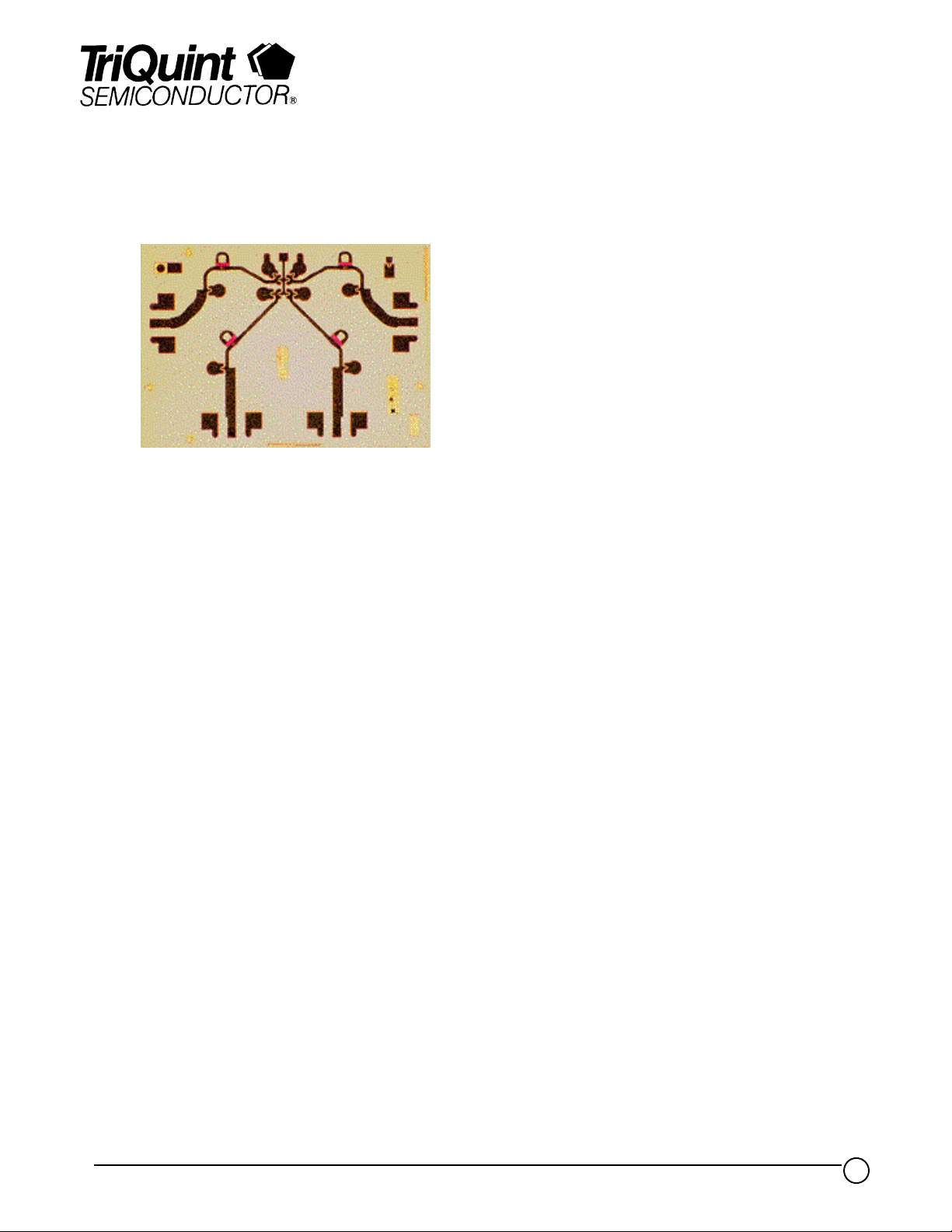
DC- 20 GHz SP4T PIN Switch TGS2304-SCC
Key Features and Performance
• DC to 20 GHz Frequency Range
• 0.6 dB Typical Midband Insertion Loss
• 38 dB Typical Midband Isolation
• Typical Input / Output SWR 1.2:1,
Midband
• 23 dB Typical Input Power at 1 dB Gain
Compression
• 2.540 x 3.556 x 0.1016 mm (0.100 x
0.140 x 0.004 in.)
Description
The TriQuint TGS2304-SCC is a GaAs monolithic PIN-diode single-pole, four-throw
switch, in chip form, that operates from DC to 20 GHz. Each arm consists of one
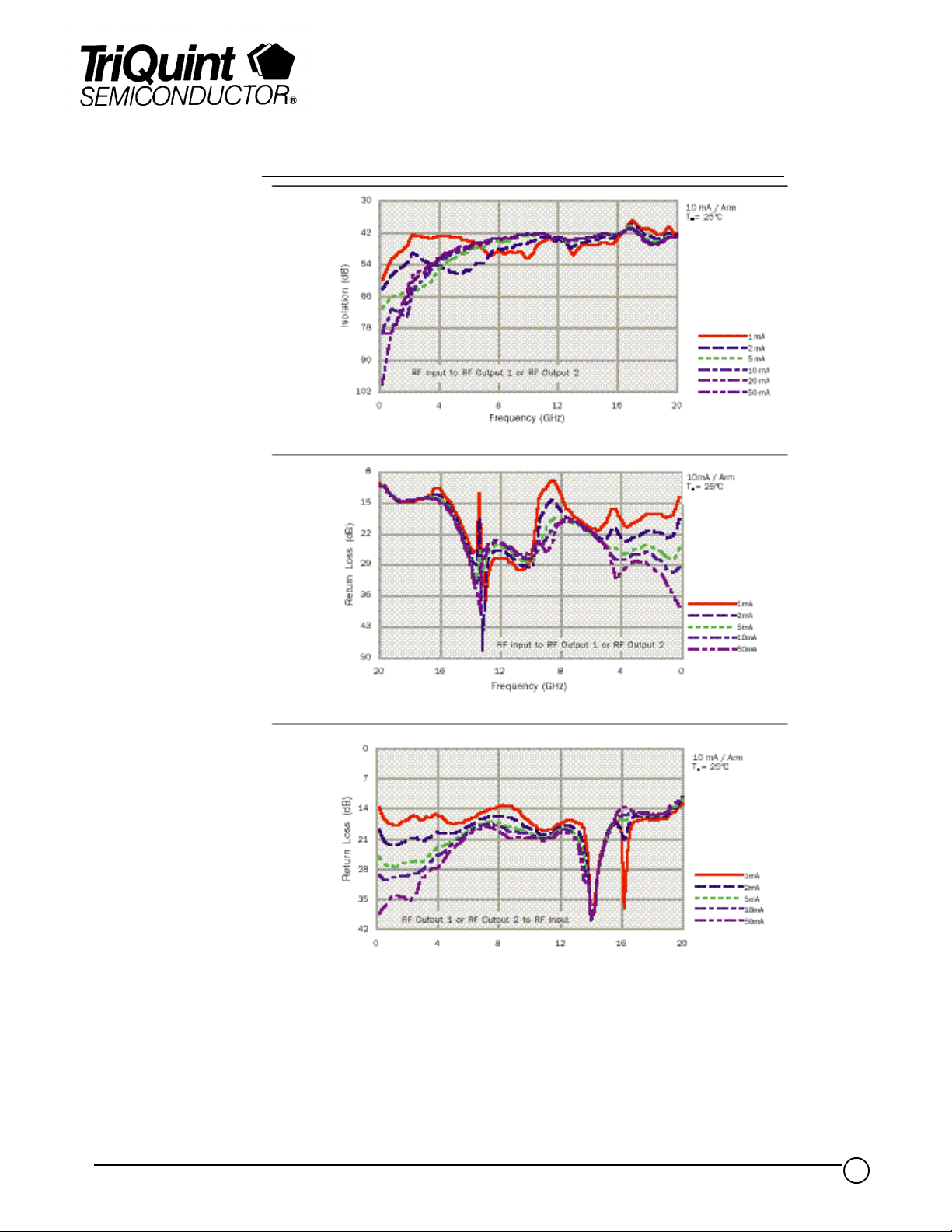
series and two shunt PIN diodes. At a bias current of 10 mA per RF output arm,
typical midband insertion loss is 0.6 dB; midband return loss is approximately 20
dB. Typical isolation at 10 mA bias is 40 dB. Insertion loss and isolation can be
adjusted by varying the switch arm bias currents.
Using a GaAs vertical PIN diode process, TriQuint has produced switches with high
power handling capability, low on-state resistance, and low off-state capacitance.
The higher cutoff frequency of the PIN diode element makes this switch ideal for
broadband electronic components and communication systems wherein the MMIC
construction offers reduced size, cost, and assembly time. Bond pad and backside
metallization is gold plated for compatibility with eutectic alloy attach methods as
well as thermocompression and thermosonic wire-bonding processes.
TriQuint Semiconductor Texas Phone: (972)994 8465 Fax: (972)994 8504 Web: www.triquint.com
1
Page 2
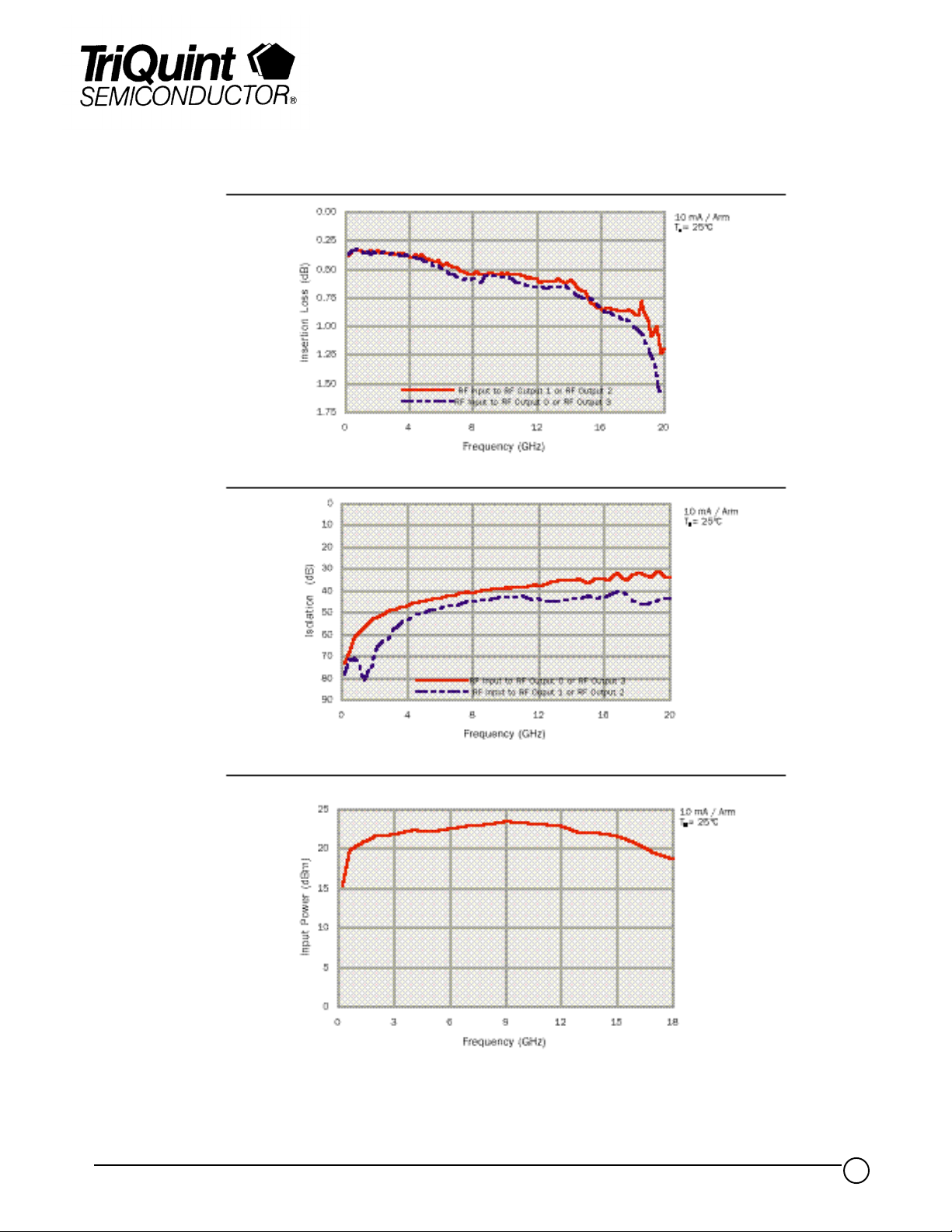
TYPICAL
INSERTION
LOSS
Product Data Sheet
TGS2304-SCC
TYPICAL
ISOLATION
TYPICAL
INPUT POWER
P
1dB
TriQuint Semiconductor Texas Phone: (972)994 8465 Fax: (972)994 8504 Web: www.triquint.com
2
Page 3
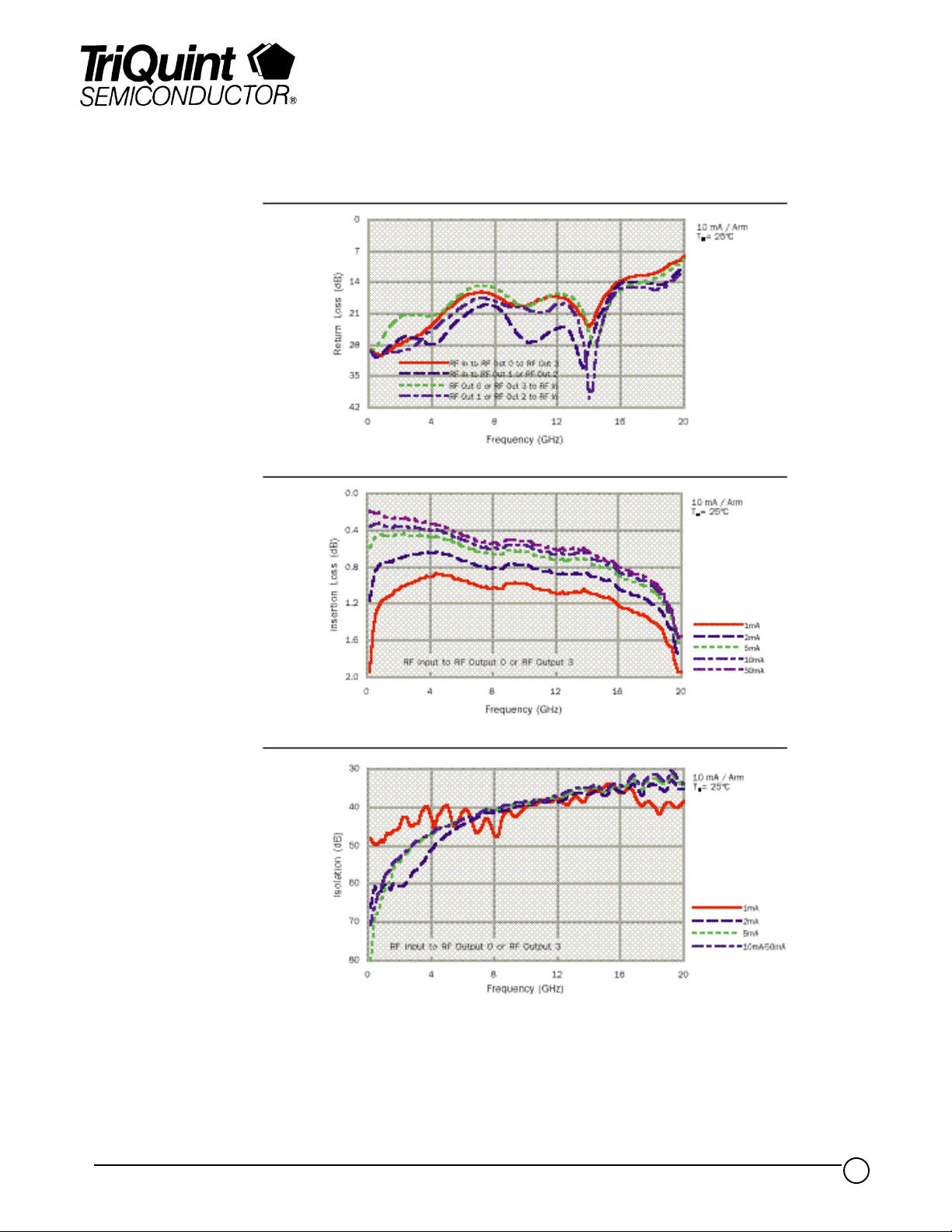
TYPICAL
RETURN LOSS
TYPICAL
INSERTION
LOSS VS. CONTROL
BIAS CURRENT
Product Data Sheet
TGS2304-SCC
TYPICAL ISOLATION
VS. CONTROL
BIAS CURRENT
TriQuint Semiconductor Texas Phone: (972)994 8465 Fax: (972)994 8504 Web: www.triquint.com
3
Page 4
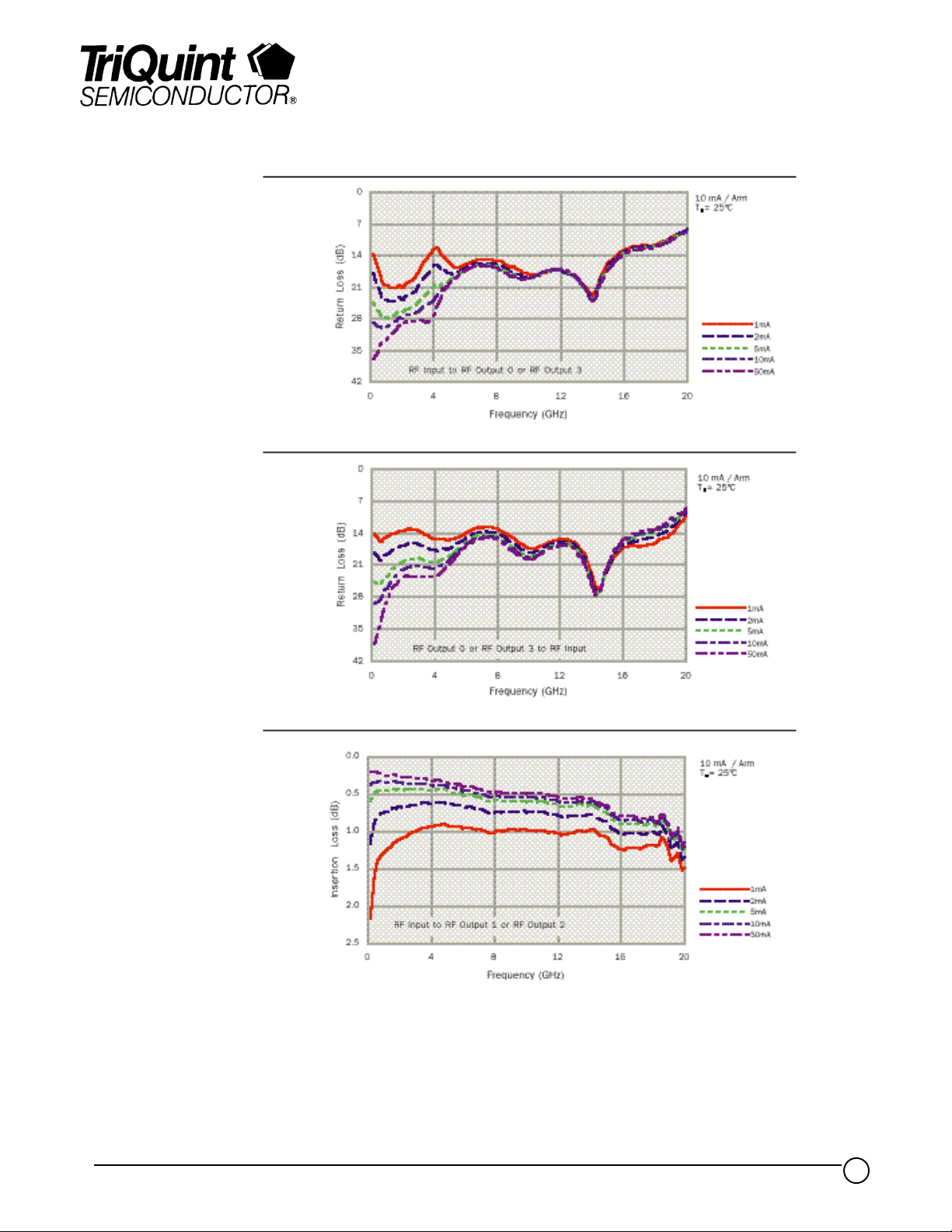
TYPICAL INPUT
RETURN LOSS VS.
CONTROL BIAS
CURRENT
TYPICAL OUTPUT
RETURN LOSS VS.
CONTROL BIAS
CURRENT
Product Data Sheet
TGS2304-SCC
TYPICAL INSERTION
LOSS VS. CONTROL
BIAS CURRENT
TriQuint Semiconductor Texas Phone: (972)994 8465 Fax: (972)994 8504 Web: www.triquint.com
4
Page 5
TYPICAL
ISOLATION VS.
CONTROL BIAS
CURRENT
TYPICAL
INPUT RETURN
LOSS VS. CONTROL
BIAS CURRENT
Product Data Sheet
TGS2304-SCC
TYPICAL
INPUT RETURN
LOSS VS. CONTROL
BIAS CURRENT
TriQuint Semiconductor Texas Phone: (972)994 8465 Fax: (972)994 8504 Web: www.triquint.com
5
Page 6

Product Data Sheet
.
…
TGS2304-SCC
ABSOLUTE
MAXIMUM
RATINGS
Forw ard Voltage, VF…………………………………………………………………………………………. 2.5 V
Forw ard Voltage, V
…………………………………………………………………………………………
R
30 V
Bias current…………………………………………………………………………………………………… 50 mA
Input c ontinuous w ave pow er, P
Mounting temperature (30 sec.), T
Storage temperature range, T
Ratings over oper ating channel temperature range, T
…………………………………………………………………………
IN
………………………………………………………………………….320oC
M
…………………………………………………………………………….-65 to 175oC
STG
(unless otherw ise noted).
CH
2 W
Stresses beyond those listed under "Absolute Maximum Ratings" may caus e per manent damage to the device.
These are stres s ratings only, and f unctional operation of the device at these or any other c onditions beyond
those indicated under "rec ommended operating conditions" is not implied. Expos ure to absolute maximum rated
conditions for extended periods may affect device reliability.
DC blocks are not provided at RF ports.
The operating junction temperature (T
) w ill directly affect the device MTTF. For maximum life, it is recommended
J
that junction temperature be maintained at the low est possible level.
TriQuint Semiconductor Texas Phone: (972)994 8465 Fax: (972)994 8504 Web: www.triquint.com
6
Page 7

Product Data Sheet
TGS2304-SCC
TYPICAL
S-PARAMETERS
(through path)
RF Input to RF output 3, 0
Freque ncy
S
11
(GHz) MAG ANG(°) MAG ANG(°) MAG ANG(°) MAG ANG(°) (dB)
S
21
S
12
S
22
Insertion Loss
0.5 0.03 -36 0.962 -6 0.960 -6 0.04 -45 0.3
1.0 0.03 -63 0.963 -11 0.963 -11 0.05 -59 0.3
1.5 0.04 90 0.959 -17 0.961 -17 0.07 -65 0.4
2.0 0.04 -106 0.959 -23 0.959 -23 0.08 -69 0.4
2.5 0.05 -117 0.961 -28 0.958 -28 0.09 -74 0.3
3.0 0.05 -117 0.960 -34 0.959 -34 0.09 -82 0.4
3.5 0.06 -114 0.957 -40 0.957 -40 0.09 -94 0.4
4.0 0.07 -111 0.955 -46 0.954 -45 0.08 -110 0.4
4.5 0.08 -112 0.955 -51 0.953 -51 0.09 -129 0.4
5.0 0.10 -117 0.951 -57 0.951 -57 0.11 -143 0.4
5.5 0.12 -126 0.948 -63 0.948 -63 0.13 -152 0.5
6.0 0.14 -136 0.945 -69 0.946 -69 0.15 -159 0.5
6.5 0.15 -146 0.940 -75 0.941 -74 0.17 -164 0.5
7.0 0.15 -154 0.937 -80 0.937 -80 0.18 -167 0.6
7.5 0.15 -163 0.935 -86 0.933 -86 0.18 -171 0.6
8.0 0.15 -169 0.935 -91 0.932 -91 0.18 -175 0.6
8.5 0.13 -171 0.932 -97 0.933 -97 0.16 177 0.6
9.0 0.12 -166 0.938 -102 0.939 -102 0.14 169 0.6
9.5 0.11 -162 0.937 -108 0.936 -108 0.12 157 0.6
10.0 0.11 -158 0.937 -114 0.936 -114 0.11 142 0.6
10.5 0.12 -161 0.935 -120 0.933 -120 0.11 130 0.6
11.0 0.13 -167 0.932 -126 0.931 -126 0.13 120 0.6
11.5 0.14 -175 0.930 -132 0.929 -132 0.14 112 0.6
12.0 0.14 176 0.927 -138 0.924 -138 0.15 108 0.7
12.5 0.13 165 0.927 -144 0.926 -144 0.15 106 0.7
13.0 0.11 158 0.927 -150 0.926 -150 0.13 103 0.7
13.5 0.09 160 0.927 -156 0.926 -156 0.10 96 0.7
14.0 0.06 -171 0.926 -163 0.925 -163 0.06 75 0.7
14.5 0.10 -133 0.920 -169 0.919 -169 0.04 -4 0.7
15.0 0.15 -129 0.917 -175 0.915 -175 0.09 -44 0.8
15.5 0.18 -131 0.916 179 0.913 179 0.13 -57 0.8
16.0 0.21 -137 0.909 172 0.908 172 0.16 -63 0.8
16.5 0.23 -145 0.904 166 0.902 166 0.18 -68 0.9
17.0 0.24 -152 0.900 159 0.899 159 0.19 -72 0.9
17.5 0.24 -159 0.897 152 0.896 152 0.20 -77 0.9
18.0 0.25 -166 0.893 145 0.892 145 0.21 -87 1.0
18.5 0.27 -165 0.887 137 0.885 138 0.23 -104 1.0
19.0 0.31 -161 0.871 130 0.872 130 0.27 -124 1.2
19.5 0.34 -154 0.854 122 0.845 123 0.31 -143 1.4
20.0 0.39 -156 0.833 118 0.839 119 0.36 -156 1.6
TA = 25OC, I = 10 mA
The reference planes for S-parameter data include bond wires as specified in the test assembly diagram.
The S-parameters are also available on floppy disk and the world wide web.
TriQuint Semiconductor Texas Phone: (972)994 8465 Fax: (972)994 8504 Web: www.triquint.com
7
Page 8

Product Data Sheet
TGS2304-SCC
TYPICAL
S-PARAMETERS
(isolated path)
RF Input to RF output 3
Freque ncy
S
11
(GHz) MAG ANG(°) MAG ANG(°) MAG ANG(°) M AG ANG(°) (dB)
S
21
S
12
S
22
0.5 0.06 15 0.0005 -87 0.0005 -75 0.90 177 66.3
1.0 0.06 -2 0.0011 -113 0.0011 -119 0.90 173 59.2
1.5 0.05 -22 0.0017 -132 0.0017 -129 0.88 169 55.2
2.0 0.04 -5 0.0023 -151 0.0023 -149 0.87 166 52.8
2.5 0.06 -52 0.0029 -160 0.0029 -162 0.87 163 50.8
3.0 0.02 -34 0.0037 -168 0.0037 -170 0.86 158 48.6
3.5 0.08 -57 0.0041 -180 0.0041 -180 0.87 153 47.7
4.0 0.07 -103 0.0046 175 0.0046 175 0.87 148 46.7
4.5 0.05 -95 0.0054 167 0.0054 168 0.88 144 45.4
5.0 0.08 -112 0.0058 163 0.0058 161 0.88 141 44.7
5.5 0.08 -131 0.0064 158 0.0064 157 0.88 138 43.9
6.0 0.07 -149 0.0070 154 0.0070 155 0.89 136 43.1
6.5 0.12 -140 0.0076 151 0.0076 150 0.88 133 42.4
7.0 0.13 173 0.0082 151 0.0082 150 0.88 129 41.7
7.5 0.05 -169 0.0095 143 0.0095 142 0.88 126 40.4
8.0 0.11 177 0.0092 140 0.0092 141 0.88 123 40.7
8.5 0.04 170 0.0103 138 0.0103 138 0.87 119 39.7
9.0 0.06 -153 0.0109 135 0.0109 135 0.87 114 39.3
9.5 0.08 -141 0.0115 130 0.0115 130 0.87 111 38.8
10.0 0.09 -164 0.0120 126 0.0120 126 0.87 107 38.4
10.5 0.10 -171 0.0123 127 0.0123 128 0.87 102 38.2
11.0 0.14 165 0.0123 124 0.0123 124 0.87 96 38.2
11.5 0.12 97 0.0134 126 0.0134 126 0.87 90 37.5
12.0 0.10 141 0.0132 123 0.0132 122 0.87 86 37.6
12.5 0.13 69 0.0153 125 0.0153 125 0.87 84 36.3
13.0 0.09 32 0.0167 120 0.0167 121 0.88 83 35.6
13.5 0.09 -42 0.0179 113 0.0179 113 0.87 82 34.9
14.0 0.09 -84 0.0178 109 0.0178 109 0.86 78 35.0
14.5 0.18 -78 0.0188 104 0.0188 102 0.86 73 34.5
15.0 0.22 -148 0.0159 102 0.0159 102 0.85 67 36.0
15.5 0.07 -79 0.0197 103 0.0197 104 0.86 62 34.1
16.0 0.22 -128 0.0188 95 0.0188 95 0.85 56 34.5
16.5 0.08 76 0.0220 101 0.0220 102 0.85 52 33.2
17.0 0.28 -97 0.0229 76 0.0229 76 0.85 48 32.8
17.5 0.08 -140 0.0197 89 0.0197 89 0.85 46 34.1
18.0 0.24 -90 0.0257 77 0.0257 77 0.86 43 31.8
18.5 0.40 -133 0.0238 61 0.0238 62 0.86 39 32.5
19.0 0.16 -156 0.0232 71 0.0232 72 0.85 31 32.7
19.5 0.51 -141 0.0247 44 0.0247 46 0.86 23 32.2
20.0 0.43 -164 0.0201 48 0.0201 48 0.83 18 33.9
Is o l a t i o n
TA = 25OC, I = 10 mA
The reference planes for S-parameter data include bond wires as specified in the test assembly diagram.
The S-parameters are also available on floppy disk and the world wide web.
TriQuint Semiconductor Texas Phone: (972)994 8465 Fax: (972)994 8504 Web: www.triquint.com
8
Page 9

Product Data Sheet
TGS2304-SCC
TYPICAL
S-PARAMETERS
(through path)
RF Input to RF output 2, 1
Freque ncy
S
11
(GHz) MAG ANG(°) MAG ANG(°) MAG ANG(°) M AG ANG(°) (dB)
S
21
S
12
S
22
Insertion Loss
0.5 0.03 -26 0.962 -6 0.964 -6 0.03 -33 0.3
1.0 0.03 -41 0.962 -12 0.963 -12 0.03 -49 0.3
1.5 0.04 -51 0.962 -18 0.963 -18 0.03 -61 0.3
2.0 0.05 -56 0.962 -24 0.962 -24 0.03 -72 0.3
2.5 0.05 -62 0.960 -29 0.960 -30 0.04 -81 0.4
3.0 0.05 -67 0.960 -35 0.959 -35 0.04 -86 0.4
3.5 0.04 -76 0.960 -41 0.957 -41 0.05 -91 0.4
4.0 0.04 -91 0.957 -48 0.957 -47 0.06 -99 0.4
4.5 0.04 -107 0.958 -53 0.956 -53 0.07 -109 0.4
5.0 0.06 -123 0.954 -59 0.954 -59 0.08 -123 0.4
5.5 0.07 -133 0.952 -65 0.952 -65 0.09 -136 0.4
6.0 0.08 -142 0.948 -71 0.951 -71 0.11 -147 0.5
6.5 0.10 -150 0.949 -77 0.945 -77 0.12 -157 0.5
7.0 0.11 -154 0.946 -83 0.946 -83 0.13 -166 0.5
7.5 0.11 -155 0.941 -89 0.944 -89 0.13 -176 0.5
8.0 0.11 -158 0.940 -95 0.940 -95 0.13 176 0.5
8.5 0.09 -164 0.940 -101 0.940 -101 0.12 172 0.5
9.0 0.07 -175 0.941 -106 0.940 -106 0.11 178 0.5
9.5 0.05 162 0.940 -112 0.939 -112 0.11 -176 0.5
10.0 0.04 144 0.939 -118 0.937 -118 0.10 -175 0.5
10.5 0.04 143 0.939 -124 0.940 -124 0.10 178 0.5
11.0 0.05 146 0.940 -130 0.938 -130 0.09 165 0.5
11.5 0.06 133 0.936 -136 0.939 -137 0.10 156 0.6
12.0 0.06 110 0.935 -143 0.935 -143 0.11 155 0.6
12.5 0.06 95 0.933 -149 0.933 -149 0.11 152 0.6
13.0 0.05 92 0.933 -155 0.932 -155 0.10 145 0.6
13.5 0.02 139 0.934 -161 0.932 -161 0.05 128 0.6
14.0 0.04 -143 0.933 -167 0.932 -167 0.01 66 0.6
14.5 0.07 -113 0.928 -174 0.931 -174 0.04 -84 0.6
15.0 0.11 -93 0.924 180 0.921 180 0.09 -111 0.7
15.5 0.16 -90 0.912 174 0.914 174 0.14 -123 0.8
16.0 0.19 -94 0.908 168 0.907 168 0.17 -130 0.8
16.5 0.20 -103 0.908 161 0.907 161 0.18 -129 0.8
17.0 0.21 -108 0.907 154 0.908 155 0.18 -133 0.8
17.5 0.20 -113 0.905 148 0.907 148 0.18 -138 0.9
18.0 0.20 -122 0.906 141 0.907 141 0.17 -143 0.9
18.5 0.19 -142 0.909 135 0.904 134 0.17 -133 0.8
19.0 0.21 -167 0.896 127 0.900 127 0.19 -125 1.0
19.5 0.25 -178 0.891 120 0.883 120 0.22 -130 1.0
20.0 0.30 -174 0.871 113 0.882 114 0.26 -151 1.2
T
= 25OC, I = 10 mA
A
The reference planes for S-parameter data include bond wires as specified in the test assembly diagram.
The S-parameters are also available on floppy disk and the world wide web.
TriQuint Semiconductor Texas Phone: (972)994 8465 Fax: (972)994 8504 Web: www.triquint.com
9
Page 10

Product Data Sheet
TGS2304-SCC
TYPICAL
S-PARAMETERS
(isolated path)
RF Input to RF output 2, 1
Freque ncy
S
11
(GHz) MAG ANG(°) MAG ANG(°) MAG ANG(°) MAG ANG(°) (dB)
S
21
S
12
S
22
0.5 0.06 10 0.0003 127 0.0003 59 0.90 177 70.3
1.0 0.06 -35 0.0002 98 0.0002 48 0.90 173 74.0
1.5 0.08 -69 0.0001 -70 0.0001 -112 0.89 169 79.3
2.0 0.07 -80 0.0004 147 0.0004 159 0.88 165 68.0
2.5 0.12 -88 0.0007 156 0.0007 161 0.87 162 63.1
3.0 0.06 -102 0.0011 163 0.0011 161 0.87 158 59.2
3.5 0.09 -77 0.0017 155 0.0017 149 0.87 155 55.4
4.0 0.09 -106 0.0022 145 0.0022 140 0.87 151 53.2
4.5 0.07 -102 0.0029 138 0.0029 139 0.88 147 50.9
5.0 0.11 -117 0.0032 130 0.0032 130 0.88 143 49.9
5.5 0.13 -135 0.0036 124 0.0036 123 0.88 140 48.8
6.0 0.12 -150 0.0040 120 0.0040 120 0.89 137 48.0
6.5 0.16 -141 0.0048 115 0.0048 113 0.89 134 46.4
7.0 0.18 -172 0.0047 108 0.0047 110 0.89 132 46.6
7.5 0.12 -155 0.0059 109 0.0059 108 0.89 128 44.6
8.0 0.19 -169 0.0059 93 0.0059 94 0.88 124 44.6
8.5 0.10 -177 0.0061 91 0.0061 91 0.89 121 44.3
9.0 0.10 -156 0.0062 90 0.0062 90 0.88 118 44.2
9.5 0.10 -139 0.0072 86 0.0072 85 0.88 115 42.9
10.0 0.12 -148 0.0075 77 0.0075 76 0.88 111 42.5
10.5 0.15 -150 0.0073 70 0.0073 70 0.87 107 42.7
11.0 0.21 -170 0.0076 59 0.0076 61 0.88 103 42.4
11.5 0.14 151 0.0066 47 0.0066 48 0.88 101 43.6
12.0 0.18 172 0.0067 51 0.0067 53 0.89 100 43.5
12.5 0.13 122 0.0059 44 0.0059 44 0.88 98 44.5
13.0 0.07 115 0.0057 44 0.0057 44 0.89 94 44.9
13.5 0.03 -134 0.0061 43 0.0061 43 0.87 88 44.3
14.0 0.11 -145 0.0065 38 0.0065 39 0.88 81 43.7
14.5 0.15 -112 0.0066 35 0.0066 34 0.87 76 43.6
15.0 0.31 -152 0.0077 28 0.0077 27 0.87 72 42.3
15.5 0.12 -153 0.0070 20 0.0070 20 0.85 71 43.1
16.0 0.28 -141 0.0075 22 0.0075 22 0.87 66 42.5
16.5 0.17 139 0.0086 14 0.0086 13 0.85 64 41.3
17.0 0.26 -108 0.0102 -5 0.0102 -5 0.87 62 39.8
17.5 0.18 -178 0.0073 -25 0.0073 -24 0.87 63 42.7
18.0 0.20 -110 0.0057 -22 0.0057 -24 0.87 59 44.9
18.5 0.39 -143 0.0050 -20 0.0050 -18 0.88 52 46.1
19.0 0.27 173 0.0055 -14 0.0055 -16 0.86 39 45.2
19.5 0.55 -160 0.0065 -23 0.0065 -27 0.89 29 43.7
20.0 0.55 178 0.0070 -28 0.0070 -29 0.85 27 43.1
Is o la t i o n
TA = 25OC, I = 10 mA
The reference planes for S-parameter data include bond wires as specified in the test assembly diagram.
The S-parameters are also available on floppy disk and the world wide web.
TriQuint Semiconductor Texas Phone: (972)994 8465 Fax: (972)994 8504 Web: www.triquint.com
10
Page 11

Product Data Sheet
TGS2304-SCC
RF CHARACTERISTICS
EQUIVALENT
SCHEMATIC
PARA METER TEST CONDITIONS TY P
IL Insertion loss Midband 0.6
ISO Is olation Midband 38
SWR(in) Input standing–w ave ratio Midband 1.2:1
SWR(out) Output standing–w ave ratio Through selected output arm, midband 1.2:1
P
1dB(in)
Input pow er at 1–dB gain compression 23
TA = 25OC
RECOMMENDED TEST
CONFIGURATION
TriQuint Semiconductor Texas Phone: (972)994 8465 Fax: (972)994 8504 Web: www.triquint.com
11
Page 12

Product Data Sheet
TGS2304-SCC
FUNCTION TABLE
TEST ASSEMBLY
DIAGRAM
LOW–LOSS PATH RF INPUT RF OUTPUT 0 RF OUTPUT 1 RF OUTP UT 2 RF OUTP UT 3
RF Input to RF Output 0 0 V -10 mA 10 mA 10 mA 10 mA
RF Input to RF Output 1 0 V 10 mA -10 mA 10 mA 10 mA
RF Input to RF Output 2 0 V 10 mA 10 mA -10 mA 10 mA
RF Input to RF Output 3 0 V 10 mA 10 mA 10 mA -10 mA
RF connections: bond using three 1.0-mil diameter, 20 to 25-mil-length gold bond wires at both RF Input and RF
Output for optimum RF performance.
Close placement of external components is essential for resonant-free performance.
Refer to TriQuint’s Gallium Arsenide Products Designer’s Information, MMIC Assembly Procedures, on our
web site.
TriQuint Semiconductor Texas Phone: (972)994 8465 Fax: (972)994 8504 Web: www.triquint.com
12
Page 13

MECHANICAL
DRAWING
Product Data Sheet
TGS2304-SCC
TriQuint Semiconductor Texas Phone: (972)994 8465 Fax: (972)994 8504 Web: www.triquint.com
13
Page 14

Product Data Sheet
TGS2304-SCC
Driver Circuit for 2300 Series GaAs PIN Diode SwitchesApplication Notes:
INTRODUCTION
CONNECTION
INSTRUCTIONS
This section describes how a single 5 V power supply and a 74F24ON line driver
are used in a driver circuit for the TGS2304 PIN-diode switch. The PIN switch
must be mounted on a silicon MOS capacitor (MOSCAP or equivalent) of
approximately 1000 pF (see Mounting Diagram, page 15). Eight separate drivers
are provided in a single ‘F240 DIP (see Driver Circuit, page 15). In addition, the
‘F240 can be set to provide an inverted or a non-inverted output. The inverted is
preferred in this application because it allows the 1G pin to be tied to ground
instead of 5 V, eliminating the use of an extra power supply. The 74BCT240,
74BCT240N, and 74S240N also work with this driver circuit.
The Interface Schematic (see page 16) shows a voltage divider that can be used
to provide approximately 2 V to the RF Input (common) port of the TGS2304-SCC.
This bias voltage should be connected to the RF Input through a bias tee or some
equivalent RF choke/DC block network.
Connect this same bias voltage to the top plate of the MOSCAP through a ~3-nH
coil bonded to MMIC ground pad as shown in the Interface Schematic and RF
Input Bias Coil Assembly (both on page 16). Care should be taken not to bond the
inductor close to the via, as this could result in device damage. The ground pad is
connected to the backside of the TGS2304-SCC by plated-through vias. This sets
the top plate of the MOSCAP to 2 V, effectively providing a 2 V reference for the
RF input port and the cathodes of the two shunt diodes in each arm. The bottom
plate of the MOSCAP is true DC ground.
OPERATING
INSTRUCTIONS
TriQuint Semiconductor Texas Phone: (972)994 8465 Fax: (972)994 8504 Web: www.triquint.com
Connect the four RF Output ports of the TGS2304-SCC to the ‘F240 outputs
through a bias tee or some equivalent RF choke/DC block, as shown in the
Interface Schematic on page 16.
For proper switch operation, only one arm should be turned on at any one time as
shown in the Control Logic Table on page 15. The following description of how the
driver circuit controls one arm of the TGS2304-SCC applies to all arms.
To turn an arm on: A TTL high at the ‘F240 input results in approximately 0.3 V at
the corresponding output. This is applied to the appropriate RF Output port. Since
the RF Input port of the TGS2304-SCC is at 2 V, the arm is turned on. The series
diode in that arm is forward biased by approximately 1.7 V, and the two shunt
diodes are reverse biased (off) by 1.7 V. Under these conditions, the bias current
is typically 12 mA and midband insertion loss is typically 0.9 dB.
To turn an arm off: A TTL low at the ‘F240 input results in approximately 3.1 V at
the corresponding output. This is applied to the appropriate RF Output port. Since
the RF Input port of the TGS2304-SCC is at 2 V, the arm is turned off. The series
diode in that arm is reverse biased by approximately 1.1 V, and the shunt diodes
in that arm are forward biased (on) by 1.1 V. Under these conditions, the bias
current is typically 9 mA and the midband isolation is typically 40 dB.
14
Page 15

Product Data Sheet
F
TGS2304-SCC
CONTROL LOGIC
TABLE
MOUNTING DIAGRAM
DRIVER VOLTAGE AP P LIED AT R
01230123
L H H H ON OFF OFF OFF
TGS2304–SCC H L H H OFF ON OFF OFF
H H L H OFF OFF ON OFF
H H H L OFF OFF OFF ON
L = low (typically 0.3 V), H = high (typically 3.1 V)
RF SWITCH ARMS
DRIVER CIRCUIT
TriQuint Semiconductor Texas Phone: (972)994 8465 Fax: (972)994 8504 Web: www.triquint.com
15
Page 16

INTERFACE
SCHEMATIC
Product Data Sheet
TGS2304-SCC
RF INPUT BIAS
COIL ASSEMBLY
GaAs MMIC devices are susceptible to damage from Electrostatic Discharge. Proper precautions should be observed
during handling, assembly and test.
TriQuint Semiconductor Texas Phone: (972)994 8465 Fax: (972)994 8504 Web: www.triquint.com
16
 Loading...