

Page 1
Product Data Sheet
6 - 18 GHz Phase Shifter TGP6336-EEU
Key Features and Performance
• 6 to 18 GHz Frequency Range
• 5-Bit Phase Shifter
• On-Chip CMOS-Compatible Drivers
• 9 dB Typical Insertion Loss at Midband
• 2:1 Typical Input SWR: 2.6:1 Typical
Output SWR
• 3.556 x 2.540 x 0.1016 mm (0.140 x
0.100 x 0.004 in.)
Description
The TriQuint TGP6336-EEU is a GaAs MMIC 5-bit phase shifter which operates
from 6 to 18 GHz. Phase can be shifted from 0 to 348.75 degrees in 11.25 degree
steps. Control bias voltages are 0 and 5 V. The insertion loss is typically 9 dB.
The TGP6336-EEU features on-chip CMOS-compatible drivers. The FET based
phase shifter offers wide band performance and small size for use in T/R modules
for EW applications.
Bond pad and backside metallization is gold plated for compatibility with eutectic
alloy attach methods as well as thermocompression and thermosonic wire-bonding
processes. Ground is provided to the circuitry through vias to the backside
metallization.
TriQuint Semiconductor Texas Phone: (972)994 8465 Fax: (972)994 8504 Web: www.triquint.com
1
Page 2
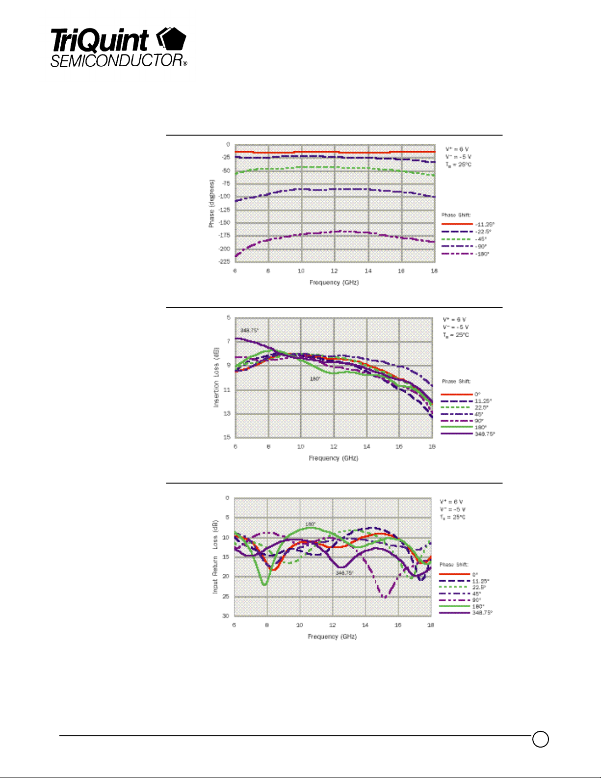
TYPICAL
RELATIVE
PHASE
TYPICAL
INSERTION
LOSS
Product Data Sheet
TGP6336-EEU
TYPICAL
INPUT
RETURN LOSS
TriQuint Semiconductor Texas Phone: (972)994 8465 Fax: (972)994 8504 Web: www.triquint.com
2
Page 3
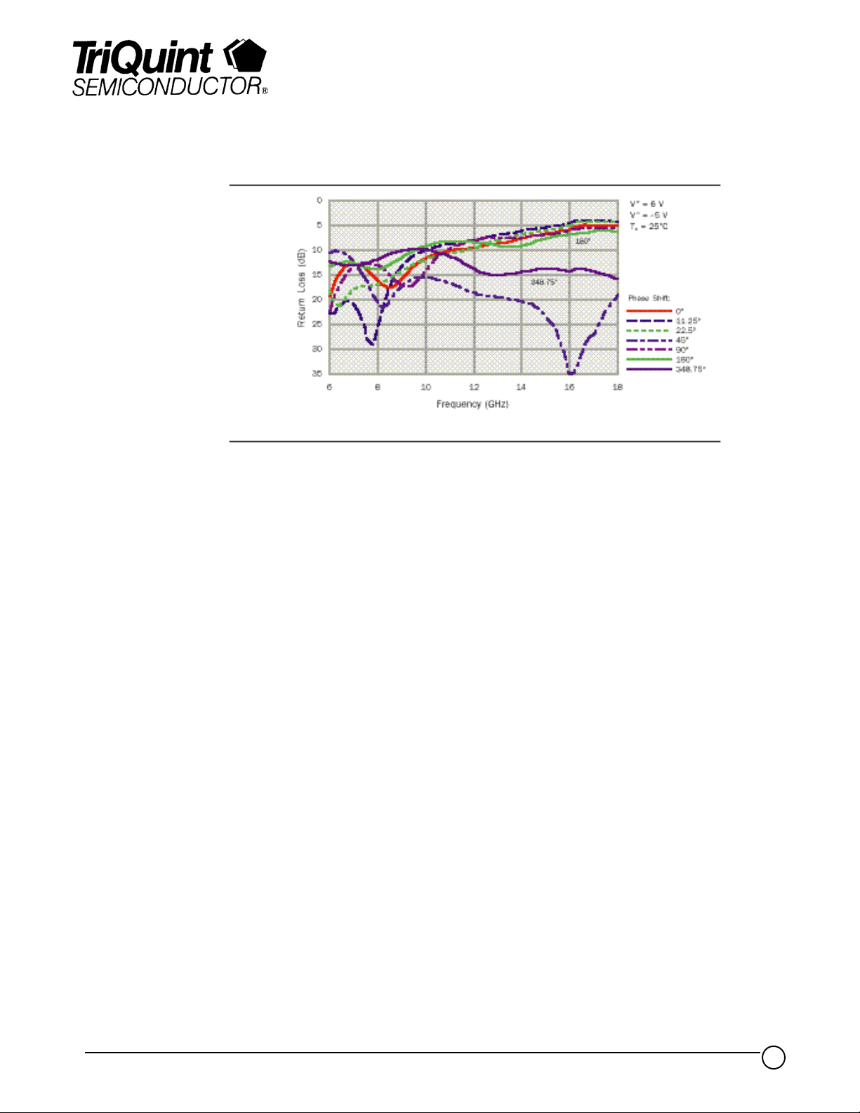
TYPICAL OUTPUT
.
.
…
RETURN LOSS
Product Data Sheet
TGP6336-EEU
ABSOLUTE
MAXIMUM
RATINGS
Positive supply voltage, V+………………………………………………………………………………….. 8 V
Positive supply voltage range w ith respect to negative supply voltage, V+ - V-………………………
Negative supply voltage range, V-………………………………………………………………………….
Input c ontinuous w ave pow er, P
…………………………………………………………………………
IN
0 V to 12 V
0 V to -6 V
1 W
Control voltage range, SHF 90, SHF180, SHF11.25, SHF 22.5, SHF 45……………………………….. 0 V to V+
Operating Channel temperature, T
Mounting temperature (30 sec.), T
Storage temperature range, T
Ratings over oper ating channel temperature range, T
*.………………………………………………………………………150oC
CH
………………………………………………………………………….320oC
M
…………………………………………………………………………….-65 to 150oC
STG
(unless otherwise noted).
CH
Stresses beyond those listed under "Abs olute Maximum Ratings" may cause permanent damage to the device.
These are stress ratings only, and f unc tional operation of the devic e at thes e or any other conditions beyond
those indicated under "RF Charac teristic s" is not implied. Exposure to absolute maximum rated conditions
for extended periods may af f ect device reliability.
* Operating channel temperature (T
) w i l l dir e c tly af fec t t h e d e v i c e MTTF. Fo r max imum lif e, it is rec o mme nde d
CH
that channel temperature be maintained at the low est possible level.
TriQuint Semiconductor Texas Phone: (972)994 8465 Fax: (972)994 8504 Web: www.triquint.com
3
Page 4

Product Data Sheet
TGP6336-EEU
BIAS TRUTH TABLE
RELATIV E SHF 180 SHF 90 SHF 45 SHF 22.5 SHF 11.25
PHASE SHIFT (Bond pad #10)
(degrees)
0.00 5 5 5 5 5
-11.25 5 5 5 5 0
-22.50 5 5 5 0 5
-33.75 5 5 5 0 0
-45.00 5 5 0 5 5
-56.25 5 5 0 5 0
-67.50 5 5 0 0 5
-78.75 5 5 0 0 0
-90.00 5 0 5 5 5
-101.25 5 0 5 5 0
-112.50 5 0 5 0 5
-123.75 5 0 5 0 0
-135.00 5 0 0 5 5
-146.25 5 0 0 5 0
-157.50 5 0 0 0 5
-168.75 5 0 0 0 0
-180.00 0 5 5 5 5
-191.25 0 5 5 5 0
-202.50 0 5 5 0 5
-213.75 0 5 5 0 0
-225.00 0 5 0 5 5
-236.25 0 5 0 5 0
-247.50 0 5 0 0 5
-258.75 0 5 0 0 0
-270.00 0 0 5 5 5
-281.25 0 0 5 5 0
-292.50 0 0 5 0 5
-303.75 0 0 5 0 0
-315.00 0 0 0 5 5
-326.25 0 0 0 5 0
-337.50 0 0 0 0 5
-348.75 0 0 0 0 0
Bond pad #11 (Bond pad #7) (Bond pad #8) (Bond pad #9)
V+ = 6 V, V- = -5 V, TA = 25oC
TriQuint Semiconductor Texas Phone: (972)994 8465 Fax: (972)994 8504 Web: www.triquint.com
4
Page 5

Product Data Sheet
TGP6336-EEU
RF CHARACTERISTICS
RECOMMENDED BIAS
NETWORK
PARAMETER TEST CONDITIONS TYP UNIT
IL Insertion loss (all states) f = 6 - 18 GHz 9 dB
SWR(in) Input standing wave ratio f = 6 - 18 GHz (all states) 2.0:1 -
SWR(out) Output standing w ave ratio f = 6 - 18 GHz (all states) 2.6:1 -
P
(in)
1dB
PHASE TYPICAL RELATIVE PHASE SHIFT TYPICAL INPUT POWER at
(degrees) (degrees) (degrees) (degrees)
-348.75 -416±8 -326±9 380±11 25
Input pow er at 1–dB gain compression see next table
SHIFT at 6GHz at 12GHz at 18GHz 1–dB GAIN COMPRESSION at
MIDBA ND(d Bm)
-11.25 -13±2 -13.5±2 13±4 26
-22.5 -23±2 - 23±2 32±4 27
-45 -55±4 -43±3 58±7 26
-90 -107±5 -84±7 99±8 25
-180 -214±4 -165±8 186±16 25
V+ = 6 V, V- = -5 V, T
= 25oC
A
All bias resistors have a nominal value of 25-Ohms.
RF connections: Bond one 1-mil diameter, 20 to 25-mil-length gold bond wires at both RF Input and
RF Output for optimum RF performance.
Close placement of external components is essential for resonant-free performance.
Refer to TriQuint’s Gallium Arsenide Products Designers’ Information on our website under Application
Information.
TriQuint Semiconductor Texas Phone: (972)994 8465 Fax: (972)994 8504 Web: www.triquint.com
5
Page 6

FUNCTIONAL BLOCK
DIAGRAM
Product Data Sheet
TGP6336-EEU
TriQuint Semiconductor Texas Phone: (972)994 8465 Fax: (972)994 8504 Web: www.triquint.com
6
Page 7

MECHANICAL
DRAWING
Product Data Sheet
TGP6336-EEU
GaAs MMIC devices are susceptible to damage from Electrostatic Discharge. Proper precautions should be observed
during handling, assembly and test.
TriQuint Semiconductor Texas Phone: (972)994 8465 Fax: (972)994 8504 Web: www.triquint.com
7
 Loading...