

Page 1
T R I Q U I N T S E M I C O N D U C T O R , I N C .
TGL6425-SCC Digital Attenuator
6425
0.5 to 18-GHz Frequency Range
●
5- Bit Step Attenuator
●
15.5-dB Attenuation Range
●
4-dB Typical Inser tion Loss
●
1.6:1 Input/Output SWR
●
2,1844 x 1,8288 x 0,1016 mm (0.086 x 0.072 x 0.004 in.)
●
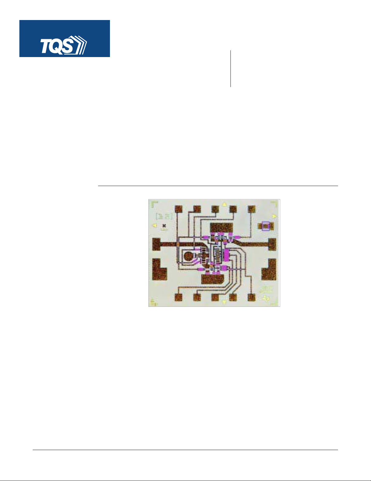
PHOTO ENLARGEMENT
DESCRIPTION
The TriQuint TGL6425-SCC is a GaAs MMIC 5-bit FET attenuator which operates fr om
0.5 to 18-GHz. The attenuation step is 0.5- dB and is controlled by 10 input lines. Control bias voltages
are 0 V and - 5 V. The input and output return loss is typically 13 -dB.
This unique absorptive design combines both “T”and “PI”configurations to produce an extremely
small size and low inser tion loss attenuator. The small size and reliability advantage of a monolithic
attenuator over a hybrid design make this device attractive for use in electronic war fare, radar,
telecommunication, and navigation systems for level set, modulation and switching functions.
Bond pad and backside metallization is gold plated for compatibility with eutectic alloy attachment
method as well as the thermocompression and thermosonic wire bonding processes. Ground is
provided to the circuitry through vias to the backside metallization.
TriQuint Semiconductor, Inc. • Texas Facilities • (972) 995-8465
• www.triquint.com
Page 2
TGL6425-SCC
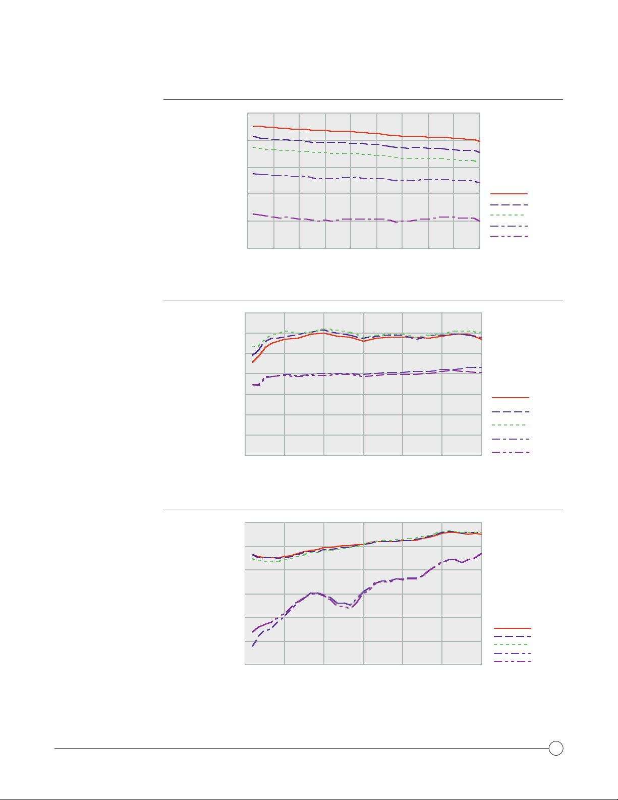
TYPICAL ATTENUATION
TYPICAL
INPUT POWER
P
1dB
0
-5
-10
-15
Attenuation (dB)
-20
-25
024681012141618
Frequency (GHz)
35
30
25
20
15
10
Input Power (dBm)
5
0
0369121518
Frequency (GHz )
TA= 25°C
Attenuation
State:
TA= 25°C
Attenuation
State:
0 dB
2 dB
4 dB
8 dB
15.5 dB
0 dB
2 dB
4 dB
8 dB
15.5 dB
TYPICAL
7
INPUT RETURN LOSS
13
19
25
31
Input Return Loss (dB)
37
43
0369121518
TriQuint Semiconductor, Inc. • Texas Facilities • (972) 995-8465
Frequency (GHz )
• www.triquint.com
T = 25°C
Attenuation
State:
0 dB
2 dB
4 dB
8 dB
15.5 dB
2
Page 3
TGL6425-SCC
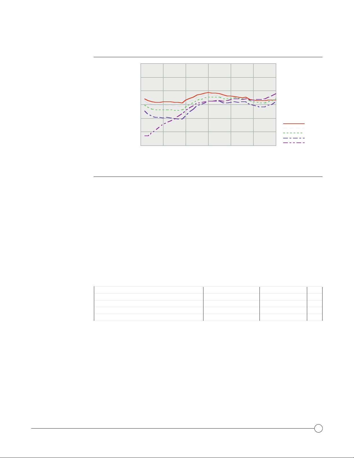
TYPICAL
OUTPUT RETURN LOSS
ABSOLUTE
MAXIMUM RATINGS
0
6
12
18
24
Output Return Loss (dB)
30
36
0369121518
TA= 25°C
Attenuation
State:
0dB
2dB
4dB
8dB
15.5dB
Frequency (GHz )
Input continuous wave power , P
.......................................................................................................... 1 W
IN
Control voltage range, V1, V2, V3, V4, V5, V6, V7, V8, V9, V10 ................................................-10 V to 0 V
Operating channel temperature, TCH* ................................................................................................ 150 °C
Mounting temperature (30 sec), TM .................................................................................................... 320°C
Storage temperature range, T
Ratings over operating channel temperature range, TCH(unless otherwise noted)
............................................................................................-65 to 150°C
STG
Stresses beyond those listed under “Absolute Maximum Ratings” may cause permanent damage to the device.
These are stress ratings only and functional operation of the device at these or any other conditions beyond
those indicated under “RF Characteristics” is not implied. Exposure to absolute maximum rated conditions for
extended periods may affect device reliability.
*Operating channel temperature, TCH, will directly affect the device MTTF . For maximum life, it is recommended
that channel temperature be maintained at the lowest possible level.
RF CHARACTERISTICS
PARAMETER TEST CONDITIONS TYPICAL UNIT
Attenuation see next table dB
SWR(in) Input standing wave ratio
SWR(out) Output standing wave ratio
P
(in) Input power at 1-dB gain compression see next table dBm
1dB
TriQuint Semiconductor, Inc. • Texas Facilities • (972) 995-8465
f = 2 - 18 GHz (all states) 1.6:1 -
f = 2 - 18 GHz (all states) 1.4:1 -
TA = 25°C
• www.triquint.com
3
Page 4

TGL6425-SCC
RF CHARACTERISTICS
BIAS TRUTH TABLE
ATTENUATION TYPICAL TYPICAL INPUT POWER
STATE
(dB)
TYPICAL
ATTENUATION
at 9 GHz (dB) at 9 GHz (dB) 2-18 GHz (dBm)
VARIANCE
1–dB Gain Compression
at
0 3.6 ± 0.25 28
0.5 4.1 ± 0.25 28
1 4.4 ± 0.25 29
2 5.7 ± 0.25 29
4 7.6 ± 0.25 29
8 12.1 ± 0.45 20
15.5 19.7 ± 0.7 20
ATTEN
STATE V
(dB)
1
V
2
V
3
V
4
V
5
V
6
V
7
V
8
V
9
V
10
0.0-50-5-5-50000-5
0.5-50-5-5-500000
1.0 -5 0 -5 -5 0 0 -5 -5 0 -5
1.5 -5 0 -5 -5 0 0 -5 -5 0 0
2.0-50-50-5-500-5-5
2.5-50-50-5-500-50
3.0 -5 0 -5 0 0 -5 0 -5 -5 -5
3.5 -5 0 -5 0 0 -5 0 -5 -5 0
4.0-500-5-5-5-5 0 0-5
4.5-500-5-5-5-5 0 00
5.0-500-50-5-50-5-5
5.5-500-50-5-50-50
6.0 -5 0 0 0 -5 -5 -5 -5 0 -5
6.5 -5 0 0 0 -5 -5 -5 -5 0 0
7.0-50000-5-5-5-5-5
7.5-50000-5-5-5-50
8.00-5-5-5-50000-5
8.50-5-5-5-500000
9.0 0 -5 -5 -5 0 0 -5 -5 0 -5
9.5 0 -5 -5 -5 0 0 -5 -5 0 0
10.0 0 -5 -5 0 -5 -5 0 0 -5 -5
10.5 0 -5 -5 0 -5 -5 0 0 -5 0
11.0 0 -5 -5 0 0 - 5 0 -5 -5 -5
11.5 0 -5 -5 0 0 - 5 0 -5 -5 0
12.0 0 -5 0 -5 -5 - 5 -5 0 0 -5
12.5 0 -5 0 -5 -5 - 5 -5 0 0 0
13.0 0 -5 0 -5 0 -5 - 5 0 -5 -5
13.5 0 -5 0 -5 0 -5 - 5 0 -5 0
14.0 0 -5 0 0 - 5 - 5 - 5 - 5 0 -5
14.5 0 -5 0 0 - 5 - 5 - 5 - 5 0 0
15.0 0 -5 0 0 0 -5 -5 -5 -5 -5
15.5 0 -5 0 0 0 -5 -5 -5 -5 0
TriQuint Semiconductor, Inc. • Texas Facilities • (972) 995-8465
• www.triquint.com
4
Page 5

TGL6425-SCC
EQUIVALENT
SCHEMATIC
BIAS NETWORK
RF
INPUT
100mm
2 - 290mm
V
V
2
1
2 - 32mm
2 - 62mm
V
3
RF Input
2 - 16mm
V
4
2 - 186mm
2 - 70mm
2 - 30mm
2 - 32mm
2 - 16mm
2 - 62mm
RF
OUTPUT
2 - 50mm
2 - 55mm
V
10
V5V
V9V
8
10
6
7
RF Output
V7V6V
5
V
V2V
1
3
3245
1
TGL6425
1112 10 9 8
V9V8V6V7V
4
All bias resistors have a nominal value of 25 - Ohms.
RF connections: Bond using two 1-mil diameter , 20 to 25-mil- length gold bond wires at both RF Input and
RF Output for optimum RF performance.
DC blocks are not provided at RF por ts.
Close placement of external components is essential to resonant-free performance.
TriQuint Semiconductor, Inc. • Texas Facilities • (972) 995-8465
• www.triquint.com
5
Page 6

MECHANICAL DRAWING
TGL6425-SCC
1,8288 (0.0720)
1,6358 (0.0644)
1,0592 (0.0417)
0,1880 (0.0074)
0.0
1
0.0
1,3970 (0.055)
23456
89101112
2,0396 (0.0803)
7
1,0592 (0.0417)
0,5029 (0.0198)
Units: Millimeters (inches)
Thickness: 0,102 (0.004) (reference only)
Chip edge to bond pad dimensions are shown to center of bond pad.
Chip size ±0,0508 (0.002)
Bond pad #1 (RF In): 0,127 x 0,207 (0.0050 x 0.0082) Bond pad #7 (RF Out): 0,246 x 0,119 (0.0097 x 0.0047)
Bond pad #2 (V
Bond pad #3 (V
Bond pad #4 (V
Bond pad #5 (V
Bond pad #6 (V
): 0,120 x 0,120 (0.0047 x 0.0047) Bond pad #8 (V4): 0,120 x 0,120 (0.0047 x 0.0047)
1
): 0,120 x 0,120 (0.0047 x 0.0047) Bond pad #9 (V7): 0,120 x 0,120 (0.0047 x 0.0047)
3
): 0,120 x 0,120 (0.0047 x 0.0047) Bond pad 1#0 (V6): 0,120 x 0,120 (0.0047 x 0.0047)
2
): 0,120 x 0,120 (0.0047 x 0.0047) Bond pad #11 (V8): 0,120 x 0,120 (0.0047 x 0.0047)
5
): 0,120 x 0,120 (0.0047 x 0.0047) Bond pad #12 (V9): 0,120 x 0,120 (0.0047 x 0.0047)
10
TriQuint Semiconductor, Inc. • Texas Facilities • (972) 995-8465
0,8077 (0.0318)
1,1049 (0.0435)
• www.triquint.com
1,3691 (0.0539)
1,7145 (0.0675)
2,1844 (0.0860)
6
Page 7

Application Notes: Suggested Driver Circuit
TGL6425-SCC
OVERVIEW
DRIVER CIRCUIT
SCHEMATIC
The following is a suggested driver circuit for the TriQuint TGL6425-SSC 0.5 to 18 - Ghz
step attenuator. The circuit allows the user to use a digital binary input to achieve the desired level
of attenuation; with a digital word of “00000” equaling0 -dB r elative attenuation and “11111”
equaling 15.5- dB relative attenuation. The JFET s (2N5116 or equivalent) provide the r equired level
shift from TTL voltages to attenuation control levels. The 2 - input NOR gates should be CMOS
(74C02 or equivalent) with 0 V applied to the positive supply terminal and -5 V on the negative
supply terminal.
~ 5k Ohms
TriQuint Semiconductor, Inc. • Texas Facilities • (972) 995-8465
• www.triquint.com
7
 Loading...