

Page 1
INTEGRATED CIRCUITS
DATA SH EET
TDA1307
High-performance bitstream digital
filter
Preliminary specification
Supersedes data of July 1993
File under Integrated Circuits, IC01
1996 Jan 08
Page 2
Philips Semiconductors Preliminary specification
High-performance bitstream digital filter TDA1307
FEATURES
• Multiple format inputs: I2S, Sony 16, 18 and 20-bit
• 8-sample interpolation error concealment
• Digital mute, attenuation −12 dB
• Digital audio output function (biphase-mark encoded)
according to IEC 958
• Digital silence detection (output)
• Digital de-emphasis (selectable, FS-programmable)
• 8 × oversampling finite impulse response (FIR) filter
• DC-cancelling filter (selectable)
• Peak detection (continuous) and read-out to
microprocessor
• Fade function: sophisticated volume control
• Selectable 3rd/4th order noise shaping
• Selectable dither generation and automatic scaling
• Dedicated TDA1547 1-bit output
• Differential mode bitstream: complementary data
outputs available
• Simple 3-line serial microprocessor command interface
• Flexible system clock oscillator circuitry
• Power-on reset
• Standby function
• SDIP42 package.
QUICK REFERENCE DATA
Voltages are referenced to V
(ground = 0 V); all VSS and all VDD connections should be connected externally to the
SS
same supply.
SYMBOL PARAMETER CONDITIONS MIN. TYP. MAX. UNIT
V
DDC1,2,3
supply voltage
4.5 5.0 5.5 V
(pins 21, 41 and 8)
V
DDOSC
V
DDAR
V
DDAL
I
DDC1,2,3
supply voltage (pin 24) 4.5 5.0 5.5 V
supply voltage (pin 32) 4.5 5.0 5.5 V
supply voltage (pin 29) 4.5 5.0 5.5 V
supply current
VDD=5V − 75 − mA
(pins 21, 41 and 8)
I
DDOSC
I
DDAR
I
DDAL
f
XTAL
T
amb
P
tot
supply current (pin 24) VDD=5V − 2 − mA
supply current (pin 32) VDD=5V − 2 − mA
supply current (pin 29) VDD=5V − 1 − mA
oscillator clock frequency − 33.8688 − MHz
operating ambient temperature −20 − +70 °C
total power consumption − 400 − mW
ORDERING INFORMATION
PACKAGE
TYPE NUMBER
NAME DESCRIPTION VERSION
TDA1307 SDIP42 plastic shrink dual in-line package; 42 leads (600 mil) SOT270-1
1996 Jan 08 2
Page 3

Philips Semiconductors Preliminary specification
High-performance bitstream digital filter TDA1307
GENERAL DESCRIPTION
The TDA1307 is an advanced oversampling digital filter
employing bitstream conversion technology, which has
been designed for use in premium performance digital
audio applications. Audio data is input to the TDA1307
through its multiple-format interface. Any of the four
formats (I2S, Sony 16, 18 or 20-bit) are acceptable. By
using a highly accurate audio data processing structure,
including 8 times oversampling digital filtering and up to
4th order noise shaping, a high quality bitstream is
produced which, when used in the recommended
combination with the TDA1547 bitstream DAC, provides
the optimum in dynamic range and signal-to-noise
performance. With the TDA1307, a high degree of
versatility is achieved by a multitude of functional features
and their easy accessibility; error concealment functions,
f
handbook, full pagewidth
20-bit f
s
= 768f
system
TDA1307 TDA1547
s
1-bit, 192f
s
audio peak data information and an advanced patented
digital fade function are accessible through a simple
microprocessor command interface, which also provides
access to various integrated system settings
and functions.
TDA1307 plus TDA1547 high-performance bitstream
digital filter plus DAC combination:
For many features:
• Highly accessible structure
• Intelligent audio data processing.
For optimum performance:
• 4th order noise shaping
• Improvement dynamic range (113 dB)
• Improvement signal-to-noise (115 dB).
L
R
8 × oversampling FIR
filter, 20-bit
24 × upsampling
3rd or 4th order noise shaping,
1-bit end quantization
1-bit high-performance
digital-to-analog
converter
Fig.1 High performance bitstream reconstruction system.
3rd order analog
postfilter, fo = 55 kHz
Butterworth response
MGB983
1996 Jan 08 3
Page 4

Philips Semiconductors Preliminary specification
High-performance bitstream digital filter TDA1307
BLOCK DIAGRAM
handbook, full pagewidth
DSR
DSL
TEST1
TEST2
RAB
POR
V
DDC3
V
DDC1
V
DDOSC
V
DDAL
V
DDAR
V
DDC2
1fs AUDIO DATA INPUTS
WS SCK
1234
MULTIPLE FORMAT
INPUT INTERFACE
ERROR CONCEALMENT,
INTERPOLATION, MUTING
12
11
36
37
38
DA
39
CL
42
20
8
21
24
29
32
41
MICRO–
PROCESSOR
INTERFACE
DIGITAL SILENCE DETECTION
DE–EMPHASIS FILTER
FIR HALFBAND FILTER
STAGE 1: 1fs to 2f
DC–CANCELLING FILTER
PEAK DETECTION
FADE FUNCTION
VOLUME CONTROL
FIR HALFBAND FILTER
STAGE 2: 2fs to 4f
FIR HALFBAND FILTER
STAGE 3: 4fs to 8f
DITHER AND SCALING
SD EFAB
s
s
s
DIGITAL
OUTPUT
TDA1307
OSCILLATOR
CLOCK
GENERATION
DISTRIBUTION
CRYSTAL
AND
19
RESYNC
10
DOBM
13
DSTB
5
SBCL
6
SBDA
25
V
SSOSC
22
XTAL1
23
XTAL2
15
CMIC
7
CDEC
14
CLC1
17
CLC2
18
CDCC
9
V
SSC2
16
V
SSC3
30
V
SSAL
31
V
SSAR
40
V
SSC1
3rd/4th ORDER
NOISE SHAPER
27 28 35 34 33 26
DOL NDOL CDAC NDOR
BITSTREAM DATA OUTPUTS
Fig.2 Block diagram.
1996 Jan 08 4
DOR MODE
MGB989
Page 5

Philips Semiconductors Preliminary specification
High-performance bitstream digital filter TDA1307
PINNING
SYMBOL PIN TYPE, I/O DESCRIPTION
WS 1 I word select input to data interface
SCK 2 I clock input to data interface
SD 3 I data input to interface
EFAB 4 I
SBCL 5 I subcode clock: a 10-bit burst clock (typ. 2.8224 MHz) input which synchronizes
SBDA 6 I subcode data: a 10-bit burst of data, including flags and sync bits, serially input
CDEC 7 O decoder clock output: frequency division programmable by means of
V
V
DDC3
SSC2
8 positive supply 3
9 ground 2
DOBM 10 O digital audio output: this output contains digital audio samples which have
DSL 11 O digital silence detected (active LOW) on left channel
DSR 12 O digital silence detected (active LOW) on right channel
DSTB 13 I
CLC1 14 I application mode programming pin for CDEC (pin 7) frequency division
CMIC 15 O clock output, provided to be used as running clock by microprocessor
V
SSC3
16 ground 3
CLC2 17 I application mode programming pin for CDEC (pin 7) frequency division
CDCC 18 I master / slave mode selection pin
RESYNC 19 O resynchronization: out-of-lock indication from data input section (active HIGH)
POR 20 I
V
DDC1
21 supply voltage 1
XTAL1 22 I crystal oscillator terminal: local crystal oscillator sense forced input in slave mode
XTAL2 23 O crystal oscillator output: drive output to crystal
V
DDOSC
V
SSOSC
24 positive supply connection to crystal oscillator circuitry
25 ground connection to crystal oscillator circuitry
MODE 26 I
DOL 27 O data output left channel to bitstream DAC TDA1547
NDOL 28 O complementary data output left channel to TDA1547 in double differential mode
V
DDAL
V
SSAL
V
SSAR
V
DDAR
29 positive supply connection to output data driving circuitry, left channel
30 ground connection to output data driving circuitry, left channel
31 ground connection to output data driving circuitry, right channel
32 positive supply connection to output data driving circuitry, right channel
DOR 33 O data output right channel to TDA1547
(1)
(2)
(2)
(2)
error flag (active HIGH): input from decoder chip indicating unreliable data
the subcode data
once per frame, clocked by burst clock input SBCL
pins 14 (CLC1) and 17 (CLC2) to output 192, 256, 384 or 768 times f
s
received interpolation, attenuation and muting plus subcode data;
transmission is in biphase-mark code
DOBM standby mode enforce pin (active HIGH)
(in master mode only), output 96f
s
power-on reset (active LOW)
evaluation mode programming pin (active LOW); in normal operation, this pin
should be left open-circuit or connected to the positive supply
1996 Jan 08 5
Page 6

Philips Semiconductors Preliminary specification
High-performance bitstream digital filter TDA1307
SYMBOL PIN TYPE, I/O DESCRIPTION
NDOR 34 O complementary data output right channel to TDA1547 in double differential mode
CDAC 35 O clock output to bitstream DAC TDA1547
TEST1 36 I
TEST2 37 I
DA 38 I/O
CL 39 I
V
SSC1
V
DDC2
RAB 42 I
Notes
1. These pins are configured as internal pull-down.
2. These pins are configured as internal pull-up.
(1)
(1)
(2)
test mode input; in normal operation this pin should be connected to ground
test mode input; in normal operation this pin should be connected to ground
bidirectional data line intended for control data from the microprocessor and peak
data from the TDA1307
(2)
clock input, to be generated by the microprocessor
40 ground 1
41 supply voltage 2
(2)
command / peak data request line
handbook, halfpage
WS
SCK
SD
EFAB
SBCL
SBDA
CDEC
V
DDC3
V
SSC2
DOBM
DSL
DSR
DSTB
CLC1
CMIC
V
SSC3
CLC2
CDCC
RESYNC
POR
V
DDC1
1
2
3
4
5
6
7
8
9
10
11
12
13
14
15
16
17
18
19
20
TDA1307
MGB980
42
RAB
41
V
DDC2
40
V
SSC1
39
CL
38
DA
37
TEST2
36
TEST1
35
CDAC
34
NDOR
33
DOR
32
V
DDAR
31
V
SSAR
30
V
SSAL
29
V
DDAL
28
NDOL
27
DOL
26
MODE
25
V
SSOSC
24
V
DDOSC
23
XTAL2
2221
XTAL1
Fig.3 Pin configuration.
1996 Jan 08 6
Page 7
Philips Semiconductors Preliminary specification
High-performance bitstream digital filter TDA1307
FUNCTIONAL DESCRIPTION
In the block diagram, Fig.1, a general subdivision into
three main functional sections is illustrated. The actual
signal processing takes place in the central sequence of
blocks, a representation of the audio data path from top to
bottom. The two blocks named “Microprocessor Interface”
and “Clock Generation and Distribution” fulfil a general
auxiliary function to the audio data processing path. The
Microprocessor Interface provides access to all the blocks
in the audio path that require or allow for configuration or
selection, and manipulates data read-out from the Peak
Detection block, all via a simple three-line interface. The
Clock Generation and Distribution section, driven either by
its integrated oscillator circuit with external crystal or by an
externally provided master clock, provides the data
processing blocks with timebases, manages the system
mode dependent frequency settings, and conveniently
generates clocks for external use by the system decoder
IC and microprocessor. Following are detailed
explanations of the functions of each block in the audio
data processing path and their setting options manipulated
by the microprocessor interface, the use of the
microprocessor interface, and the functions of the clock
section with its various system settings.
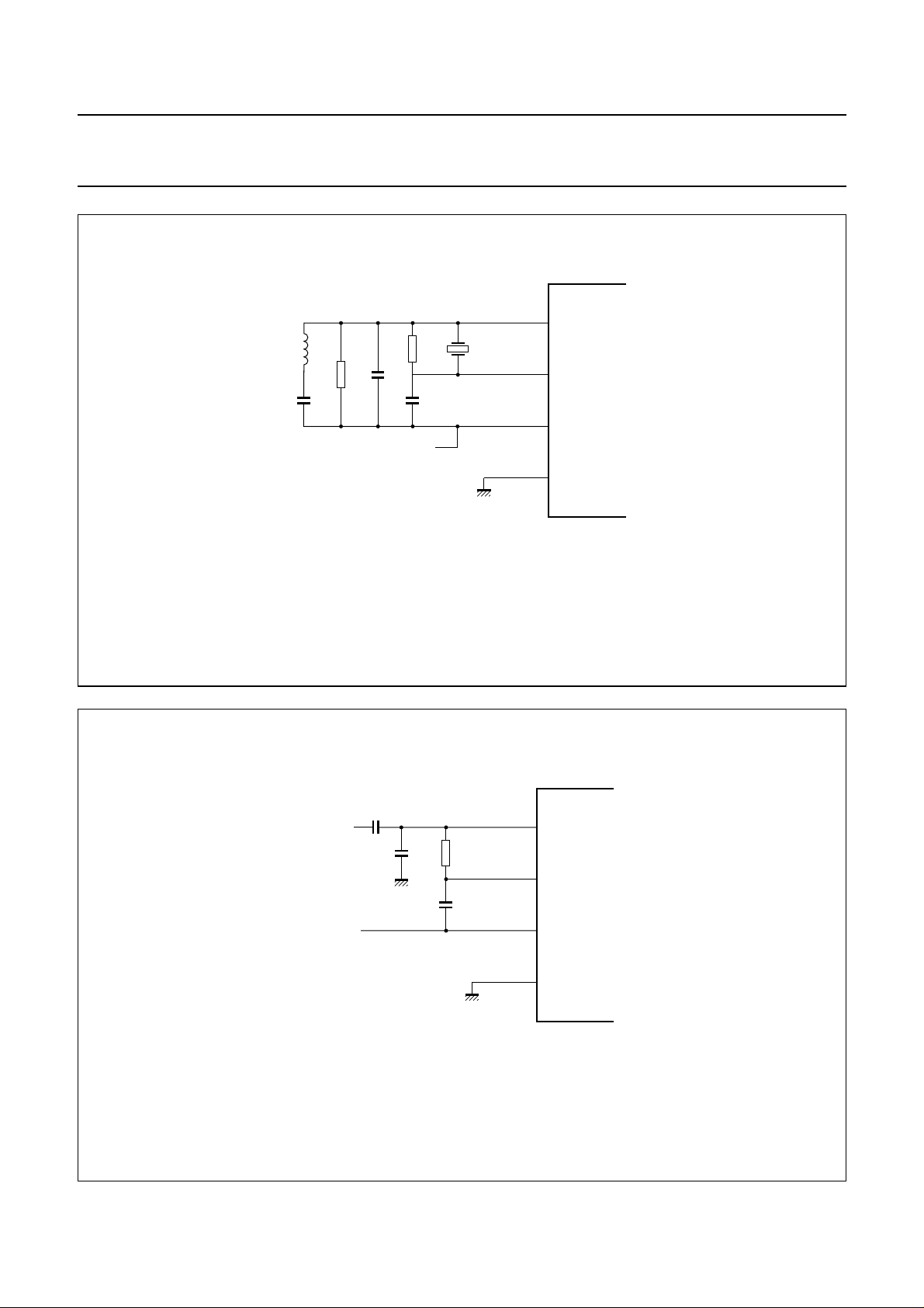
Clock generation and distribution
The clock generation section of the TDA1307 is designed
to accommodate two main modes. The master mode, in
which the TDA1307 is the master in the digital audio
system, and for which the clock is generated by connecting
a crystal of 768f
(33.8688 MHz) to the crystal oscillator
s
pins XTAL1 (pin 22) and XTAL2 (pin 23); and the slave
mode, in which the TDA1307 is supplied a clock by the IC
in the system that acts as the master (e.g. the digital audio
interface receiver). In this event a clock signal frequency of
256fs is input to pin XTAL1. Master or slave mode is
programmed by means of pin CDCC (pin 18) logic 1 for
master and logic 0 for slave mode. The circuit diagram of
Fig.4 shows the typical connection of the external
oscillator circuitry and crystal resonator for master mode
operation. Note that the positive supply V
DDOSC
is the
reference to the oscillator circuitry. The LC network is used
for suppression of the fundamental frequency component
of the overtone crystal. Figure 5 shows how to connect for
slave mode operation. A clock frequency of typical 256f
and levels of 0 V/+5 V is input to XTAL1 via AC coupling.
The 100 kΩ resistor and the 10 nF capacitor are required
to provide the necessary biasing for XTAL2 by filtering and
feeding back the output signal of XTAL1.
Besides generating all necessary internal clocks for the
audio data processing blocks and the clock to the DAC, the
clock generation block further provides two clocks for
external use when operating in master mode. Pin CDEC
(pin 7) is used as the running clock for the system
decoder IC, and pin CMIC (pin 15) is used as the running
clock for the system microprocessor. CMIC outputs, by a
fixed divider ratio to XTAL2, a clock signal at 96fs. For
CDEC the divider ratio is programmable by means of pins
CLC1 (pin 14) and CLC2 (pin 17). Table 1 gives the clock
divider programming relationships.
s
Table 1 Clock divider programming
CLC1 CLC2 CDEC OUTPUT FREQUENCY
0 0 256f
0 1 384f
1 0 768f
1 1 192f
1996 Jan 08 7
s
s
s
s
Page 8
Philips Semiconductors Preliminary specification
High-performance bitstream digital filter TDA1307
handbook, halfpage
XTAL2
23
3.3
µH
1 nF
10
kΩ
10
pF
100
+5 V
kΩ
10
pF
33.8688
MHz
V
V
XTAL1
DDOSC
SSOSC
22
TDA1307
24
25
MGB981
Fig.4 External crystal oscillator circuit.
handbook, halfpage
fi = 256f
s
+5 V
20 pF
30
pF
100 kΩ
10 nF
XTAL2
XTAL1
V
DDOSC
V
SSOSC
23
22
TDA1307
24
25
MGB982
Fig.5 External clock input connections.
1996 Jan 08 8
Page 9
Philips Semiconductors Preliminary specification
High-performance bitstream digital filter TDA1307
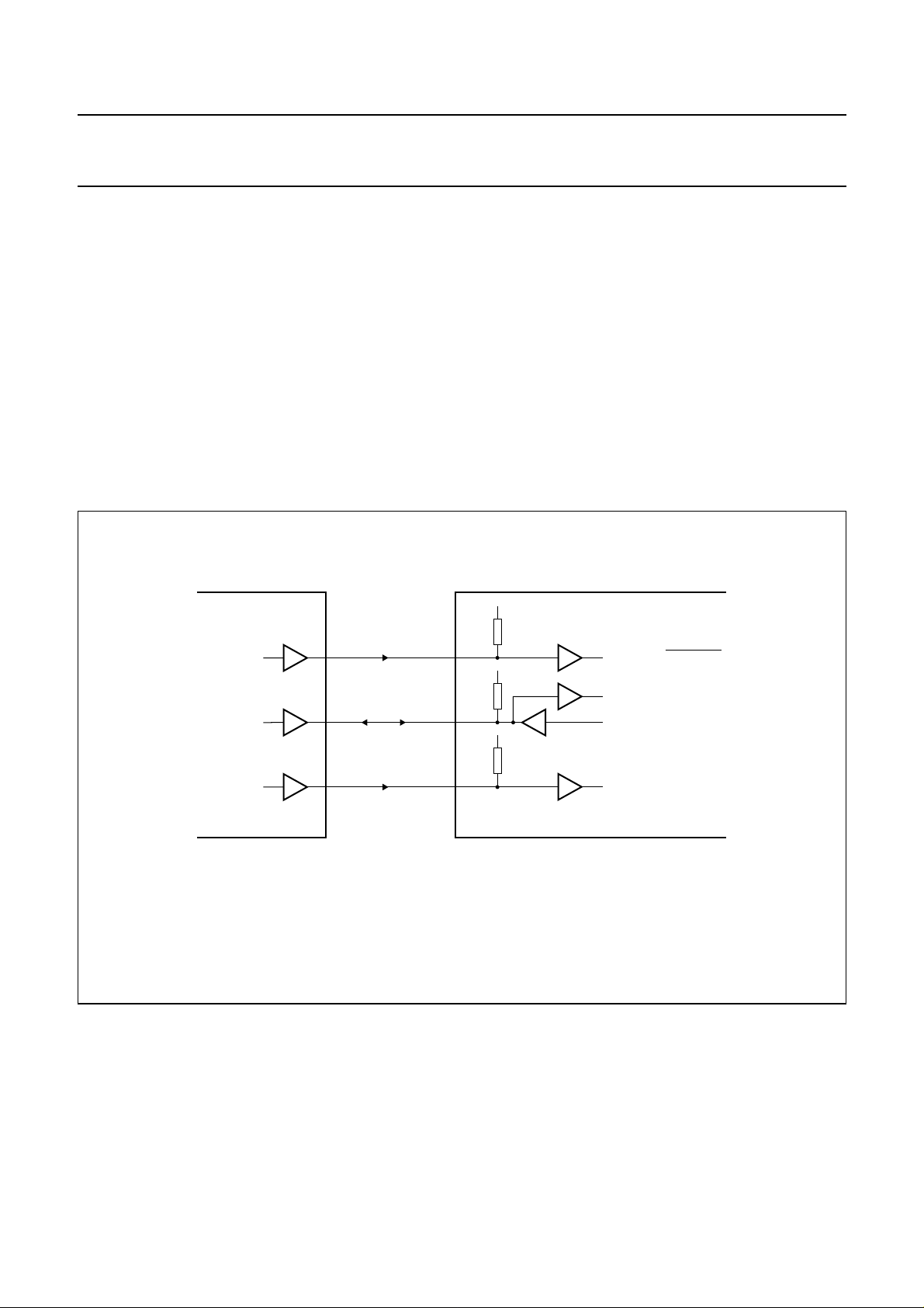
Microprocessor interface
The microprocessor interface provides access to virtually
all of the functional blocks in the audio data processing
section. Its destination is two-fold: system constants (such
as input format and sample frequency) as well as system
variables (attenuation, muting, de-emphasis, volume
control data etc.) can be ‘written to’ the respective blocks
(command mode), and continuously collected stereo peak
data ‘read from’ the peak detection block (peak request).
The system settings are stored in the TDA1307 in an
internal register file. Peak data is read from the stereo
peak value register.
handbook, full pagewidth
RAB 42
DA/ACK 38
THREE-LINE MICROPROCESSOR INTERFACE BUS
Communication is realized by a three-line bus, consisting
of the following signals (see Fig.6):
• Clock input CL (pin 39), to be generated by the
microprocessor
• Command/request input RAB (pin 42), by which either
of the two mode commands (RAB = 0) and peak request
(RAB = 1) are invoked
• Bidirectional data line DA (pin 38), which either receives
command data from the microprocessor or outputs peak
data from the peak detection block.
CL and RAB both default HIGH by internal pull-up, DATA
is 3-state (high impedance, pull-up, pull-down).
+
REQUEST/COMMAND
+
COMMAND DATA
PEAK DATA
+
CL 39
MICROPROCESSOR
Fig.6 Three-line microprocessor interface bus.
1996 Jan 08 9
CLOCK
TDA1307
MGB984
Page 10

Philips Semiconductors Preliminary specification
High-performance bitstream digital filter TDA1307
INITIALIZATION OF THE BUS RECEIVER
The microprocessor interface section is initialized
automatically by the power-on reset function, POR
(pin 20). A LOW input on POR will initiate the reset
procedure, which encompasses a functional reset plus
setting of the initial states of the control words in the
command register file. A wait time of at least one audio
sample time after a LOW-to-HIGH transition of POR must
be observed before communication can successfully be
established between the TDA1307 and the
microprocessor. In addition to the POR function, a
software reset function issued from the microprocessor is
provided (see section “Organization and programming of
the internal register file”), which has the sole function of
reinstating the initial values of the microprocessor control
register. More information on initializing the TDA1307 can
be found under “Application Information”.
C
OMMAND PROTOCOL
The protocol for writing data to the TDA1307 is illustrated
in Fig.7. The command mode is invoked by forcing RAB
LOW. A unit command is given in the form of an 8-bit burst
on the DA line, clocked on the rising edge of CL.
The command consists of 4 address bits followed by
4 control data bits (both MSB first). A next command may
be immediately issued while keeping RAB forced LOW.
Only commands for which the MSB of the address bits is
LOW are accepted; of the remaining set of addresses, only
four have meaning (see section “Organization and
programming of the internal register file”). The command
input receiver is provided with a built-in protection against
erroneous command transfer due to spikes, by a 2-bit
debounce mechanism on lines DA and CL. The
waveforms on these lines are sampled by the receiver at
the internal system clock rate 256f
. A state transition on
s
DA or CL is accepted only when the new state perseveres
for two consecutive sampled waveform instants.
O
RGANIZATION AND PROGRAMMING OF THE INTERNAL
REGISTER FILE
Command data received from the microprocessor is
stored in an internal register file (see Table 2), which is
organized as a page of 10 registers, each containing a
4-bit command data word (D3 to D0). Access to the words
in the register file involves two controls: selection of the
address of a set of registers (by means of A3, A2,
A1 and A0) and setting the number of the bank in which
the desired register is located (by means of the ‘bank bits’
B0 and B1). First the desired bank is selected by
programming the command word at address 0000
(supplying the bank bits plus refreshing bits ATT and DIM).
A subsequent addressing (one of three addresses, 1H, 4H
and 6H) will yield access to the register corresponding to
the last set bank.
handbook, full pagewidth
RAB
CL
DA (TDA1307)
DA (µP)
DA
t
DRW
t
CKL
1
t
DSM
A3 A2 A1 A0 D3 D2 D1 D0
A3 A2 A1 A0 D3 D2 D1 D0
t
t
CKH
Fig.7 Microprocessor command protocol.
1996 Jan 08 10
t
DHM
8
MGB995
Page 11

Philips Semiconductors Preliminary specification
High-performance bitstream digital filter TDA1307
Table 2 Microprocessor control register file
ADDRESS
A3 A2 A1 A0
BANK
B0 B1
0000X XBANK B0 BANK B1 ATT DIM 0 0 1 1
00010 1FCON DIT FSS9 FSS8 0 0 0 0
1 0 FSS7 FSS6 FSS5 FSS4 0 0 1 0
1 1 FSS3 FSS2 FSS1 FSS0 1 0 0 0
01000 1DCEN DCSH FN9 FN8 0 1 1 1
1 0 FN7 FN6 FN5 FN4 0 0 0 0
1 1 FN3 FN2 FN1 FN0 1 1 0 1
01100 1DEMC1 DEMC0 RES0 RES1 0 0 0 0
1 0 INS1 INS0 FS1 FS0 0 0 0 0
1 1 RES2 NS RST STBY 1 0 0 0
Following is a list of the programming values for the
various control words in the register file. Information on the
meaning of the different controls can be found under the
sections covering the corresponding signal processing
blocks (see sections “Multiple format input interface” to
“Third and fourth order noise shaping”).
BANK B0, BANK B1
D3 D2 D1 D0 INITIAL STATE
DIT
Dither control bit: logic 1 to activate dither addition, logic 0
deactivates.
FSS9 to FSS0
Fade function 10-bit control value to program fade speed,
in number of samples per fade step.
Programming of the bank bits is given in Table 2. The bank
bits can be changed by addressing register location 0000.
Subsequent addressing will result in access of locations
according to the last selected bank.
ATT
Attenuation control bit: logic 1 to activate −12 dB
attenuation, logic 0 to deactivate. As the attenuate control
bit shares a control word with the bank bits, ATT has to be
refreshed each time a new bank is selected.
DIM
Digital mute control bit: logic 1 to activate mute, logic 0 to
deactivate. An active digital mute will override the
attenuation function. As with ATT, DIM needs to be
refreshed with each change in bank selection.
FCON
Fade function control bit: logic 1 to activate the fade
function, logic 0 to deactivate.
DCEN
DC-filter enable bit: logic 1 enables subtraction of the
DC-level from the input signal, logic 0 disables.
DCSH
DC-filter sample or hold control bit: when DCSH = 0 the
DC-level of the input signal is continuously evaluated.
When DCSH = 1 the once acquired DC value, to be
subtracted from the input signal, is held constant.
FN9 to FN0
Fade function 10-bit control value to program volume level.
DEMC1, DEMC0
De-emphasis function enable and fs selection bits.
1996 Jan 08 11
Page 12

Philips Semiconductors Preliminary specification
High-performance bitstream digital filter TDA1307
Table 3 De-emphasis mode programming
DEMC1 DEMC0 DE-EMPHASIS FUNCTION
0 0 de-emphasis disabled
0 1 de-emphasis for f
1 0 de-emphasis for f
1 1 de-emphasis for f
= 32.0 kHz
s
= 44.1 kHz
s
= 48.0 kHz
s
Table 4 Input format programming
INS1 INS0 INPUT FORMAT
2
00I
S up to 20 bits
0 1 Sony format 16 bits
1 0 Sony format 18 bits
1 1 Sony format 20 bits
Table 5 Sample frequency indication programming
FS1 FS0
00f
01f
DOBM SAMPLE
FREQUENCY INDICATION
= 44.1 kHz
s
= 48.0 kHz
s
1 0 no meaning
11f
= 32.0 kHz
s
RES2 to RES0
These are reserved locations and have no functional
meaning in the TDA1307.
INS1, INS0
Input format selection control bits.
FS1, FS0
RST
Software reset function. When RST = 1 the contents of the
microprocessor control registers will immediately be
preset to their initial values as shown in Table 2. As part of
this reset action, bit RST is automatically returned to its
initial state 0, that being normal operation.
STBY
Standby mode control bit. When STBY = 1 the standby
mode will be initiated (explained under the section treating
the Digital Output block). STBY = 0 for normal activity.
EAK DATA OUTPUT PROTOCOL
P
The peak data read-out protocol is illustrated in Fig.8.
A peak request is performed by releasing RAB (which will
be pulled HIGH by TDA1307) while CL = HIGH, and
maintaining RAB = 1 throughout the peak data
transmission. TDA1307 will acknowledge the peak request
by returning a LOW state on the DA line. Upon this peak
acknowledge, the microprocessor may commence
collecting data from the internal peak data output register
(16-bit Left, 16-bit Right channel peak data) by sending a
clock onto the CL line. The contents of the peak data
output register will not change during the peak request.
The first peak bit, the MSB of the Left channel peak value,
is output upon the first LOW-to-HIGH transition of CL.
To access Right channel peak value, all 16 bits of channel
Left have to be read out, after which up to 16 bits of Right
channel peak data may be read out. The peak data read
out procedure may be aborted at any instant by returning
RAB LOW, marking the end of the peak request: the
internal peak register will be reset and the peak detector
will start collecting new peak data and transferring this to
the peak data output register.
Sample frequency indication control bits for the digital
output section.
NS
Control bit for Noise Shaper section. When NS = 0, 3rd
order noise shaping is selected; when NS = 1, 4th order
noise shaping is selected.
1996 Jan 08 12
Page 13

Philips Semiconductors Preliminary specification
High-performance bitstream digital filter TDA1307
handbook, full pagewidth
RAB
CL
DA (TDA1307)
DA (µP)
DA
t
DWR
t
DSP
Fig.8 Peak data output protocol.
Multiple format input interface
Data input to the TDA1307 is accepted in four possible
formats, I2S (with word lengths of up to 20 bits), and Sony
formats of word lengths 16, 18 and 20-bit. The general
appearance of the allowed formats is given in Fig.9. The
selection of a format is achieved through programming of
the appropriate bits in the microprocessor register file.
Characteristic timing for the input interface is given in the
diagram of Fig.10.
S
YNCHRONIZATION
For correct data input to reach the central controller of
TDA1307, synchronization needs to be achieved to the
incoming 1fs I2S or Sony format input signals.
The incoming WS signal is sampled to detect whether its
phase transitions occur at the correct synchronous timing
instants. This sampling occurs at the TDA1307 internal
clock rate, 256fs. After one phase transition of WS, the
next is expected after a fixed delay, otherwise the
condition is regarded as out-of-lock and a reset is
performed, this operation is repeated until synchronization
is achieved. To allow for slight disturbances causing
unnecessary frequent resets, the critical WS transitions
are expected within a tolerance window (−4 to +4 periods
of the 256fs internal sampling clock instants).
READ PEAK DATA
t
DHP
Q11Q2 Q3 Q31 Q32
Q1 Q2 Q3 Q31 Q32
MGB996
The reset action is flagged on the RESYNC (pin 19)
output, which may be optionally used for muting or related
purposes. RESYNC becomes HIGH the instant a reset is
initiated, and remains in that state for at least one sample
period (1/f
E
RROR FLAG INPUT EFAB
).
s
The error flag input EFAB (pin 4) is intended as request
line from the system decoder to the digital filter to indicate
erroneous audio samples requiring concealment.
A detected HIGH on input EFAB will be relayed by the
input interface block to the error concealment block, where
the samples flagged as erroneous will be processed
accordingly.
1996 Jan 08 13
Page 14

1996 Jan 08 14
a
ndbook, full pagewidth
Philips Semiconductors Preliminary specification
High-performance bitstream digital filter TDA1307
SCK
EFAB
WS
SD
SCK
WS
SD
12
LEFT
MSB
B2
SAMPLE IN LEFT
INPUT FORMAT I
12345678910 2324 23 2412345678910
LEFT RIGHT
32 1 2n3212n
RIGHT
MSB
SAMPLE IN RIGHT
2
S
MSB
B2 B15 LSB
SAMPLE IN LEFT
B2 MSB
INPUT FORMAT SONY 16-BIT
B2
SAMPLE IN LEFT
MSB B15B2 LSB
SAMPLE IN RIGHT
SD
SD
MSB B2 B3 B4 B17 LSB
SAMPLE IN LEFT
MSB B2 B3 B4 B5 B6 B19 LSB
SAMPLE IN LEFT
INPUT FORMAT SONY 20-BIT
Fig.9 Input formats.
INPUT FORMAT SONY 18-BIT
MSB B2 B3 B4 B5 B6 B19 LSB
MSB B2 B3 B4 B17 LSB
SAMPLE IN RIGHT
SAMPLE IN RIGHT
MGB999
Page 15

Philips Semiconductors Preliminary specification
High-performance bitstream digital filter TDA1307
handbook, full pagewidth
WS
SCK
SD
RIGHT
LEFT
trtHBtft
LB
t
HD;WS
Fig.10 Typical I2S-bus data waveforms.
Error concealment, interpolation and muting
The error concealment functional block performs three
functions:
1. interpolation of up to eight consecutive erroneous
audio samples flagged as such by input EFAB
2. attenuation
3. muting of incoming audio, both the latter if so activated
by means of the microprocessor registers.
Furthermore, as these functions constitute error
processing functions, operation of any of these functions is
reported to the digital output DOBM by setting the validity
flag.
RIGHT
LEFT
t
SU;WS
t
SU;DAT
t
HD;DAT
MGB998
initiated over the maximum interpolation interval of eight
sampling instants.
A
TTENUATION
The concealment block incorporates a digital −12 dB
attenuation function intended to be used in program
search or other player actions that may generate audible
transitional effects such as loud clicks. The attenuate
function is activated by means of bit ATT in the
microprocessor register file. Setting this bit to logic 1
causes the next audio sample (attenuate never takes
action on incomplete samples) to be attenuated with
immediate effect (the validity flag of the digital audio output
DOBM is set).
E
IGHT-SAMPLE INTERPOLATION
Incoming audio samples may be visualized as entering a
memory pipeline, nine audio sample instants in depth,
upon entering the error concealment block. Any audio
samples marked as erroneous by the flag input EFAB will
be reconstructed by linear approximation from the values
of the adjacent correct samples (the last correct sample
still available, and the next correct sample). The linear
interpolation is started as soon as a correct sample
becomes available within nine sampling instants. Should a
flagged erroneous condition persevere for over eight
sampling instants, then the last correct sample will be held
for as long as necessary, i.e. until the next correct sample
enters the pipeline. The linear approximation is then
1996 Jan 08 15
The interpolation facility is called upon when an attenuate
command is given while the incoming data is flagged as
invalid by EFAB. If no more than eight samples in
succession are invalid, attenuate may take immediate
effect (this causes the output value to ramp linearly to the
final attenuated level). If nine or more samples in a row are
flagged erroneous, attenuation is postponed and the last
good sample held, until the next good sample becomes
available. Upon that instant, the output ramps linearly,
over the maximum interpolation time span, to the
attenuated first correct sample. Releasing attenuate (bit
ATT reset to 0) always has immediate effect (i.e. the next
complete audio sample will pass unattenuated).
Page 16

Philips Semiconductors Preliminary specification
High-performance bitstream digital filter TDA1307
MUTING
The digital mute of the error concealment block
immediately (i.e. on the next whole audio sample) sets the
input to the digital filter to all zeros, regardless of any other
current action in the error concealment block. The digital
mute function is activated by means of bit DIM in the
microprocessor register file. Setting this bit to logic 1
causes the next audio sample to be muted (the validity flag
of the digital audio output DOBM is set).
Releasing the digital mute function (resetting bit DIM to 0)
will cause the output of the error concealment block to
approach the unaffected audio sample value by linear
approximation, on the condition that the mute action
spanned at least 8 consecutive audio samples. If there are
samples in error at the time of releasing mute, the release
action is postponed until good data becomes available,
after which the linear ramp can be made over the
maximum interpolation time span.
Digital output (DOBM)
The DOBM block constructs a biphase modulated digital
audio output signal which complies to the IEC standard
958, to be used as a digital transmission link between
digital audio systems. A variety of inputs are combined,
arranged and modulated to finally form the output
biphase-mark sequence. The inputs are the following:
• left and right audio data, word length 20-bit, as delivered
by the error concealment block
• the Validity flag as output by the error concealment block
• subcode information, as acquired by input via pins
SBDA (pin 6) and SBCL (pin 5)
• sampling frequency information as set by means of
bits FS1 and FS0 in the microprocessor register file.
As the digital output function is not always required, and
can give rise to interference problems in high-quality audio
conversion systems, the DOBM output can be switchedon
or off by means of pin DSTB (digital output standby, 13).
Leaving DSTB open-circuit will cause it to pull HIGH and
deactivate the DOBM output; tying DSTB LOW enables
the digital output function.
The programming of bits FS1 and FS0 is specified in
Table 5 under section “Microprocessor interface”. The
DOBM block of TDA1307 translates the settings of these
bits to the appropriate corresponding information in the
digital audio output sequence (as specified by IEC 958).
The inputs SBDA (subcode data, 6) and SBCL (subcode
clock, 5) allow for the merging of subcode data into the
output DOBM signal. The input sequence via these inputs
is defined as 10-bit burst words, arranged as illustrated in
Fig.11; the bit nomenclature corresponds to that used in
the IEC standard 958. Both subcode data and clock
signals are normally supplied by the decoder of the digital
audio system (e.g. SAA7310).
For set-up and hold timing of the SBDA and SBCL inputs,
restrictions identical to the audio data inputs are valid.
handbook, full pagewidth
SBCL
Q-CHANNEL PARITY
CHECK FLAG
(0 = FAIL)
SUBCODING
ERROR FLAG
W V U T S R Q P-BITP-BITSBDA
Fig.11 Format of subcode data input.
1996 Jan 08 16
SYNC (active LOW)
MGB997
2.8224 MHz (typ.) BURST CLOCK
Page 17

Philips Semiconductors Preliminary specification
High-performance bitstream digital filter TDA1307
Digital silence detection
The TDA1307 is designed to detect digital silence
conditions in channels left and right, separately, and report
this via two separate output pins, one for each channel,
DSL (pin 11) and DSR (pin 12). This function is
implemented to allow for external manipulation of the
audio signal upon absence of program material, such as
muting or recorder control. The TDA1307 itself does not
influence the audio signal as a result of digital silence; the
sole function of this block is detection, and any further
treatment must be accomplished externally.
An active LOW output is produced at these pins if the
corresponding channel carries either all zeroes for at least
8820 consecutive audio samples
(200 ms for f
The digital silence detection block receives its left and right
audio data from the error concealment block (implying that
a digital mute action will produce detection of a digital
silence condition), and passes it unaffected to the next
signal processing stage, the de-emphasis block.
De-emphasis filter
The TDA1307 incorporates selectable digital de-emphasis
filters, dimensioned to produce, with extreme accuracy,
the de-emphasis frequency characteristics for each of the
three possible sample rates 32, 44.1 and 48 kHz. As a
20-bit dynamic range is maintained throughout the filter,
considerable margin is kept with respect to the normal CD
resolution of 16-bit i.e. the digital de-emphasis of TDA1307
is a truly valid alternative to analog de-emphasis in
high-performance digital audio systems.
= 44.1 kHz).
s
degradations in processing the mentioned types of
excitations. To dimension a high-fidelity digital filter, a
balance must be established between filter steepness and
overload susceptibility.
The oversampling digital filter function in the TDA1307 is
designed, in combination with the noise shaper, to deliver
the highest fidelity in signal reproduction possible. Not only
are stop-band suppression and pass-band ripple
parameters to the design, but also the prevention of
detrimental artifacts of too extreme filtering: impulse and
high-level overload responses. The outcome is a patented
design excelling in natural response to most conceivable
audio stimuli. It is realized as a series of three half-band
filters, each oversampling by a ratio of two, thus achieving
an eight times oversampled and interpolated data output
to be input to the noise shaper. Each stage has a finite
impulse response with symmetrical coefficients, which
makes for a linear phase response. Filter stages 1, 2 and
3 incorporate 119, 19 and 11 delay taps respectively.
To maintain an output accuracy of 20 bits, an internal data
path word length of 39 bits is used to supply the required
headroom in multiplications. Requantization back to 20-bit
word length is performed by noise shaping (thus effectively
preventing rounding errors in so far as they have effect in
the audio frequency band), at the output of each filter
section.
The successive half-band filter stages are, for efficiency,
distributed over the audio data processing path:
DC-filtering, peak value reading and volume control are
performed between stages 1 and 2 (the 2f
DC-cancelling filter
domain).
s
Selection of the de-emphasis filters is performed via the
microprocessor interface, bits DEMC1 and DEMC0, for
which the programming is given in Table 3.
Oversampling digital filter
The oversampling digital filter in the digital audio
reconstruction system is of paramount influence to the
fidelity of signal reproduction. Not only must the filter
deliver a desired stop-band suppression while sustaining a
certain tolerated pass-band ripple, but it must also be
capable of faithfully reproducing signals of high energy
content, such as signals of high level and frequency,
square wave-type signals and impulse-like signals (all of
these examples have their counterparts in actual music
program material). Filters optimized only towards
pass-band ripple and stop-band suppression are capable
of entering states of overload because of the clustered
energy content of these signals, thus introducing audible
1996 Jan 08 17
A mechanism for optionally eliminating potential DC
content of incoming audio data is implemented in the
TDA1307 for three main reasons. Most importantly
because it is called for by the implementation of volume
control in the TDA1307. An audio signal that is to be
subjected to volume control (multiplication by a controlled
attenuation factor) should be free of offset, otherwise the
controlled multiplication will produce the undesired side
effect of modulating the average DC content. The second
reason is supplied by the implementation of audio peak
data read-out in the TDA1307. As the peak value is
obtained from the absolute value of the audio data
referenced to zero DC level, its accuracy is impaired by the
presence of residual DC information, progressively so for
lower audio levels. The third reason is brought about by
application of the noise shaper. To optimize the dynamic
behaviour of the noise shaper especially for low-level
signals, it is supplied a predefined offset, sometimes
referred to as DC dither. Taking no precautions against DC
Page 18

Philips Semiconductors Preliminary specification
High-performance bitstream digital filter TDA1307
content of the source audio data may render the DC dither
potentially ineffective.
In applications where the DC content of the audio
information may be expected, application of the selectable
DC filter may be opted for. It is implemented as a first-order
high-pass filter with a corner frequency of 2 Hz. Control of
the DC filter is achieved by accessing the appropriate bits
DCEN (DC filter enable) and DCSH (DC filter sample or
hold) in the microprocessor register file. The principle of
operation is illustrated in Fig.12. The output of the DC filter,
referred to in the diagram as ‘audio output’ always equals
the audio input subtracted by the output of the low-pass
branch. Depending on the control bit DCSH, this
subtraction value is either the last value held constant or
a value continuously adapting to incoming DC content.
The DC filter is effectively switched on or off via control bit
DCEN, which selects the input of the low-pass section
either to be the audio input data (the output of the low-pass
section will settle to the low frequency content of the audio
data so that the filter is on) or a preset value of zero
(low-pass output will settle to zero meaning ‘filter off’).
The constant mode is implemented to provide a mode in
which a stable subtraction value is guaranteed; in this
mode however the high-pass function is inhibited so there
is no adaptation to changes in the DC content of the
incoming source information.
Peak detection
The TDA1307 provides a convenient way to monitor the
peak value of the audio data, for left and right channels
individually, by way of read-out via the microprocessor
interface. Peak value monitoring has its applications
mainly in digital volume unit measurement and display,
and in automatic recording level control. The peak level
measurement of the TDA1307 occurs with a resolution of
16-bit, providing a dynamic range amply suitable for all
practical applications.
The output of the peak detection block is a register of two
16-bit words, one for each channel, representing the
absolute value of the accumulated peak value, accessible
via the microprocessor interface. The peak detection block
continuously monitors the audio information arriving from
the DC-cancelling filter, comparing its absolute value to
the value currently stored in the peak register. Any new
value greater than the currently held peak value will cause
the register to assume the new, greater value. Upon a
peak request (for which the protocol is described in section
“Peak data output protocol”), the contents of the peak
register are transferred to the microprocessor interface.
After a read action, the peak register will be reset, and the
collection of new peak data started.
The peak detection block receives data that has been
processed by the first half-band stage of the oversampling
interpolating digital filter (in the 2fs domain, but the peak
detection ‘samples’ at 1fs for efficiency). This means that
the scaling applied in this first half-band stage is noticeable
in the measured peak value. The frequency-independent
attenuation factor of the first half-band filter equals
0.175 dB - this results in a possible range for the output
peak value of 0 to 32114. When the audio signal may be
expected to carry DC content, use of the DC cancelling
filter of TDA1307 is recommended, to ensure correct and
accurate peak detection.
handbook, full pagewidth
audio input
from first
half-band stage
zero
DCEN = 1
DCEN = 0
LPF
fo = 2 Hz
Fig.12 Schematic diagram of the DC filter.
1996 Jan 08 18
DCSH = 0
DCSH = 1
+
−
T
audio output
+
to peak
detection block
MGB994
Page 19

Philips Semiconductors Preliminary specification
High-performance bitstream digital filter TDA1307
handbook, full pagewidth
from
microprocessor
register file
audio input
from peak
detection block
FN
(desired level)
FSS
(fade speed)
FCON
10
10
Fig.13 Schematic diagram of the volume control block.
Fade function and volume control
One of the main features of TDA1307 is a patented,
advanced digital volume control with inherent fading
function, exhibiting an accuracy and smoothness
unsurpassed in presently available digital filters. Only the
desired volume and the fade speed need to be instructed
to the TDA1307, which can be realized in a single
instruction via the microprocessor interface. The volume
control function then autonomously performs automatic
fade in or fade out to the desired volume by a natural,
exponential approach. It allows for volume control to an
accuracy of 0.1 dB over the range from 0 dB of full scale to
beyond −100 dB. The speed of approach can be set over
a wide range, varying from less than one second to over
23 seconds for a complete fade. Furthermore the fade
algorithm manages the additional fading resolution, in
excess of the 0.1 dB available for the volume desired level,
needed to ensure gradual changes in volume at all times.
Figure 13 illustrates the volume control block.
Three data entities in the microprocessor register file
pertain to the volume control block: a 10-bit control value
for the desired volume (bits FN9 to FN0), a 10-bit control
value for the fade speed (bits FSS9 to FSS0), and the fade
function override bit, FCON. The volume control word
ranges from 0 (representing a desired volume level or
0 dB) to 1023 (representing maximum desired volume
level of zero or −∞ dB). For values 1 to 1023, an LSB
change of the volume control word represents 0.1 dB
change of volume level. In changing from one volume level
to the next desired volume level, the volume control block
audio output
to second
half-band stage
controlled
multiplication
18
factor
VOLUME
CONTROL
ALGORITHM
MGB985
calculates and applies intermediate volume levels
according to an exponential approach curve. The speed at
which the approach curve progresses is determined by the
value of the fade speed control word, FSS. FSS + 2 is the
amount of time delay applied, in units of audio sample
instants, before a next value on the exponential curve is
calculated and applied.
The total duration of an exponential fade operation is the
product of the desired amount of volume change FN (in
LSBs of the 10-bit control word) and the amount of delay
per fade step FSS (in LSB times seconds), expressed as
follows:
t
fade, exp, total
where f
is the base-band sampling frequency.
s
∆FN
----------------------------f
s
,
FSS 2+()
×=
Thus the longest fade time achievable, occurring in the
event of maximum desired volume change ∆FN = 1023,
slowest speed setting FSS = 1023, and in the event that
f
= 44.1 kHz, is 23.7 seconds.
s
To smooth out fast volume changes however, the
TDA1307 fade function adds extra resolution to the
volume control by gradually changing from one
exponential step to the next, by a linear transition.
Whereas the 10-bit FN-value could not accomplish
discrete attenuation steps finer than 0.1 dB, the linear
transitional approach enhances volume change resolution
to 15-bit. The volume level therefore never changes faster
than one LSB of the 15-bit attenuation factor per audio
sample. As soon as the linear transition reaches the value
1996 Jan 08 19
Page 20

Philips Semiconductors Preliminary specification
High-performance bitstream digital filter TDA1307
determined by the exponential approach, the attenuation
value remains stable until the next exponential value is
due, which will again initially be approached linearly. For
exponential fade speeds higher than the linear approach
can follow, the approach remains linear unless the
exponential approach curve is intersected. For fast volume
decrease, the start of the approach will be linear, whereas
for a fast volume increase, the course of the fade approach
will be exponential at first, then saturating to linear.
The fastest fade speed, for large volume changes, is
therefore determined by the linear approach. For a
maximum volume change at maximum speed, follows a
fade time of (215− 1)/44100 = 0.74 seconds.
For immediate return to the maximum volume level without
altering the volume and fade speed settings, bit FCON in
the register file can be used. With this bit set to 1, the fade
function is active and operates as described above.
Resetting FCON to 0 will immediately deactivate the fade
function, that is, return the volume level to maximum at the
start of the next audio sample. Changing state of FCON
from 0 to 1 will cause a fade according to the current
settings of volume and speed control words FN and FSS.
In Fig.14, a few fading examples illustrate the operation of
the TDA1307 advanced digital volume control.
Dither and scaling
Prior to input to the noise shaper, final preprocessing is
performed upon the eight times oversampled and
interpolated audio data stream in the form of scaling and
dither addition. The fixed scaling factor, a
frequency-independent attenuation of 3 dB, is applied to
the signal in order to provide the noise shaper with
sufficient headroom. The application of dither is optional,
selectable by means of bit DIT in the microprocessor
register file.
With DIT set to 1, fixed dither levels of value 2
2−6− 2−5 are added alternately to the audio signal, at an
alternation rate of 4fs. This amounts to a combination of an
AC dither signal of frequency 4fs and amplitude −24 dB of
full-scale, with a DC dither (offset) of 3.125% of full-scale
peak amplitude. With DIT set to 0, no dithering, AC or DC,
is performed.
−6+2−5
and
Third and fourth order noise shaping
The noise shaper constitutes the final audio processing
stage of TDA1307, which takes the eight times
oversampled and interpolated audio data stream from the
digital filter as input, and by extreme oversampling and
1-bit end quantization processes the signal so that it can
be converted to analog by a one-bit digital-to-analog
converter. The order of the noise shaper is selectable,
between 3rd and 4th order, by means of the register file bit
NS (NS = 0: 3rd order, NS = 1: 4th order). Together with
the final oversampling ratio, the noise shaper order
determines the dynamic range (or accuracy) that the noise
shaper can achieve (the oversampling ratio will depend on
the system clock frequency and application mode used).
Table 6 gives the dynamic range of the noise shaper as a
function of these two parameters.
Figures 15 and 16 show noise spectral density simulations
of the third and fourth order noise shaper respectively, with
a stimulus frequency of 1 kHz at a level of −10 dBfs, for
192 × 44.1 kHz oversampling. From the slope of the
shaped noise spectrum outside the audio band, the order
of noise shaping is apparent. It is important to note that, in
contrast to normal fourth-order noise shaping, where an
audio post-filter of equal order would be needed to
compensate the slope of the quantization noise, the
fourth-order noise shaper of the TDA1307 actually only
needs third order post-filtering to obtain the same amount
of stop-band suppression as with third order. The noise
density of the fourth order noise shaper starts at a lower
level for low frequencies, and only slightly exceeds the
third-order curve in the 200 to 300 kHz region.
Although the addition of dither is made selectable in the
TDA1307, it is generally recommended for use always, as
dither is essential to the accurate conversion of low-level
signals and reproduction of silence conditions by
noise-shaping circuits.
1996 Jan 08 20
Page 21

Philips Semiconductors Preliminary specification
High-performance bitstream digital filter TDA1307
handbook, full pagewidth
max
volume
level
0.1 dB
(FSS + 2)/f
1/f
s
s
0
A
A: Fade out to zero (FN = 0).
B: Fade in to maximum volume (FN = 1023).
C: Fast volume decrease resulting in initial linear regulation.
D: Slow volume decrease predominantly exponential.
E: Volume regulation overridden by resetting FCON to 0.
F: FN = 0, FSS = 0, FCON to 1 causes fastest maximum fade with linear regulation.
G: Medium speed volume increase starts exponential, ends linear.
B
CD E F G
Fig.14 Volume control examples.
Table 6 Noise shaper dynamic range
OVERSAMPLING/ORDER 3rd ORDER 4th ORDER
128f
s
192f
s
time
MGB991
105 dB 118 dB
117 dB 134 dB
1996 Jan 08 21
Page 22

Philips Semiconductors Preliminary specification
High-performance bitstream digital filter TDA1307
handbook, full pagewidth
0
A
o
(dBfs)
−50
−100
−150
−200
10 10
2
3
10
4
10
Fig.15 Noise shaper output spectrum (N = 3; 192fs).
5
10
log frequency (Hz)
MGB992
6
10
handbook, full pagewidth
0
A
o
(dBfs)
−50
−100
−150
−200
10 10
2
3
10
4
10
Fig.16 Noise shaper output spectrum (N = 4; 192fs).
5
10
log frequency (Hz)
MGB993
6
10
1996 Jan 08 22
Page 23

Philips Semiconductors Preliminary specification
High-performance bitstream digital filter TDA1307
LIMITING VALUES
In accordance with the Absolute Maximum Rating System (IEC 134).
SYMBOL PARAMETER CONDITIONS MIN. MAX. UNIT
V
DD
V
I
I
IK
I
OK
I
O
I
DD
P
O, cell
T
stg
T
amb
V
es
, I
SS
supply voltages
−0.5 +6.5 V
(pins 8, 21, 24, 29, 32 and 41)
maximum input voltage note 1 −0.5 VDD+ 0.5 V
DC clamp input diode current VI<−0.5 V or
−±10 mA
VI> VDD+ 0.5 V
DC output clamp diode current;
(output type 4 mA)
DC output source or sink current;
VO<−0.5 V or
−±20 mA
VO> VDD+ 0.5 V
−0.5 V < VO< VDD+ 0.5 V −±20 mA
(output type 4 mA)
DC VDD or GND current per
−±50 mA
supply pin
power dissipation per output
− 50 mA
(type 4 mA)
storage temperature −55 +150 °C
operating ambient temperature −20 +70 °C
electrostatic handling 100 pF; 1.5 kΩ−2000 +2000 V
Note
1. Input voltage should not exceed 6.5 V.
THERMAL CHARACTERISTICS
SYMBOL PARAMETER VALUE UNIT
R
th j-a
thermal resistance from junction to ambient in free air 39 K/W
1996 Jan 08 23
Page 24

Philips Semiconductors Preliminary specification
High-performance bitstream digital filter TDA1307
CHARACTERISTICS
VDD= 4.5 to 5.5 V; VSS=0V; T
SYMBOL PARAMETER CONDITIONS MIN. TYP. MAX. UNIT
Supplies
V
DDC1,2,3
supply voltage
(pins 8, 21 and 41)
V
DDOSC
V
DDAR
V
DDAL
V
diff
supply voltage (pin 24) 4.5 5.0 5.5 V
supply voltage (pin 32) 4.5 5.0 5.5 V
supply voltage (pin 29) 4.5 5.0 5.5 V
maximum difference between
supplies
I
DDC1,2,3
supply current
(pins 8, 21 and 41)
I
DDOSC
I
DDAR
I
DDAL
supply current (pin 24) VDD=5V − 2 − mA
supply current (pin 32) VDD=5V − 2 − mA
supply current (pin 29) VDD=5V − 1 − mA
Inputs
= −20 to +70 °C and oscillator frequency 33.8688 MHz; unless otherwise specified.
amb
4.5 5.0 5.5 V
−−tbf V
VDD=5V − 75 − mA
CLC1, CLC2, EFAB, SCK, WS, SD, SBCL, DA, SBDA, CDCC, TEST1
V
IL
V
IH
I
LI
R
I
C
I
LOW level input voltage note 1 −−0.3V
HIGH level input voltage note 1 0.7V
input leakage current note 2 −1 − +1 µA
input resistance note 3 17 − 134 kΩ
input capacitance −−10 pF
CL, RAB, POR, DSTB AND MODE
V
IL
V
IH
R
I
C
I
LOW level input voltage note 1 −−0.2V
HIGH level input voltage note 1 0.8V
input resistance note 3 17 − 134 kΩ
input capacitance −−10 pF
Outputs
AND CMIC (TYPE 4 MA)
CDEC
V
OL
V
OH
C
L
LOW level output voltage IOL=4mA −−0.5 V
HIGH level output voltage IOH= −4mA VDD−0.5 −−V
load capacitance −−30 pF
CDAC (TYPE TBF MA)
V
OL
V
OH
C
L
LOW level output voltage IOL=8mA −−0.5 V
HIGH level output voltage IOH= −8mA VDD−0.5 −−V
load capacitance −−100 pF
AND TEST2
DD
DD
DD
V
−−V
DD
V
−−V
1996 Jan 08 24
Page 25

Philips Semiconductors Preliminary specification
High-performance bitstream digital filter TDA1307
SYMBOL PARAMETER CONDITIONS MIN. TYP. MAX. UNIT
DOR, DOL, NDOR AND NDOL (TYPE CUSTOM MA)
V
OL
V
OH
C
L
DOBM (TYPE 12 MA)
V
OL
V
OH
C
L
DSR, DSL AND RESYNC (TYPE 2 MA)
V
OL
V
OH
C
L
DA (TYPE 2 MA)
V
OL
V
OH
C
L
R
Lint
Crystal oscillator
LOW level output voltage IOL=2mA −−0.5 V
HIGH level output voltage IOH= −2mA VDD−0.5 −−V
load capacitance −−100 pF
LOW level output voltage IOL=12mA −−0.5 V
HIGH level output voltage IOH= −12 mA VDD−0.5 −−V
load capacitance −−50 pF
LOW level output voltage IOL=2mA −−0.5 V
HIGH level output voltage IOH= −2mA VDD−0.5 −−V
load capacitance −−50 pF
LOW level output voltage IOL=2mA −−0.5 V
HIGH level output voltage IOH= −2mA VDD−0.5 −−V
load capacitance −−50 pF
internal load resistance 17 − 134 kΩ
INPUT: XTAL1
gm mutual conductance f = 2 MHz − 0.4 − mS
G
v
I
LI
C
I
small-signal voltage gain Gv=gm×R
O
− 72 −
input leakage current note 2 −1 − +1 µA
input capacitance − 10 − pF
Timing
f
XTAL
operating frequency 33.8688 MHz
SCK, WS, DATA, SBDA, SBCL AND EFAB (SEE FIGS 8 AND 9)
f
CL
f
SCK
f
WS
t
LB
t
HB
t
r
t
f
t
SU:DAT
t
HD:DAT
t
SU:WS
t
HD:WS
SBCL clock frequency note 3 −−64f
SCK clock frequency −−64f
WS clock frequency − f
/768 − Hz
XTAL
s
s
clock time LOW 110 −−ns
clock time HIGH 110 −−ns
input rise time −−20 ns
input fall time −−20 ns
data set-up time 20 −−ns
data hold time 0 −−ns
WS set-up time 20 −−ns
WS hold time 0 −−ns
Hz
Hz
1996 Jan 08 25
Page 26

Philips Semiconductors Preliminary specification
High-performance bitstream digital filter TDA1307
SYMBOL PARAMETER CONDITIONS MIN. TYP. MAX. UNIT
MICROCONTROLLER INTERFACE (
f
CK
t
CKL
t
CKH
t
DSM
CL input clock frequency −−46f
input clock time LOW 2.0 −−µs
input clock time HIGH 2.0 −−µs
microprocessor data set-up
SEE FIGS 6 AND 7)
s
kHz
1.0 −−µs
time after CL LOW-to-HIGH
transition
t
DHM
microprocessor data hold time
2.0 −−µs
after CL LOW-to-HIGH transition
t
DSP
peak data set-up time after CL
2.0 −−µs
LOW-to-HIGH transition
t
DHP
peak data hold time after CL
2.0 −−µs
LOW-to-HIGH transition
t
dRW
t
dWR
delay to write after read 2.0 −−µs
delay to read after write 2.0 −−µs
DOBM CIRCUIT
f
DOBM
t
r
t
f
t
SU;DAT
t
HD;DAT
data output frequency − 128f
s
− Hz
output rise time CL=50pF −−10 ns
output fall time CL=50pF −−10 ns
data set-up time 40 −−ns
data hold time 5 −−ns
CLOCK GENERATOR CIRCUIT (NOTE 4)
f
XTAL1
f
CDEC
f
CMIC
XTAL1 input clock frequency slave mode − 256f
CDEC output clock frequency − 256f
CMIC output clock frequency − 96f
s
s
s
− Hz
− Hz
− Hz
Notes
1. Minimum VIL, maximum VIH are peak values to allow for transients.
2. I
3. I
measured at VI= 0 V; I
I(min)
measured at VI= 0 V (pull-up); I
I(min)
measured at VI=VDD; not valid for pins with pull-up/pull-down resistors.
I(max)
measured at VI=VDD (pull-down); valid for pins with pull-up/pull-down
I(max)
resistors.
4. Crystal frequency: 33.8688 MHz (768fs), the oscillator circuit oscillates at a frequency that is approximately 0.01%
above the crystal frequency.
QUALITY SPECIFICATION
In accordance with “SNW-FQ-611E”. The numbers of the quality specification can be found in the
Handbook”
. This handbook can be ordered using the code 9397 750 00192.
1996 Jan 08 26
“Quality Reference
Page 27

Philips Semiconductors Preliminary specification
High-performance bitstream digital filter TDA1307
APPLICATION INFORMATION
Application modes
TDA1307 can be used as a digital reconstruction filter for CD, DCC, DAB and DAT applications. The configuration for
these different applications is given in Table 7.
Table 7 Application modes
MODE CDCC CRYSTAL CLOCK INPUT
CD 1 768f
s
DCC 0 − 256f
DAB 0 − 256f
DAT 0 − 256f
− 192f
s
s
s
The crystal frequency for TDA1307, when operating in
master mode, is 768fs (fs= 44.1 kHz). TDA1307 can also
operate in slave mode, in which the clock input receives a
clock signal of 256fs (fs= 32.0, 44.1 or 48.0 kHz). In the
latter configuration, no resonator is connected to
TDA1307.
Basic application
Figures 17 to 20 show the connections for an example of
a complete bitstream reconstruction system, using
TDA1307 together with TDA1547, as implemented in a
demonstration application printed-circuit board. Figure 15
shows the connections pertaining to TDA1307. Both
master and slave operation is possible, by setting of
switches J1 and J2, and by programming the desired
mode and frequency divisions by switch block SW1. Both
test pins of TDA1307 are tied to ground in order to obtain
immunity to crosstalk from the adjacent clock output
CDAC. At pin POR (pin 20), an RC-timing network presets
a typical power-on-reset LOW-time (10 ms for an
instantaneously setting 5 V supply).
BITSTREAM
OUTPUT
s
128f
s
128f
s
128f
s
SAMPLING FREQUENCY
44.1 kHz
32.0 or 44.1 or 48.0 kHz
32.0 kHz
32.0 or 44.1 or 48.0 kHz
Typical application with TDA1547 Bitstream DAC
The high-quality one-bit audio data stream produced by
the TDA1307 is optimumly converted to analog using the
TDA1547 high-performance bitstream digital-to-analog
converter. The TDA1547 takes the data outputs DOL
(pin 27) and DOR (pin 33) of the TDA1307 as input,
clocked by TDA1307 output CDAC (pin 35), and converts
the digital data to ‘one-bit’ analog values (positive
reference value and negative reference value) through a
differentially configured high-speed, high-accuracy
switched capacitor network.
This differential application can be further enhanced to a
double-differential application, combining the assertive
data outputs with the complementary data outputs NDOL
(pin 28) and NDOR (pin 34) into a set of two TDA1547s, by
which it is possible to achieve additional noise margin. The
application of Figs 17 to 19 is an example of a differential
application. A schematic diagram of the double differential
mode application is illustrated in Fig.20.
1996 Jan 08 27
Page 28

Philips Semiconductors Preliminary specification
High-performance bitstream digital filter TDA1307
handbook, full pagewidth
CON1
2
4
6
8
10
SW1
8
7
3
4
4.7 Ω
+5 V
+5 V DC
47 kΩ
+5 V
1
BIT CLOCK
3
WORD CLOCK
5
SERIAL DATA
7
ERROR FLAG
9
10 kΩ
1
2
6
5
(from decoder)
100
µF
0 V
4xR
RESYNC
+5 V
C
C
DGND
1 µF
EFAB
CDCC
CLC2
CLC1
DSTB
SBCL
SBDA
TEST1
TEST2
MODE
V
DDAR
V
SSAR
V
DDAL
V
SSAL
100 µF
POR
SCK
WS
SD
C
V
V
SSC1
40
21 9 41 16 8
20
2
1
3
4
19
18
17
14
13
CC
DDC1VSSC2VDDC2VSSC3VDDC3
TDA1307
5
6
36
37
26
32
31
29
30
23
22
24
25
15
10
11
12
34
33
35
27
28
7
XTAL2
XTAL1
V
DDOSC
V
SSOSC
CDEC
CMIC
DOBM
DSL
DSR
NDOR
DOR
CDAC
DOL
NDOL
100 pF
s
J1
(1)
m
33.8688 MHz
100
kΩ
(1)
C
47 Ω
47 Ω
560 Ω
620
Ω
(to analog output stage
TDA1547 circuit; optional)
X1
m
J2
10
s
pF
10
nF
TR1
(to TDA1547 circuit)
XSYS_IN
10
pF
CDEC_out
CMIC_out
DIG_out
10
kΩ
CON2
3.3
µH
1 nF
+5 V
CON3
CON4
CON5
42 39 38
RAB CL
(to/from microprocessor)
C = 100 nF chip capacitor.
R=10kΩ chip resistor.
(1) s = slave mode switch position.
m = master mode switch position.
Fig.17 Basic connections TDA1307.
1996 Jan 08 28
DA
MGB990
Page 29

Philips Semiconductors Preliminary specification
High-performance bitstream digital filter TDA1307
handbook, full pagewidth
560 Ω
−5 V
(analog)
TDA1307
+5 V
(digital)
+5 V
(digital)
−5 V
(digital)
3.3
kΩ
−5 V
(analog)
NDOR
CDAC
NDOL
10 Ω
10 Ω
1.5 kΩ
3.3
kΩ
220
µF
to analog
output stage
4.7 Ω
34
33
DOR
35
27
DOL
28
CLK R CLK L IN L
IN R
DGND
V
DDD
C
C
CC
n.c.
V
DDD R
V
SSD R
C
V
ref R
AGND
DAC R
− DAC R
+ DAC R
AGND R
n.c.
+ OUT R
− OUT R
V
SSA
C
3 5 28 30
1
2
4
6
7
TDA1547
8
9
10
11
12
13
14
15
16
32
31
29
27
26
25
24
23
22
21
20
19
18
17
V
SUB
V
SSD
n.c.
V
DDD L
V
SSD L
V
ref L
AGND
DAC L
− DAC L
+ DAC L
AGND L
n.c.
+ OUT L
− OUT L
V
DDA
C
output stage
4.7 Ω
C
10 Ω
C
10 Ω
C
10 Ω
C
1.5 kΩ
3.3
kΩ
220
µF
to analog
(analog)
+5 V
−5 V
(digital)
−5 V
(digital)
+5 V
(digital)
−5 V
(digital)
560 Ω
3.3
kΩ
−5 V
(analog)
C = 100 nF chip capacitor.
+5 V DC
(digital)
0V
−5 V DC
(digital)
100
µF
100
µF
DGND
+5 V DC
(analog)
−5 V DC
(analog)
Fig.18 Connections for TDA1307.
1996 Jan 08 29
0V
100
µF
100
µF
AGND
MGB988
Page 30

1996 Jan 08 30
k
, full pagewidth
Philips Semiconductors Preliminary specification
High-performance bitstream digital filter TDA1307
220 pF
13 kΩ
220 pF
820
pF
23 22 21
ANALOG OUTPUT SECTION
10 11 12 14 15
820
pF
13 kΩ
19 18
TDA1547
13 kΩ
220 pF
13 kΩ
220 pF
10 kΩ
3.3 kΩ
10 kΩ
3.3 kΩ
56 pF
10 kΩ
1/2 IC3
3.3
kΩ
DE–EMPHASIS
(optional from
decoder)
56 pF
10 kΩ
1/2 IC4
3.3
kΩ
DE–EMPHASIS
(optional)
DE–EMPHASIS
(optional)
470
33
nF
470
33
nF
2.2 nF
1.62 kΩ1 kΩ
3.3
Ω
nF
J3
2.2 nF
1.62 kΩ1 kΩ
3.3
Ω
nF
J4
100 µH
2.61 kΩ
560 pF
+15 V DC
−15 V DC
100 µH
2.61 kΩ
560 pF
100 µF
1/2 IC3
(optional from TDA1307)
4.7
Ω
IC3
4.7
Ω
1/2 IC4
(optional from TDA1307)
C
C
DSL
DSR
1.5
kΩ
100 µF
1.5
kΩ
33
µF
33
µF
4.7 Ω
4.7 Ω
J5
KILL
(optional)
4.7
Ω
IC4
4.7
Ω
J6
KILL
(optional)
CON6
C
C
CON7
AUDIO
OUTPUT
LEFT
AUDIO
OUTPUT
RIGHT
MGB987
33
µF
33
µF
C = 100 nF chip capacitor.
IC3 = IC4 = NE5532(A) or equivalent.
Fig.19 Connections for output section of TDA1307.
Page 31

Philips Semiconductors Preliminary specification
High-performance bitstream digital filter TDA1307
handbook, full pagewidth
20-bit, f
s
TDA1307
DOR
NDOR
CDAC
NDOL
DOL
R
TDA1547
Rn
Ln
R1
−R1
−R2
R2
−L2
+
2R1
=
−
−
2R2
=
+
L2
+
2L2
=
−
TDA1547
−L1
−
2L1
L
L2
=
+
Fig.20 Schematic diagram for double differential application.
4R
audio
output
right
audio
4L
output
left
MGB986
+
=
+
+
=
+
1996 Jan 08 31
Page 32

Philips Semiconductors Preliminary specification
High-performance bitstream digital filter TDA1307
PACKAGE OUTLINE
SDIP42: plastic shrink dual in-line package; 42 leads (600 mil)
D
seating plane
L
Z
42
pin 1 index
e
b
SOT270-1
M
E
A
2
A
A
1
w M
b
1
22
E
c
(e )
M
1
H
1
0 5 10 mm
scale
DIMENSIONS (mm are the original dimensions)
A
A
A
UNIT b
Note
1. Plastic or metal protrusions of 0.25 mm maximum per side are not included.
max.
mm
5.08 0.51 4.0
OUTLINE
VERSION
SOT270-1
12
min.
max.
IEC JEDEC EIAJ
1.3
0.8
b
1
0.53
0.40
REFERENCES
0.32
0.23
cEe M
(1) (1)
D
38.9
38.4
1996 Jan 08 32
14.0
13.7
21
(1)
Z
1
L
M
E
3.2
15.80
2.9
15.24
EUROPEAN
PROJECTION
17.15
15.90
e
w
H
0.181.778 15.24
ISSUE DATE
90-02-13
95-02-04
max.
1.73
Page 33

Philips Semiconductors Preliminary specification
High-performance bitstream digital filter TDA1307
SOLDERING
Introduction
There is no soldering method that is ideal for all IC
packages. Wave soldering is often preferred when
through-hole and surface mounted components are mixed
on one printed-circuit board. However, wave soldering is
not always suitable for surface mounted ICs, or for
printed-circuits with high population densities. In these
situations reflow soldering is often used.
This text gives a very brief insight to a complex technology.
A more in-depth account of soldering ICs can be found in
our
“IC Package Databook”
Soldering by dipping or by wave
The maximum permissible temperature of the solder is
260 °C; solder at this temperature must not be in contact
with the joint for more than 5 seconds. The total contact
time of successive solder waves must not exceed
5 seconds.
DEFINITIONS
Data sheet status
Objective specification This data sheet contains target or goal specifications for product development.
Preliminary specification This data sheet contains preliminary data; supplementary data may be published later.
Product specification This data sheet contains final product specifications.
Short-form specification The data in this specification is extracted from a full data sheet with the same type
(order code 9398 652 90011).
number and title. For detailed information see the relevant data sheet or data handbook.
The device may be mounted up to the seating plane, but
the temperature of the plastic body must not exceed the
specified maximum storage temperature (T
printed-circuit board has been pre-heated, forced cooling
may be necessary immediately after soldering to keep the
temperature within the permissible limit.
Repairing soldered joints
Apply a low voltage soldering iron (less than 24 V) to the
lead(s) of the package, below the seating plane or not
more than 2 mm above it. If the temperature of the
soldering iron bit is less than 300 °C it may remain in
contact for up to 10 seconds. If the bit temperature is
between 300 and 400 °C, contact may be up to 5 seconds.
stg max
). If the
Limiting values
Limiting values given are in accordance with the Absolute Maximum Rating System (IEC 134). Stress above one or
more of the limiting values may cause permanent damage to the device. These are stress ratings only and operation
of the device at these or at any other conditions above those given in the Characteristics sections of the specification
is not implied. Exposure to limiting values for extended periods may affect device reliability.
Application information
Where application information is given, it is advisory and does not form part of the specification.
LIFE SUPPORT APPLICATIONS
These products are not designed for use in life support appliances, devices, or systems where malfunction of these
products can reasonably be expected to result in personal injury. Philips customers using or selling these products for
use in such applications do so at their own risk and agree to fully indemnify Philips for any damages resulting from such
improper use or sale.
1996 Jan 08 33
Page 34

Philips Semiconductors Preliminary specification
High-performance bitstream digital filter TDA1307
NOTES
1996 Jan 08 34
Page 35

Philips Semiconductors Preliminary specification
High-performance bitstream digital filter TDA1307
NOTES
1996 Jan 08 35
Page 36

Philips Semiconductors – a worldwide company
Argentina: see South America
Australia: 34 Waterloo Road, NORTH RYDE, NSW 2113,
Tel. +61 2 9805 4455, Fax. +61 2 9805 4466
Austria: Computerstr. 6, A-1101 WIEN, P.O. Box 213, Tel. +43 160 1010,
Fax. +43 160 101 1210
Belarus: Hotel Minsk Business Center, Bld. 3, r. 1211, Volodarski Str. 6,
220050 MINSK, Tel. +375 172 200 733, Fax. +375 172 200 773
Belgium: see The Netherlands
Brazil: seeSouth America
Bulgaria: Philips Bulgaria Ltd., Energoproject, 15thfloor,
51 James Bourchier Blvd., 1407 SOFIA,
Tel. +359 2 689 211, Fax. +359 2 689 102
Canada: PHILIPS SEMICONDUCTORS/COMPONENTS,
Tel. +1 800 234 7381
China/Hong Kong: 501 Hong Kong Industrial Technology Centre,
72 Tat Chee Avenue, Kowloon Tong, HONG KONG,
Tel. +852 2319 7888, Fax. +852 2319 7700
Colombia: see South America
Czech Republic: see Austria
Denmark: Prags Boulevard 80, PB 1919, DK-2300 COPENHAGEN S,
Tel. +45 32 88 2636, Fax. +45 31 57 0044
Finland: Sinikalliontie 3, FIN-02630 ESPOO,
Tel. +358 9 615800, Fax. +358 9 61580920
France: 4 Rue du Port-aux-Vins, BP317, 92156 SURESNES Cedex,
Tel. +33 1 40 99 6161, Fax. +33 1 40 99 6427
Germany: Hammerbrookstraße 69, D-20097 HAMBURG,
Tel. +49 40 23 53 60, Fax. +49 40 23 536 300
Greece: No. 15, 25th March Street, GR 17778 TAVROS/ATHENS,
Tel. +30 1 4894 339/239, Fax. +30 1 4814 240
Hungary: seeAustria
India: Philips INDIA Ltd, Band Box Building, 2nd floor,
254-D, Dr. Annie Besant Road, Worli, MUMBAI 400 025,
Tel. +91 22 493 8541, Fax. +91 22 493 0966
Indonesia: see Singapore
Ireland: Newstead, Clonskeagh, DUBLIN 14,
Tel. +353 1 7640 000, Fax. +353 1 7640 200
Israel: RAPAC Electronics, 7 Kehilat Saloniki St, PO Box 18053,
TEL AVIV 61180, Tel. +972 3 645 0444, Fax. +972 3 649 1007
Italy: PHILIPS SEMICONDUCTORS, Piazza IV Novembre 3,
20124 MILANO, Tel. +39 2 6752 2531, Fax. +39 2 6752 2557
Japan: Philips Bldg 13-37, Kohnan 2-chome, Minato-ku, TOKYO 108,
Tel. +81 3 3740 5130, Fax. +81 3 3740 5077
Korea: Philips House, 260-199 Itaewon-dong, Yongsan-ku, SEOUL,
Tel. +82 2 709 1412, Fax. +82 2 709 1415
Malaysia: No. 76 Jalan Universiti, 46200 PETALING JAYA, SELANGOR,
Tel. +60 3 750 5214, Fax. +60 3 757 4880
Mexico: 5900 Gateway East, Suite 200, EL PASO, TEXAS 79905,
Tel. +9-5 800 234 7381
Middle East: see Italy
Netherlands: Postbus 90050, 5600 PB EINDHOVEN, Bldg. VB,
Tel. +31 40 27 82785, Fax. +31 40 27 88399
New Zealand: 2 Wagener Place, C.P.O. Box 1041, AUCKLAND,
Tel. +64 9 849 4160, Fax. +64 9 849 7811
Norway: Box 1, Manglerud 0612, OSLO,
Tel. +47 22 74 8000, Fax. +47 22 74 8341
Philippines: Philips Semiconductors Philippines Inc.,
106 Valero St. Salcedo Village, P.O. Box 2108 MCC, MAKATI,
Metro MANILA, Tel. +63 2 816 6380, Fax. +63 2 817 3474
Poland: Ul. Lukiska 10, PL 04-123 WARSZAWA,
Tel. +48 22 612 2831, Fax. +48 22 612 2327
Portugal: see Spain
Romania: see Italy
Russia: Philips Russia, Ul. Usatcheva 35A, 119048 MOSCOW,
Tel. +7 095 755 6918, Fax. +7 095 755 6919
Singapore: Lorong 1, Toa Payoh, SINGAPORE 1231,
Tel. +65 350 2538, Fax. +65 251 6500
Slovakia: see Austria
Slovenia: see Italy
South Africa: S.A. PHILIPS Pty Ltd., 195-215 Main Road Martindale,
2092 JOHANNESBURG, P.O. Box 7430 Johannesburg 2000,
Tel. +27 11 470 5911, Fax. +27 11 470 5494
South America: Rua do Rocio 220, 5th floor, Suite 51,
04552-903 São Paulo, SÃO PAULO - SP, Brazil,
Tel. +55 11 821 2333, Fax. +55 11 829 1849
Spain: Balmes 22, 08007 BARCELONA,
Tel. +34 3 301 6312, Fax. +34 3 301 4107
Sweden: Kottbygatan 7, Akalla, S-16485 STOCKHOLM,
Tel. +46 8 632 2000, Fax. +46 8 632 2745
Switzerland: Allmendstrasse 140, CH-8027 ZÜRICH,
Tel. +41 1 488 2686, Fax. +41 1 481 7730
Taiwan: Philips Semiconductors, 6F, No. 96, Chien Kuo N. Rd., Sec. 1,
TAIPEI, Taiwan Tel. +886 2 2134 2865, Fax. +886 2 2134 2874
Thailand: PHILIPS ELECTRONICS (THAILAND) Ltd.,
209/2 Sanpavuth-Bangna Road Prakanong, BANGKOK 10260,
Tel. +66 2 745 4090, Fax. +66 2 398 0793
Turkey: Talatpasa Cad. No. 5, 80640 GÜLTEPE/ISTANBUL,
Tel. +90 212 279 2770, Fax. +90 212 282 6707
Ukraine: PHILIPS UKRAINE, 4 Patrice Lumumba str., Building B, Floor 7,
252042 KIEV, Tel. +380 44 264 2776, Fax. +380 44 268 0461
United Kingdom: Philips Semiconductors Ltd., 276 Bath Road, Hayes,
MIDDLESEX UB3 5BX, Tel. +44 181 730 5000, Fax. +44 181 754 8421
United States: 811 East Arques Avenue, SUNNYVALE, CA 94088-3409,
Tel. +1 800 234 7381
Uruguay: see South America
Vietnam: see Singapore
Yugoslavia: PHILIPS, Trg N. Pasica 5/v, 11000 BEOGRAD,
Tel. +381 11 625 344, Fax.+381 11 635 777
For all other countries apply to: Philips Semiconductors, Marketing & Sales Communications,
Building BE-p, P.O. Box 218, 5600 MD EINDHOVEN, The Netherlands, Fax. +31 40 27 24825
© Philips Electronics N.V. 1997 SCA55
All rights are reserved. Reproduction in whole or in part is prohibited without the prior written consent of the copyright owner.
The information presented in this document does not form part of any quotation or contract, is believed to be accurate and reliable and may be changed
without notice. No liability will be accepted by the publisher for any consequence of its use. Publication thereof does not convey nor imply any license
under patent- or other industrial or intellectual property rights.
Internet: http://www.semiconductors.philips.com
Printed in The Netherlands 513061/25/02/pp36 Date of release: 1996 Jan 08 Document order number: 9397 750 02844
 Loading...