

Page 1
®
STIL04-P5
A.S.D.
TM
Application Specific Discretes
MAIN APPLICATIONS
HIGH POWER DENSITY ADAPTER
■
HIGH END TV POWER SUPPLY
■
OPENED FRAME SMPS
■
FEATURES
Inrush current limitation circuit for off-line power
■
supply
Dual non-sensitive unidirectional switches in a
■
single package
Suitable when space and efficiency are critical
■
Active after short AC line drop out with a boost
■
converter
■ High repetitive forward and reverse off-state
voltage (700V)
BENEFITS
■ Low consumption (Ipt= 20mA)
■ High noise immunity:
(dV/dt> 500V/µs @ Tj=150°C)
■
Low reverse current losses
■
Integrated pilot driver of the power switches
■
Monolithic ASD™ planar technology for better
robustness and reliability
AC inrush current limiter
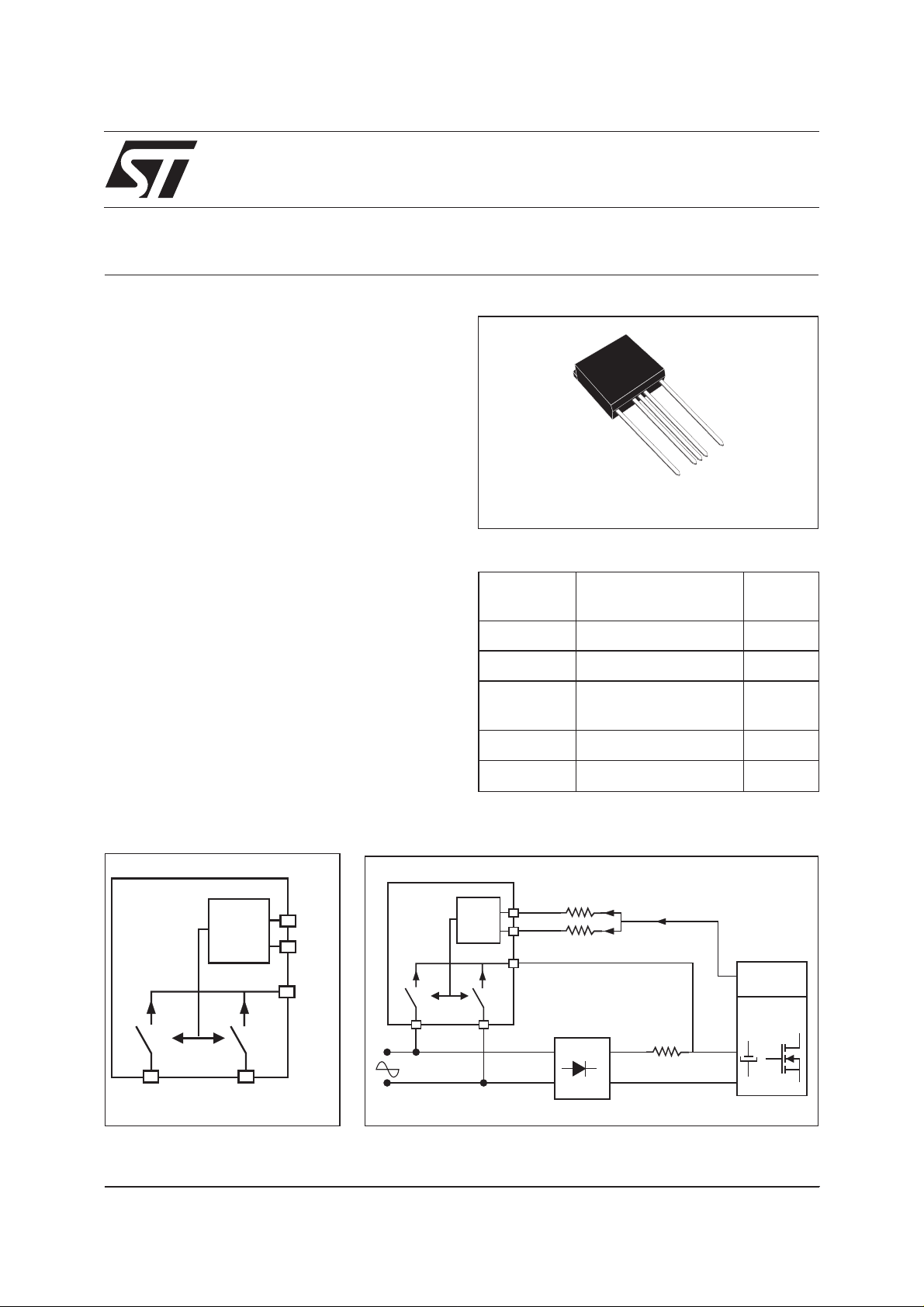
2
1
PENTAWATT HV2
(in line)
PIN OUT DESCRIPTION
Pin out
designation
L AC Line (switch1) 1
Pt1 Pilot of power switch 1 2
OUT Output
Pt2 Pilot of power switch 2 4
N AC Neutral (switch 2) 5
Description Position
(connected to Tab)
5
4
3
3
Fig. A1: Bloc Diagram.
STIL04-P5
DRIVER
NL
October 2002 - Ed: 3A
Pt 1
Pt 2
OUT
Fig. A2: Basic connection.
STIL04-P5
DRIVER
L
Pt 1
Pt 2
OUT
N
Ipt1
Ipt2
Ipt
Aux.
Supply
Main
converter
Ri
1/7
Page 2

STIL04-P5
Functional Description
The STIL04 isconnectedin parallel with the bridge diode and the inrush power resistor Ri (fig. A2). During
start up, the two unidirectional ASD™ power switches of the STIL04 are opened. The inrush current flows
through the diodes of the bridge and the external inrush power resistor Ri. Since the main converter turns
ON, the auxiliary power supply coupled with the main transformer, supplies the energy required to close
the two power switches of theSTIL04. At the normal state,the twobottom diodes of the bridgerectifier and
the two unidirectional switches of the STIL04 rectify the AC line current.
When the STIL04 isused with a PFC boostconverter, the inrush current circuitremains active after a short
ACline dropout(see fig.A5). Inthat configuration, since the AC line disappears,the PFCcontroller andthe
auxiliary power supply of the STIL turns OFF. The two switches of the STIL are opened. The output bulk
capacitorCb isdischarging and itis providingthe energy tothe mainconverter.When theAC line recovers,
the two switches remain opened and recharging inrush current of the capacitor Cb is deviated and limited
throughthe resistorRi. Whenthe capacitor ischarged, thePFC turnsON again and the twoswitches ofthe
STIL switch ON.
More details on the design and operation of the driver circuit of figure A5 can be found in the application
note “AN1600 - STIL: Inrush Current Limitation Device for Off-Line Power Converter”.
ABSOLUTE MAXIMUM RATINGS (Limiting value)
Symbol Parameter Value Unit
V
Dout
V
Rout
I
out(AV)
Repetitive forward (V
off-state voltage
Average on state current at the OUT terminal
) and reverse (V
Dout
Rout
)
Tj
Tj
(min)
(max)
to
Tj = 150°C
700 V
4A
(180° conduction angle for the internal power
switches)
I
out(RMS)
RMS on state current at the OUT terminal
Tj = 150°C
4.4 A
(180° conduction angle for the internal power
switches)
dI
I
TSM
2
t
I
out
Tstg
T
j
Non repetitive surge peak on-state current
(Tj initial = 25°C)
2
I
t value - rating for fusing tp = 10ms
Critical rate of rise of on state current
/dt
Ipt1 + Ipt2 = 20mA
Storage temperature range
Junction temperature range
tp = 10ms
sinusoidal
Tj = 25°C
Tj = 150°C
65 A
21 A
100 A/µs
-40 to +150 °C
0 to +150 °C
THERMAL PARAMETERS
Symbol Parameter Value Unit
Rth
Rth
(j-c)
(j-a)
Junction to case
Junction to ambient (minimum footprint)
2 °C/W
60
2
s
2/7
Page 3

STIL04-P5
ELECTRICAL CHARACTERISTICS
Symbol Parameter Test conditions Min. Typ. Max. Unit
V
V
dV
I
Rout
I
Rout
Ipt1
Ipt2
V
V
R
R
Vt0
+
D(pt1)
D(pt2)
(pt1)
(pt2)
Dout
(off)
(on)
Rd
V
F
Driver trigger current V
R
Dout
L
=30Ω
= 12V (DC)
tp = 380µs
Direct pilot trigger voltage V
R
Dout
L
=30Ω
= 12V (DC)
Peak reverse driver voltage Tj = 25°C
Dynamic voltage rising Linear slope up to
/dt
V
= 470V
Dout
Max reverse current without
driver current
Max reverse current with
driver current
Threshold direct voltage for
V
= 700V
Rout
Ipt1 = Ipt2 = open
V
= 400V
Dout
Ipt1 = Ipt2 = 10mA
I
= 4A Tj = 150°C
out(AV)
one power switch
Dynamic direct resistance for
I
= 4A Tj = 150°C
out(AV)
one power switch
Maximum instantaneous di-
I
out(AV)
= 4A Tj = 150°C
rect forward voltage drop for
one power switch
Tj = 0°C
Tj = 25°C
Tj = 0°C
Tj = 25°C
Tj = 150°C
Tj = 150°C
Tj = 25°C
Tj = 150°C
Tj = 150°C
12 20 mA
10
0.6 0.85 1 V
0.8 0.95
0.2 0.45
8V
500 V/µs
5µA
300 µA
300 µA
0.75 0.9 V
55 80 mΩ
1.1 1.4 V
Power losses calculations
When the input current is sinusoidal, the conducted power losses can be calculated by using the following
formula:
PVI R
=+
.
T out av d
0
()
(
I
out av
()
2
π
×
)
8
If the output average current is 4Amps, VT0and Rd of the electrical characteristics table can be used. For
differentoutput current pleaserefer tothe application noteAN1600 thatprovides guidelines toestimate the
correct values of VT0and Rd.
LIGHTNING SURGE IMMUNITY (IEC61000-4-5)
During lightning surge transient voltage across the AC line, over current and over voltage stress are appliedon allthe components of the powersupply. TheSTIL04 can sustain a maximumpeak surgecurrent of
500Aas defined by the combinewaveform generator (8/20µswaveform as shownin fig. A3 and A4).
Special recommendations for the lightning surge immunity:
1 - Check that the maximum peak surge current in the STIL stays below the limit specified above.
2 - Check that no over voltages are applied on the STIL and the bridge diode.
3 - In order to reduce the dynamic current stress (dI
/dt) through the structure of the STIL04, it is recom-
out
mended to connect a differential mode choke coil in front of the STIL and the bridge diode.
More details and design guidelines are provided in the application note “AN1600 - STIL: Inrush Current
Limitation Device for Off-Line Power Converter”.
3/7
Page 4

STIL04-P5
Fig. A3: Surge test condition.
STIL04-P5
L
DRIVER
N
Pt 1
Pt 2
IOUT
OUT
VOUT
IOUT
5Vdc
0
Combine
generator
Fig. A4: Surge current waveform.
0 Amps
Fig. A5: Basic connection with a PFC Boost preregulator.
Ri
1
5 µs
80A/Div
I
OUT
Ipeak=500A
1
by pass diode
Bridge
Diode
STIL04-P5
L
DRIVER
N
Pt 1
Pt 2
OUT
R1
R2
C0
C2
C1
PFC
Control
R
Vout
Cb
4/7
Page 5

STIL04-P5
Fig. 1-1: Non repetitive surge peak on-state cur-
rent (sinusoidal pulse) and corresponding value of
2
t.
I
I (A), I²t(A²s)
TSM
1000.0
I
TSM
100.0
10.0
tp(ms)
1.0
0.01 0.10 1.00 10.00
T initial=25°C
j
I²t
Fig. 2: Relative variation of driver trigger current
versus junction temperature (typical values).
Ipt1 or Ipt2 [Tj] / Ipt1 or Ipt2 [Tj = 25°C]
1.4
1.3
1.2
1.1
1.0
0.9
0.8
0.7
0.6
0.5
0.4
0.3
0.2
0 25 50 75 100 125 150
Tj(°C)
Fig. 1-2: Non repetitive surge peak on-state cur-
rent (sinusoidal pulse) and corresponding value of
2
t.
I
I (A), I²t(A²s)
TSM
1000.0
I
TSM
100.0
10.0
tp(ms)
1.0
0.01 0.10 1.00 10.00
T initial=150°C
j
I²t
Fig. 3: Relative variation of directpilot voltage versus junction temperature (typical values).
VDpt1 orVDpt2 [Tj] /VDpt1 orVDpt2 [Tj = 25°C]
1.2
1.1
1.0
0.9
0.8
0.7
0.6
0.5
0.4
0 25 50 75 100 125 150
Tj(°C)
Fig. 4: Relative variation of thermal impedance
junction to case versus pulse duration.
K = [Zth(j-c)/Rth(j-c)]
1.E+00
tp(s)
1.E-01
1.E-03 1.E-02 1.E-01 1.E+00
Fig. 5-1: Reverse current versus junction temper-
ature without driver current (typical values).
R(OUT)
I OFF(µA)
1.E+02
1.E+01
1.E+00
1.E-01
1.E-02
Tj(°C)
1.E-03
0 25 50 75 100 125 150
P & P open
t1 t2
V =700V
R(out)
5/7
Page 6

STIL04-P5
Fig. 5-2: Reverse current versus junction temper-
ature with driver current (typical values).
I ON(µA)
R(OUT)
100.0
I = I =10mA
pt1 pt2
V =400V
R(out)
10.0
Tj(°C)
1.0
0 25 50 75 100 125 150
Fig. 7-1: Peak forward voltage dropversus peak
forward output current for one power switch at
Tj = 25°C (typical and maximal values).
I (A)OUT
12
T=25°C
j
11
10
9
8
7
6
5
4
3
2
1
0
0.8 0.9 1.0 1.1 1.2 1.3 1.4 1.5 1.6 1.7
Typical
Maximum
V (V)F
Fig. 6: Forward voltage drop for one power switch
versus junction temperature at the peak forward
current(typical values).
F
V (V)
1.20
1.16
1.12
1.08
1.04
I =6.3A
out(peak)
Tj(°C)
1.00
0 25 50 75 100 125 150
Fig. 7-2: Peak forward voltage dropversus peak
forward output current for one power switch at
Tj= 150°C (typicalvalues andmaximal values).
I (A)OUT
12
T=150°C
j
11
10
9
8
7
6
5
4
3
2
1
0
0.7 0.8 0.9 1.0 1.1 1.2 1.3 1.4 1.5 1.6 1.7
Typical
Maximum
V (V)F
Fig. 8: Relative variation of dV/dt immunity versus
junction temperature (typical values).
DOUT DOUT
dV [Tj] / dV [Tj=150°C]
20
18
16
14
12
10
8
6
4
2
0
25 50 75 100 125 150
Tj(°C)
6/7
V =470V
Dout
Page 7

PACKAGE MECHANICAL DATA
PENTAWATT HV2
STIL04-P5
A
C
H2
L7
REF. DIMENSIONS
Millimeters Inches
Min. Max. Min. Max.
A 4.19 4.70 0.165 0.185
C 1.14 1.40 0.044 0.055
L6
D 2.5 2.72 0.098 0.107
E 0.38 0.51 0.015 0.020
D
L3
F 0.66 0.82 0.026 0.032
G 2.54 Typ. 0.10 Typ.
G2 7.62 Typ. 0.30 Typ.
E
H2 10.04 10.29 0.395 0.405
L3 23.5 Typ. 0.925 Typ.
L6 9.90 10.16 0.389 0.400
G
G2
F
L7 1.52 Typ. 0.059 Typ.
Order code Marking Package Weight Delivery mode Base qty
STIL04-P5 STIL04 PENTAWATT
1.9 g. Tube 50
HV2 (in line)
Informationfurnished is believed to be accurateand reliable. However, STMicroelectronics assumes noresponsibility for the consequences of
useof such information nor for any infringement ofpatents or other rights of third parties which mayresult from its use. No license is grantedby
implication or otherwise under any patent or patent rights of STMicroelectronics. Specifications mentioned in this publication are subject to
change without notice. This publication supersedes and replaces all information previously supplied.
STMicroelectronics products are not authorized for use as critical components in life support devices or systems without express written approval of STMicroelectronics.
The ST logo is a registered trademark of STMicroelectronics
© 2002 STMicroelectronics - Printed in Italy - All rights reserved.
STMicroelectronics GROUP OF COMPANIES
Australia - Brazil - Canada - China - Finland - France - Germany
Hong Kong - India - Israel - Italy - Japan - Malaysia - Malta - Morocco - Singapore
Spain - Sweden - Switzerland - United Kingdom - United States.
http://www.st.com
7/7
 Loading...