

Page 1
STH6N100
STH6N100FI
N - CHANNEL ENHANCEMENT MODE
POWER MOS TRANSISTOR
TYPE V
STH6N100
STH6N100FI
■ TYPICAL R
■ AVALANCHE RUGGED TECHNOLOGY
■ 100% AVALANCHE TESTED
■ REPETITIVE AVALANCHE DATA AT 100
■ LOW INPUT CAPACITANCE
■ LOW GATE CHARGE
■ APPLICATION ORIENTED
DS(on)
DSS
1000 V
1000 V
= 1.75 Ω
R
DS(on)
<2Ω
<2Ω
I
D
6A
3.7 A
o
C
CHARACTERIZATION
APPLICATIONS
■ HIGH CURRENT, HIGH SPEED SWITCHING
■ SWITCH MODE POWERSUPPLIES (SMPS)
■ CONSUMER AND INDUSTRIAL LIGHTING
■ DC-AC INVERTERS FOR WELDING
EQUIPMENT AND UNINTERRUPTIBLE
POWER SUPPLY (UPS)
3
2
1
1
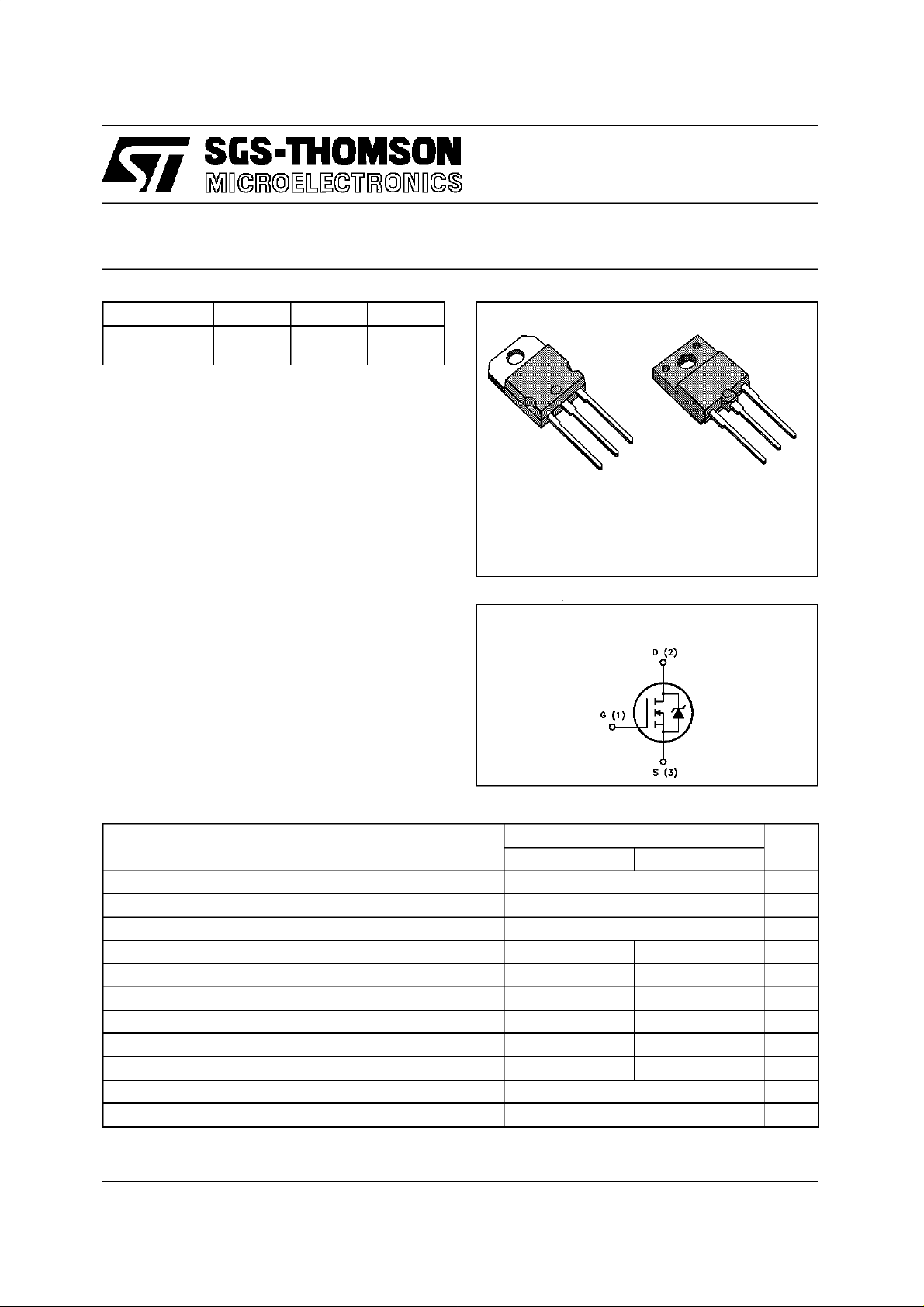
TO-218 ISOWATT218
INTERNAL SCHEMATIC DIAGRAM
3
2
ABSOLUTE MAXIMUM RATINGS
Symb o l Paramet er Val u e Unit
ST H6N100 STH6N100
V
V
V
I
DM
P
V
T
(•) Pulsewidth limited bysafe operating area
December 1996
Drain - s ource Voltage (VGS= 0) 1000 V
DS
Drain- gate Voltage (RGS=20kΩ) 1000 V
DGR
Gate-source Voltage ± 20 V
GS
Drain Current (continuous) at Tc=25oC63.7A
I
D
Drain Current (continuous) at Tc=100oC3.7 2.3A
I
D
(•) Drain Current (pulsed) 24 24 A
Total Di ssipation at Tc=25oC 180 70 W
tot
Derat ing Factor 1.44 0.56 W/
Ins ulation Withs t and Voltage (DC) 4000 V
ISO
St or a ge Tem perature -65 to 150
stg
Max. Operating Junction Temperature 150
T
j
o
o
o
C
C
C
1/10
Page 2
STH6N100/FI
THERMAL DATA
TO-218 ISOW ATT 218
R
thj-case
R
thj-amb
R
thc-sink
T
AVALANCHE CHARACTERISTICS
Symbol Parameter Max Value Uni t
I
AR
E
E
I
AR
Thermal Resistance Junction - cas e M ax 0.69 1.78
Thermal Resistance Junction- ambient Max
Thermal Resistance Case-sink Typ
Maximum Lead T emperature For Soldering Purpose
l
Avalanc h e Cu rr ent , Repet itive or Not-R ep et itive
(pulse width limited by Tjmax, δ <1%)
Single Pul se Avalanche Ener gy
AS
(starti ng T
Repetitive Avalanc he Energ y
AR
=25oC, ID=IAR,VDD=25V)
j
(pulse width limited by Tjmax, δ <1%)
Avalanc h e Cu rr ent , Repet itive or Not-R ep et itive
(Tc= 100oC, pulse width limited by Tjmax, δ <1%)
30
0.1
300
6A
850 mJ
16 mJ
3.7 A
o
C/W
o
C/W
o
C/W
o
C
ELECTRICAL CHARACTERISTICS (T
=25oC unless otherwise specified)
case
OFF
Symbol Parameter Test Condi tions Min. Typ. Max. Unit
V
(BR)DSS
Drain - s ource
ID=250µAVGS= 0 1000 V
Break d own Volta ge
I
DSS
I
GSS
Zer o Gate Volt age
Drain Current (VGS=0)
Gat e- body Leak age
Current (V
DS
=0)
VDS=MaxRating
VDS= Max Rating x 0 .8 Tc=125oC
= ± 20 V ± 100 nA
V
GS
25
250
ON (∗)
Symbol Parameter Test Condi tions Min. Typ. Max. Unit
V
GS(th)
R
DS(on)
Gate Threshold Voltage VDS=VGSID=250µA234V
St at ic Drain-s our ce O n
VGS=10V ID=3A 1.75 2 Ω
Resistance
I
D(on)
On State Drain Current VDS>I
D(on)xRDS(on)max
6A
VGS=10V
DYNAMIC
Symbol Parameter Test Condi tions Min. Typ. Max. Unit
(∗)Forward
g
fs
Tr ansconductance
C
C
C
Input Capacitance
iss
Out put Capacitance
oss
Reverse Transfer
rss
Capacitance
VDS>I
D(on)xRDS(on)maxID
=3A 4 5.5 S
VDS=25V f=1MHz VGS= 0 2150
260
105
2800
330
130
µA
µA
pF
pF
pF
2/10
Page 3
STH6N100/FI
ELECTRICAL CHARACTERISTICS (continued)
SWITCHING ON
Symbol Parameter Test Condi tions Min. Typ. Max. Unit
t
d(on)
(di/dt)
Q
Q
Q
Turn-on T im e
t
Rise Time
r
Turn-on C urrent S lope VDD=800V ID=6A
on
Total Gate Charge
g
Gat e- Source Charge
gs
Gate-Drain Charge
gd
SWITCHING OFF
Symbol Parameter Test Condi tions Min. Typ. Max. Unit
t
r(Voff)
t
Off -voltage R ise Time
t
Fall Time
f
Cross-over Time
c
SOURCE DRAIN DIODE
VDD=500V ID=3A
RG=50 Ω VGS=10V
70
21090280
(see test circuit, figure 3)
180 A/µs
RG=50Ω VGS=10V
(see test circuit, figure 5)
VDD= 400 V ID=6A VGS=10V 125
15
55
VDD=800V ID=6A
RG=50 Ω VGS=10V
(see test circuit, figure 5)
190
50
265
150 nC
250
65
345
ns
ns
nC
nC
ns
ns
ns
Symbol Parameter Test Condi tions Min. Typ. Max. Unit
I
I
SDM
SD
Source-drain Current
(•)
Source-drain Current
6
24
(pulsed)
V
(∗) F or ward O n Voltage ISD=6A VGS=0 2 V
SD
t
Reverse Recovery
rr
Time
Q
Reverse Recovery
rr
ISD=6A di/dt=100A/µs
VDD= 100 V Tj=150oC
(see test circuit, figure 5)
1100
31
Charge
I
RRM
Reverse Recovery
57
Current
(∗) Pulsed:Pulse duration = 300 µs, dutycycle 1.5 %
(•) Pulse widthlimited by safeoperating area
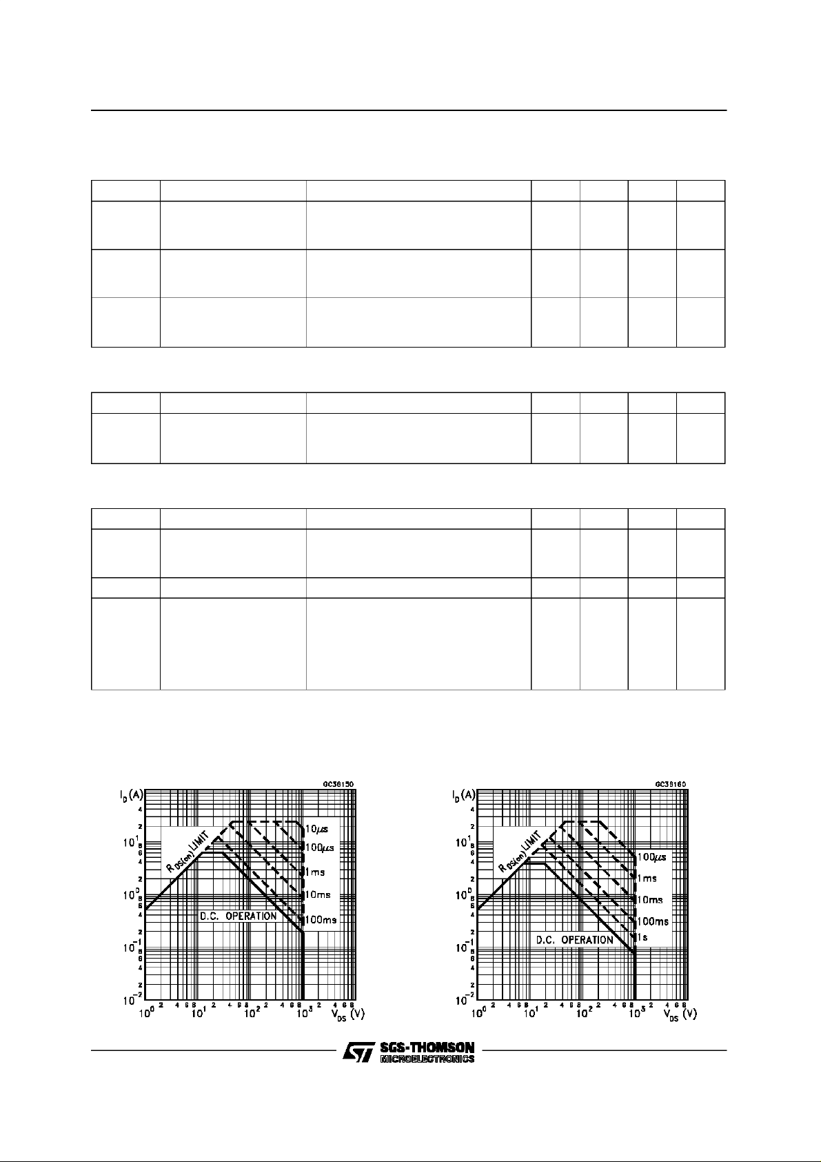
Safe Operating Areas For TO-218 Safe Operating Areas For ISOWATT218
A
A
ns
µC
A
3/10
Page 4

STH6N100/FI
Thermal ImpedeanceFor TO-218
Derating Curve For TO-218
Thermal Impedance For ISOWATT218
Derating Curve For ISOWATT218
Output Characteristics
4/10
Transfer Characteristics
Page 5

Transconductance Static Drain-source On Resistance
Gate Charge vs Gate-sourceVoltage Capacitance Variations
STH6N100/FI
Temperature
Normalized On Resistance vs TemperatureNormalized Gate Threshold Voltage vs
5/10
Page 6

STH6N100/FI
Turn-on Current Slope Turn-off Drain-source Voltage Slope
Cross-over Time Switching Safe Operating Area
Accidental Overload Area Source-drain Diode ForwardCharacteristics
6/10
Page 7

STH6N100/FI
Fig. 1: Unclamped Inductive Load Test Circuits
Fig. 3: Switching Times Test Circuits For
Resistive Load
Fig. 2: Unclamped Inductive Waveforms
Fig. 4: Gate Charge Test Circuit
Fig. 5: Test Circuit For Inductive Load Switching
And Diode Reverse Recovery Time
7/10
Page 8

STH6N100/FI
TO-218 (SOT-93) MECHANICAL DATA
DIM.
MIN. TYP. MAX. MIN. TYP. MAX.
A 4.7 4.9 0.185 0.193
C 1.17 1.37 0.046 0.054
D 2.5 0.098
E 0.5 0.78 0.019 0.030
F 1.1 1.3 0.043 0.051
G 10.8 11.1 0.425 0.437
H 14.7 15.2 0.578 0.598
L2 – 16.2 – 0.637
L3 18 0.708
L5 3.95 4.15 0.155 0.163
L6 31 1.220
R – 12.2 – 0.480
Ø 4 4.1 0.157 0.161
mm inch
E
A
C
L5
D
L6
L3
L2
H
G
Ø
F
R
123
P025A
8/10
Page 9

ISOWATT218 MECHANICAL DATA
STH6N100/FI
DIM.
mm inch
MIN. TYP. MAX. MIN. TYP. MAX.
A 5.35 5.65 0.210 0.222
C 3.3 3.8 0.130 0.149
D 2.9 3.1 0.114 0.122
D1 1.88 2.08 0.074 0.081
E 0.45 1 0.017 0.039
F 1.05 1.25 0.041 0.049
G 10.8 11.2 0.425 0.441
H 15.8 16.2 0.622 0.637
L1 20.8 21.2 0.818 0.834
L2 19.1 19.9 0.752 0.783
L3 22.8 23.6 0.897 0.929
L4 40.5 42.5 1.594 1.673
L5 4.85 5.25 0.190 0.206
L6 20.25 20.75 0.797 0.817
M 3.5 3.7 0.137 0.145
N 2.1 2.3 0.082 0.090
U 4.6 0.181
L3
N
E
A
D
C
L5
M
H
L2
L6
L1
D1
L4
F
U
G
123
P025C
9/10
Page 10

STH6N100/FI
Information furnished is believed to be accurate and reliable. However, SGS-THOMSON Microelectronics assumes no responsability for the
consequences of use of such informationnor for any infringement of patents or other rights of third parties which mayresults fromits use. No
licenseis granted by implication orotherwise under any patentor patentrights of SGS-THOMSONMicroelectronics. Specifications mentioned
in thispublication are subject to change withoutnotice. Thispublication supersedes andreplacesall informationpreviously supplied.
SGS-THOMSONMicroelectronicsproducts are notauthorized for use ascriticalcomponents in lifesupportdevices or systems withoutexpress
writtenapproval of SGS-THOMSON Microelectonics.
1996 SGS-THOMSON Microelectronics -Printed in Italy- AllRightsReserved
Australia- Brazil -Canada -China- France- Germany - HongKong- Italy- Japan- Korea- Malaysia - Malta - Morocco- The Netherlands -
Singapore- Spain - Sweden - Switzerland-Taiwan - Thailand- UnitedKingdom - U.S.A
SGS-THOMSONMicroelectronics GROUP OF COMPANIES
.
10/10
 Loading...