

Page 1
STH60N10/FI
STW60N10
N - CHANNEL ENHANCEMENT MODE
POWER MOS TRANSISTOR
TYPE V
STH 60N10
STH 60N10FI
STW60N10
■ TYPICAL R
■ AVALANCHE RUGGED TECHNOLOGY
■ 100% AVALANCHE TESTED
■ REPETITIVE AVALANCHE DATA AT 100
■ LOW GATE CHARGE
■ VERY HIGH CURRENT CAPABILITY
o
■ 175
■ APPLICATION ORIENTED
C OPERATING TEMPERATURE
DS(on)
DSS
100 V
100 V
100 V
= 0.02 Ω
R
DS(on)
< 0.025 Ω
< 0.025 Ω
< 0.025 Ω
I
D
60 A
36 A
60 A
o
C
CHARACTERIZATION
APPLICATIONS
■ HIGH CURRENT, HIGH SPEED SWITCHING
■ SOLENOID AND RELAY DRIVERS
■ REGULATORS
■ DC-DC & DC-AC CONVERTERS
■ MOTOR CONTROL, AUDIO AMPLIFIERS
■ AUTOMOTIVE ENVIRONMENT (INJECTION,
ABS, AIR-BAG, LAMPDRIVERS, Etc.)
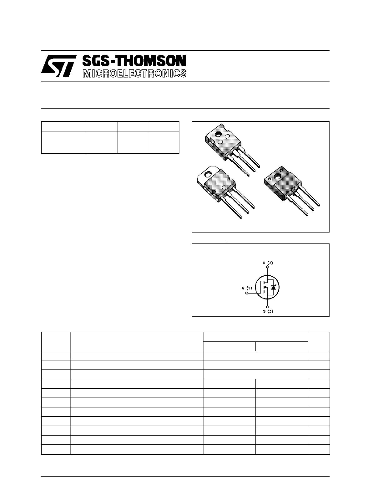
TO-247
3
2
1
3
2
TO-218 ISOWATT218
1
INTERNAL SCHEMATIC DIAGRAM
3
2
1
ABSOLUTE MAXIMUM RATINGS
Symb o l Paramet er Val u e Unit
STH/STW60N10 STH6 0N10FI
V
V
V
I
DM
P
V
T
(•) Pulsewidth limited bysafe operating area
May 1993
Drain - s ource Voltage (VGS=0) 100 V
DS
Drain- gate Voltage (RGS=20kΩ)100V
DGR
Gate-source Voltage ± 20 V
GS
Drain Current (continuous) at Tc=25oC6036A
I
D
Drain Current (continuous) at Tc=100oC42 22A
I
D
(•) Drain Current (pulsed) 240 240 A
Total Di ssipation at Tc=25oC 200 70 W
tot
Derat ing Factor 1.33 0.56 W/
Ins ulation Withs t and Voltage (DC) 4000 V
ISO
St or a ge Tem perature -65 to 175 -65 to 1 50
stg
Max. Operating Junction Temperature 175 1 50
T
j
o
o
o
C
C
C
1/11
Page 2
STH60N10/FI STW60N10
THERMAL DATA
TO - 218/ TO-247 IS OWATT218
R
thj-case
R
thj-amb
R
thc-sink
T
AVALANCHE CHARACTERISTICS
Symbol Parameter Max Value Uni t
I
AR
E
E
I
AR
Thermal Resistance Junction - cas e Max 0.75 1.79
Thermal Resistance Junction- ambient Max
Thermal Resistance Case-sink Typ
Maximum Lead T emperature For Soldering Purpose
l
Avalanc h e Cu rr ent , Repet itive or Not-R ep et itive
(pulse width limited by Tjmax, δ <1%)
Single Pul se Avalanche Ener gy
AS
(starti ng T
Repetitive Avalanc he Energ y
AR
=25oC, ID=IAR,VDD=25V)
j
(pulse width limited by Tjmax, δ <1%)
Avalanc h e Cu rr ent , Repet itive or Not-R ep et itive
(Tc= 100oC, pulse width limited by Tjmax, δ <1%)
30
0.1
300
60 A
720 mJ
180 mJ
37 A
o
C/W
o
C/W
o
C/W
o
C
ELECTRICAL CHARACTERISTICS (T
=25oC unless otherwise specified)
case
OFF
Symbol Parameter Test Co ndition s Min. Typ. Max. Unit
V
(BR)DSS
Drain - s ource
ID=250µAVGS= 0 100 V
Break d own Volta ge
I
DSS
I
GSS
Zer o Gate Volt age
Drain Current (VGS=0)
Gat e- body Leak age
Current (V
DS
=0)
VDS=MaxRating
VDS= Max Rating x 0 .8 Tc=125oC
= ± 20 V ± 100 nA
V
GS
250
1000µAµA
ON (∗)
Symbol Parameter Test Co ndition s Min. Typ. Max. Unit
V
GS(th)
R
DS(on)
I
D(on)
Gate Threshold Voltage VDS=VGSID=250µA22.94V
St at ic Drain-s our ce O n
Resistance
On State Drain Current VDS>I
VGS=10V ID=30A
VGS=10V ID=30A Tc= 100oC
D(on)xRDS(on)max
0.02 0.025
0.05
60 A
VGS=10V
DYNAMIC
Symbol Parameter Test Co ndition s Min. Typ. Max. Unit
(∗)Forward
g
fs
Tr ansconductance
C
C
C
Input Capacitance
iss
Out put Capacitance
oss
Reverse Transfer
rss
Capacitance
VDS>I
D(on)xRDS(on)maxID
=30A 25 35 S
VDS=25V f=1MHz VGS= 0 4000
1100
250
5000
1400
350
Ω
Ω
pF
pF
pF
2/11
Page 3
STH60N10/FI STW60N10
ELECTRICAL CHARACTERISTICS (continued)
SWITCHING ON
Symbol Parameter Test Co ndition s Min. Typ. Max. Unit
t
d(on)
(di/dt)
Q
Q
Q
Turn-on T im e
t
Rise Time
r
Turn-on C urrent S lope VDD=80V ID=60A
on
Total Gate Charge
g
Gat e- Source Charge
gs
Gate-Drain Charge
gd
SWITCHING OFF
Symbol Parameter Test Co ndition s Mi n. Ty p. Max. Unit
t
r(Voff)
t
Off -voltage R ise Time
t
Fall Time
f
Cross-over Time
c
SOURCE DRAIN DIODE
VDD=80V ID=30A
RG=50 Ω VGS=10V
90
270
(see test circuit, figure 3)
270 A/µs
RG=50 Ω VGS=10V
(see test circuit, figure 5)
VDD=80V ID=30A VGS=10V 120
16
60
VDD=80V ID=60A
RG=50 Ω VGS=10V
(see test circuit, figure 5)
200
210
410
130
380
170 nC
280
290
570
ns
ns
nC
nC
ns
ns
ns
Symbol Parameter Test Co ndition s Mi n. Ty p. Max. Unit
I
I
SDM
SD
Source-drain Current
(•)
Source-drain Current
60
240
(pulsed)
V
(∗) Forward On Volt age ISD=60A VGS=0 1.6 V
SD
t
Reverse Recovery
rr
Time
Q
Reverse Recovery
rr
ISD= 60 A di/dt = 100 A/µs
VDD=30V Tj=150oC
(see test circuit, figure 5)
180
1
Charge
I
RRM
Reverse Recovery
11
Current
(∗) Pulsed:Pulse duration = 300 µs, dutycycle 1.5 %
(•) Pulse widthlimited by safeoperating area
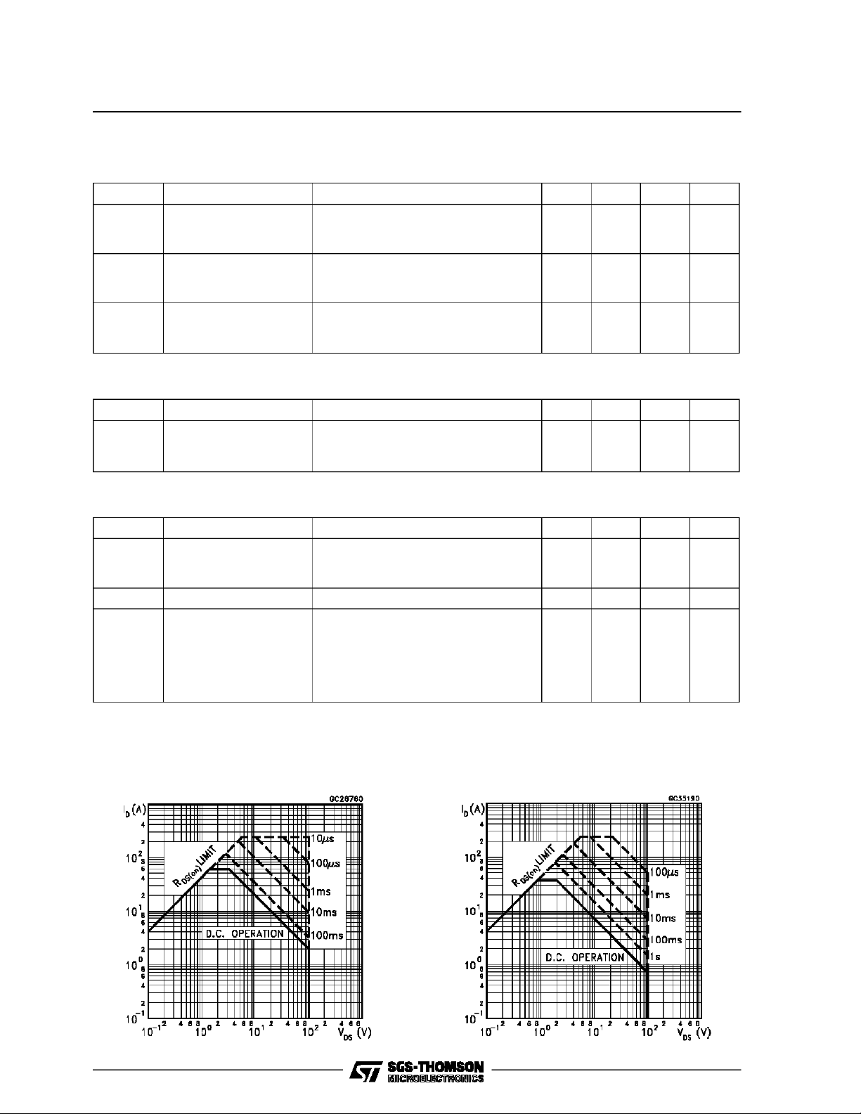
Safe Operating Areas For TO-218 and TO-247 Safe Operating Areas For ISOWATT218
A
A
ns
µC
A
3/11
Page 4
STH60N10/FI STW60N10
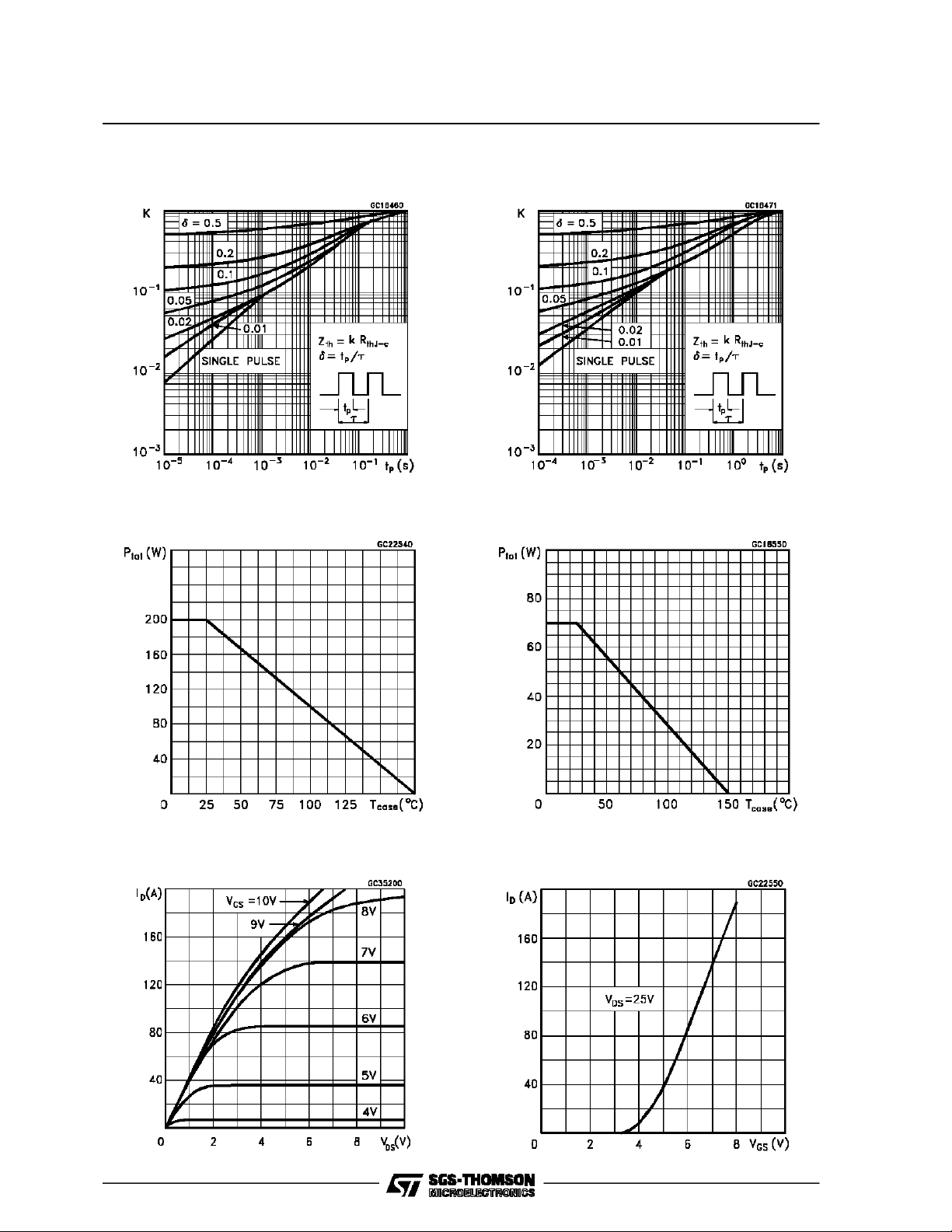
Thermal ImpedeanceFor TO-218 and TO-247
Derating Curve For TO-218 and TO-247
Thermal Impedance For ISOWATT218
Derating Curve For ISOWATT218
Output Characteristics
4/11
Transfer Characteristics
Page 5

STH60N10/FI STW60N10
Transconductance Static Drain-source On Resistance
Gate Charge vs Gate-sourceVoltage Capacitance Variations
Temperature
Normalized On Resistance vs TemperatureNormalized Gate Threshold Voltage vs
5/11
Page 6

STH60N10/FI STW60N10
Turn-on Current Slope Turn-off Drain-source Voltage Slope
Cross-over Time Switching Safe Operating Area
Accidental Overload Area Source-drain Diode ForwardCharacteristics
6/11
Page 7

STH60N10/FI STW60N10
Fig. 1: Unclamped Inductive Load Test Circuits
Fig. 3: Switching Times Test Circuits For
Resistive Load
Fig. 2: Unclamped Inductive Waveforms
Fig. 4: Gate Charge Test Circuit
Fig. 5: Test Circuit For Inductive Load Switching
And Diode Reverse Recovery Time
7/11
Page 8

STH60N10/FI STW60N10
TO-247 MECHANICAL DATA
DIM.
MIN. TYP. MAX. MIN. TYP. MAX.
A 4.7 5.3 0.185 0.208
A1 2.87 0.113
A2 1.5 2.5 0.059 0.098
b 1 1.4 0.039 0.055
b1 2.25 0.088
b2 3.05 3.43 0.120 0.135
C 0.4 0.8 0.015 0.031
D 20.4 21.18 0.803 0.833
e 5.43 5.47 0.213 0.215
E 15.3 15.95 0.602 0.628
L 15.57 0.613
L1 3.7 4.3 0.145 0.169
Q 5.3 5.84 0.208 0.230
ØP 3.5 3.71 0.137 0.146
mm inch
8/11
C
A
b1
A1
b
e
b2
A2
Q
D
L1
L
ø
E
Page 9

STH60N10/FI STW60N10
TO-218 (SOT-93) MECHANICAL DATA
DIM.
MIN. TYP. MAX. MIN. TYP. MAX.
A 4.7 4.9 0.185 0.193
C 1.17 1.37 0.046 0.054
D 2.5 0.098
E 0.5 0.78 0.019 0.030
F 1.1 1.3 0.043 0.051
G 10.8 11.1 0.425 0.437
H 14.7 15.2 0.578 0.598
L2 – 16.2 – 0.637
L3 18 0.708
L5 3.95 4.15 0.155 0.163
L6 31 1.220
R – 12.2 – 0.480
Ø 4 4.1 0.157 0.161
mm inch
E
A
C
L5
D
L6
L3
L2
H
G
Ø
F
R
123
P025A
9/11
Page 10

STH60N10/FI STW60N10
ISOWATT218 MECHANICAL DATA
DIM.
mm inch
MIN. TYP. MAX. MIN. TYP. MAX.
A 5.35 5.65 0.210 0.222
C 3.3 3.8 0.130 0.149
D 2.9 3.1 0.114 0.122
D1 1.88 2.08 0.074 0.081
E 0.45 1 0.017 0.039
F 1.05 1.25 0.041 0.049
G 10.8 11.2 0.425 0.441
H 15.8 16.2 0.622 0.637
L1 20.8 21.2 0.818 0.834
L2 19.1 19.9 0.752 0.783
L3 22.8 23.6 0.897 0.929
L4 40.5 42.5 1.594 1.673
L5 4.85 5.25 0.190 0.206
L6 20.25 20.75 0.797 0.817
M 3.5 3.7 0.137 0.145
N 2.1 2.3 0.082 0.090
U 4.6 0.181
L3
N
E
A
D
C
L5
M
H
L2
L6
L1
D1
L4
F
U
G
123
P025C
10/11
Page 11

STH60N10/FI STW60N10
Information furnished isbelieved to be accurateand reliable. However, SGS-THOMSONMicroelectronics assumes no responsability for the
consequences of use of suchinformation nor for any infringementof patents orother rights of third parties whichmay results from its use. No
license isgrantedby implicationor otherwiseunderany patentor patentrights ofSGS-THOMSON Microelectronics.Specificationsmentioned
in this publicationare subjectto change without notice.This publication supersedes and replacesall information previouslysupplied.
SGS-THOMSON Microelectronicsproducts are notauthorizedforuse ascriticalcomponentsin lifesupportdevices orsystemswithoutexpress
written approvalof SGS-THOMSON Microelectonics.
1994 SGS-THOMSONMicroelectronics - All Rights Reserved
Australia - Brazil- France - Germany - Hong Kong - Italy - Japan - Korea - Malaysia - Malta -Morocco - The Netherlands-
Singapore -Spain - Sweden- Switzerland -Taiwan - Thailand - United Kingdom -U.S.A
SGS-THOMSON Microelectronics GROUP OF COMPANIES
11/11
 Loading...