

Page 1
1/9July 2000
STGD7NB60H
N-CHANNEL 7A - 600V - DPAK
PowerMESH™ IGBT
■ HIGH INPUT IMPEDANCE
■ LOW ON-VOLTAGE DROP (V
cesat
)
■ OFF LOSSES INCLUDE TAIL CURRENT
■ LOW GATE CHARGE
■ HIGH CURRENT CAPABILITY
■ VERY HIGH FREQUENCY OPERATION
■ CO-PACKAGED WITH TURBOSWITCHT
■ TYPICAL SHORT CIRCUIT WITHSTAND TIME
5MICROS S-family, 4 micro H family
■ ANTIPARALLEL DIODE
DESCRIPTION
Using the latest high voltage technology based on a
patented strip layout, STMicroelectronics has designed an advanced family of IGBTs, the Power-
MESH™ IGBTs, with outstanding perfomances.
The suffix "H" identifies a f amily optimized f or high
frequency applications (up to 50kHz)in order to
achieve very high switching performances (reduced
tfall) mantaining a low voltage drop.
APPLICATIONS
■ HIGH FREQUENCY MOTOR CONTROLS
■ SMPS and PFC IN BOTH HARD SWITCH AND
RESONANT TOPOLOGIES
ABSOLUTE MAXIMUM RATINGS
TYPE V
CES
V
CE(sat)
I
C
STD7NB60H 600 V < 2.8 V7 A
Symbol Parameter Value Unit
V
CES
Collector-Em itter Voltage (VGS = 0)
600 V
V
ECR
Emitter-Colle ctor Voltage 20 V
V
GE
Gate-Emitter Voltage ± 20 V
I
C
Collector Current (continuos) at TC = 25°C
14 A
I
C
Collector Current (continuos) at TC = 100°C
7A
I
CM
(■)
Collector Current (pulsed) 56 A
P
TOT
Total Dissipation at TC = 25°C
55 W
Derating Factor 0.44 W/°C
T
stg
Storage Temperature –65 to 150 °C
T
j
Max. Operating Junction Temperature 150 °C
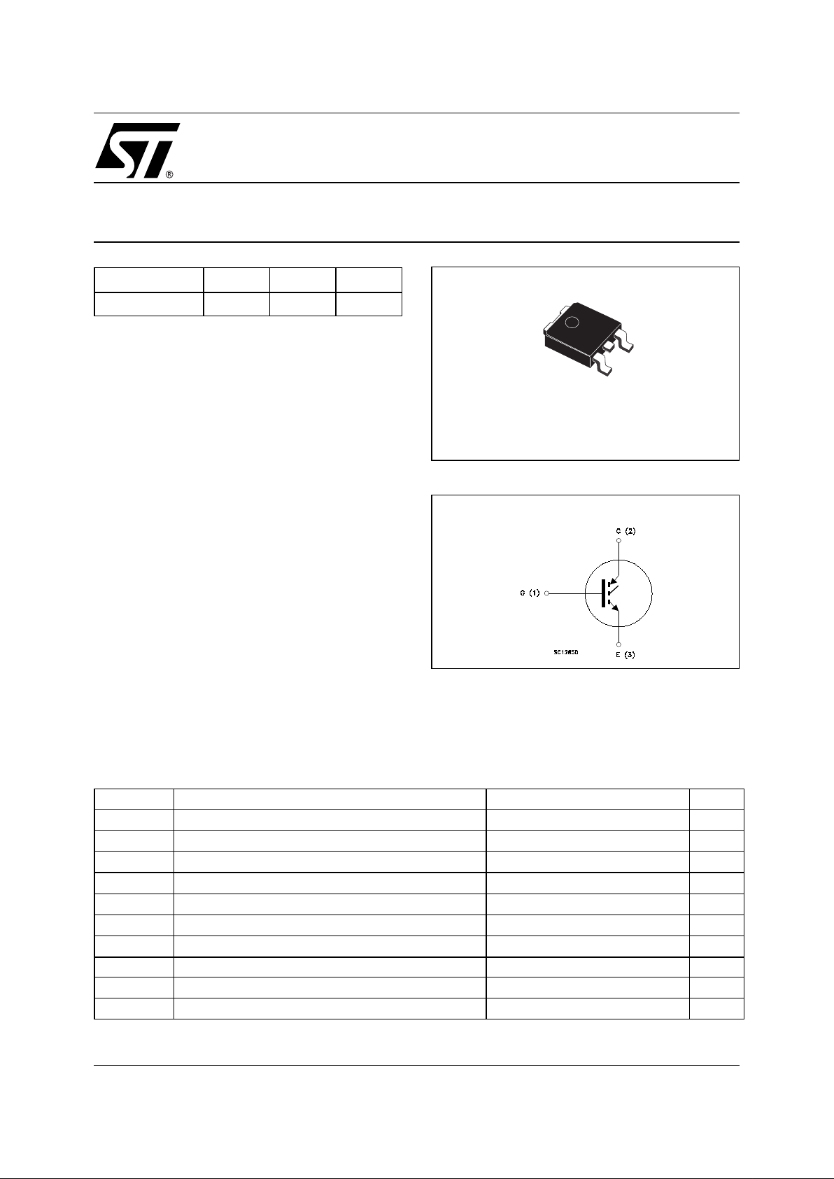
DPAK
1
3
INTERNAL SCHEMATIC DIAGRAM
Page 2

STGD7NB60H
2/9
THERMA L D ATA
ELECTRICAL CHARACTERISTICS (TCASE = 25 °C UNLESS OTHERWISE SPECIFIED)
OFF
ON
(1)
DYNAMIC
SWITCHING ON
Rthj-case Thermal Resistance Junction-case Max 2.27 °C/W
Rthj-amb Thermal Resistance Junction-ambient Max 100 °C/W
Rthc-sink Thermal Resistance Case-sink Typ 1.5 °C/W
Symbol Parameter Test Conditions Min. Typ. Max. Unit
V
BR(CES)
Collectro-Emitter Breakdown
Voltage
IC = 250 µA, VGE = 0 600 V
I
CES
Collector cut-off
(V
GE
= 0)
V
CE
= Max Rating, TC = 25 °C
10 µA
VCE = Max Rating, TC = 125 °C
100 µA
I
GES
Gate-Emitter Leakage
Current (V
CE
= 0)
V
GE
= ± 20V , VCE = 0 ±100 nA
Symbol Parameter Test Conditions Min. Typ. Max. Unit
V
GE(th)
Gate Threshold Voltage
V
CE
= VGE, IC = 250µA
35V
V
CE(sat)
Collector-Emitter Saturation
Voltage
VGE = 15V, IC = 7 A
2.3 2.8 V
VGE = 15V, IC = 7 A, Tj =125°C
1.9 V
Symbol Parameter Test Conditions Min. Typ. Max. Unit
g
fs
Forward Transconductance
V
CE
= 25 V , IC=3 A
3.5 5 S
C
ies
Input Capacitance
V
CE
= 25V, f = 1 MHz, VGE = 0
560 pF
C
oes
Output Capacitance 68 pF
C
res
Reverse Transfer
Capacitance
15 pF
Q
g
Q
ge
Q
gc
Total Gate Charge
Gate-Emitter Charge
Gate-Collector Charge
V
CE
= 480V, IC = 7 A,
V
GE
= 15V
42
7.9
17.6
55 nC
nC
nC
I
CL
Latching Current V
clamp
= 480 V , Tj = 150°C
RG = 10 Ω
28 A
Symbol Parameter Test Conditions Min. Typ. Max. Unit
t
d(on)
t
r
Turn-on Delay Time
Rise Time
V
CC
= 480 V, IC = 7 A
RG=10Ω , VGE = 15 V
15
48
ns
ns
(di/dt)
on
Eon
Turn-on Current Slope
Turn-on Switching Losses
V
CC
= 480 V, IC = 7 A RG=10Ω
V
GE
= 15 V,Tj = 125°C
160
70
A/µs
µJ
Page 3
3/9
STGD7NB60H
ELECTRICAL CHARACTERISTICS (CONTINUED)
SWITCHING OFF
Note: 1. Pulsed: Pu l se duration = 300 µs, duty cycle 1. 5 %.
2. Pulse width li mited by max. junction temp erature.
(**)Losses in clude Also the T ai l (Jedec Standardization)
Symbol Parameter Test Conditions Min. Typ. Max. Unit
t
c
Cross-over Time
V
cc
= 480 V, IC = 7 A,
R
GE
= 10 Ω , VGE = 15 V
85 ns
t
r(Voff
)
Off Voltage Rise Time 20 ns
td(
off
)
Delay Time 75 ns
t
f
Fall Time 70 ns
E
off
(**)
Turn-off Switching Loss 85
µJ
E
ts
Total Switching Loss 130
µJ
t
c
Cross-over Time
V
cc
= 480 V, IC = 3 A,
R
GE
= 10 Ω , VGE = 15 V
Tj = 125 °C
150 ns
t
r(Voff
)
Off Voltage Rise Time 50 ns
td(
off
)
Delay Time 110 ns
t
f
Fall Time 110 ns
E
off
(**)
Turn-off Switching Loss 220
µJ
E
ts
Total Switching Loss 290
µJ
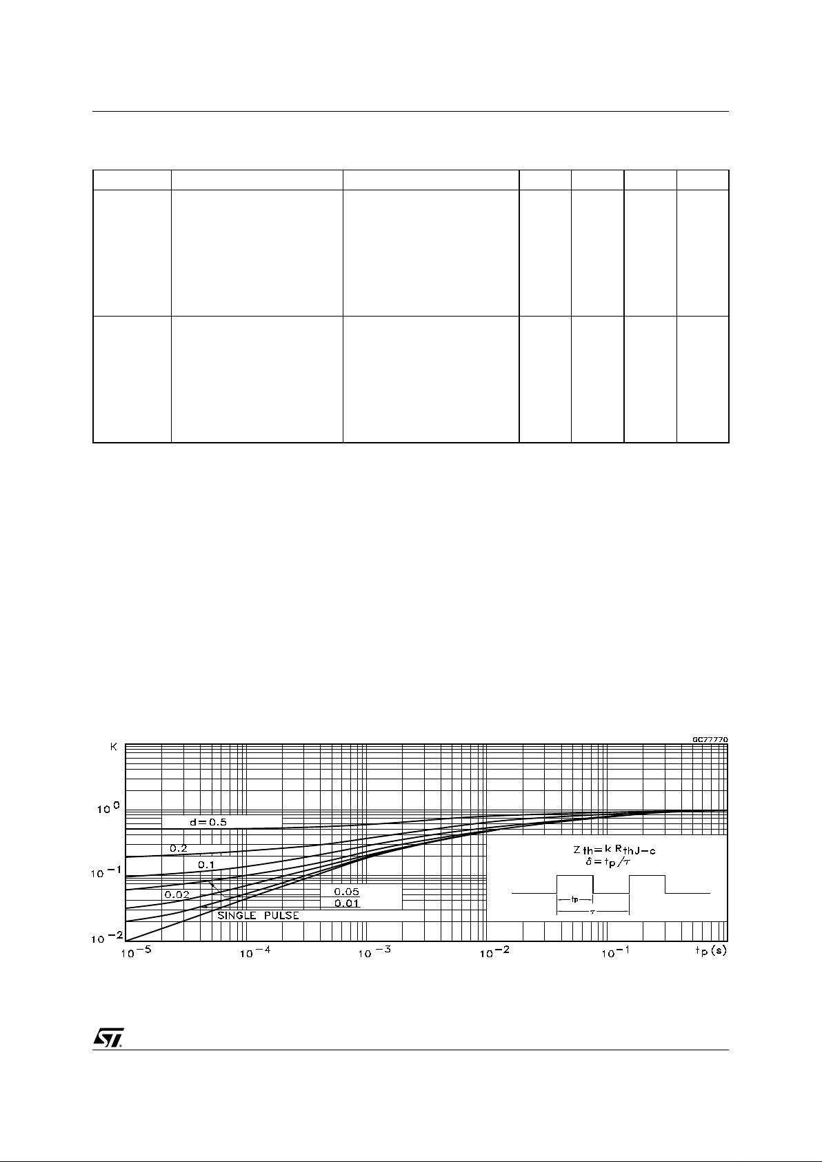
Thermal Impedance
Page 4

STGD7NB60H
4/9
Collector-Emitter On Voltage vs Collettor Current
Transconductance
Transfer Characteristics
Output Characteristics
Collector-Emitter On Voltage vs Temperature
Gate Threshold vs Temperature
Page 5

5/9
STGD7NB60H
Total Switching Losses vs Tempera ture
Total Switching Losses vs Gate ResistanceGate Charge vs Gate-Emitter Voltage
Capacitance Variations
Normalized Breakdown Volta ge vs Temperature
Total Switching Losses vs Collector Current
Page 6

STGD7NB60H
6/9
Switching Off Safe Operating Area
Page 7

7/9
STGD7NB60H
Fig. 2: Test Circuit For Inductive Load SwitchingFig. 1: Gate Charge test Circuit
Page 8

STGD7NB60H
8/9
DIM.
mm inch
MIN. TYP. MAX. MIN. TYP. MAX.
A 2.20 2.40 0.087 0.094
A1 0.90 1.10 0.035 0.043
A2 0.03 0.23 0.001 0.009
B 0.64 0.90 0.025 0.035
B2 5.20 5.40 0.204 0.213
C 0.45 0.60 0.018 0.024
C2 0.48 0.60 0.019 0.024
D 6.00 6.20 0.236 0.244
E 6.40 6.60 0.252 0.260
G 4.40 4.60 0.173 0.181
H 9.35 10.10 0.368 0.398
L2 0.8 0.031
L4 0.60 1.00 0.024 0.039
V2 0
o
8
o
0
o
0
o
P032P_B
TO-252 (DPAK) MECHANICAL DATA
Page 9

9/9
STGD7NB60H
Information furnished is believed to be accurate and reliable. However, STMicroelectronics assumes no responsibility for the consequences
of use of such informa tion n or for an y infring ement of patent s or other rig hts of third part ies which may resu lt from its use . No l i cen se i s
granted by implication or otherwise under any patent or patent rights of STMicro electronics. Specification mentioned in this publication are
subject to change without notice. This publication supersedes and replaces all information previously supplied. STMicroelectronics products
are not authorized for use as critical compo nents in life support devices or systems without express written approval of STMicroelectronics.
The ST logo is a trademark of STMicroelectronics
© 2000 STMicroelectronics – Printed in Italy – All Rights Reserved
STMicroelectronics GROUP OF COMPANIES
Australia - Brazil - China - Finland - France - Germany - Hong Kong - India - Italy - Japan - Malaysia - Malta - Morocco -
Singapore - Spain - Sweden - Switzerland - United Kingdom - U.S.A.
http://www.st.com
 Loading...