

Datasheet SP690RCN, SP690RCP, SP690REN, SP690REP, SP690SCN Datasheet (Sipex Corporation)
...
®
SP690T/S/R, SP802T/S/R,
SP804T/S/R, and SP805T/S/R
3.0V/3.3V Low P o wer Micropr ocessor
Supervisory with Battery Switch-Over
■ RESET and RESET Outputs
■ Reset asserted down to V
■ Reset Time Delay - 200ms
■ Watchdog Timer - 1.6 sec timeout
■ 40µA Maximum VCC Supply Current
■ 1µA Maximum Battery Supply Current
■ Power Switching
50mA Output in VCC Mode (1.5Ω)
10mA Output in Battery Mode (15Ω)
■ Battery Can Exceed VCC in Normal Operation
■ Precision Voltage Monitor for Power-Fail
or Low-Battery Warning
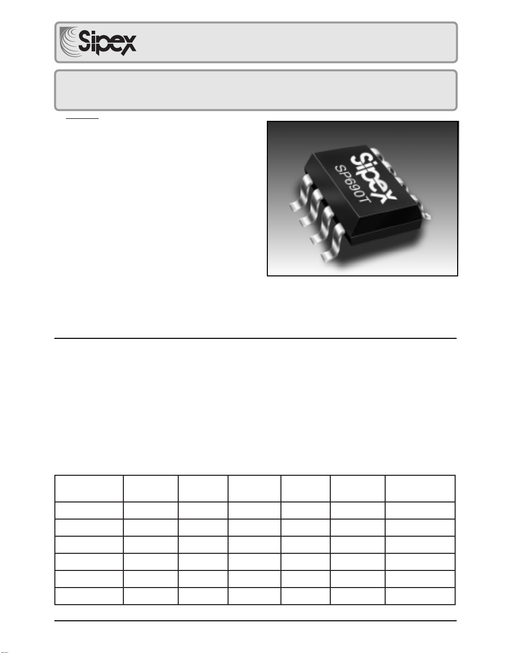
■ Available in 8 pin SO and DIP packages
■ Pin Compatible Upgrades to
MAX690T/S/R, MAX802T/S/R,
MAX804T/S/R, MAX805T/S/R
CC
= 1V
DESCRIPTION
The SP690T/S/R, SP802T/S/R, SP804T/S/R and SP805T/S/R devices are a family of
microprocessor (µP) supervisory circuits that integrate a myriad of components involved in
discrete solutions to monitor power-supply and battery-control functions in µP and digital
systems. The series will significantly improve system reliability and operational efficiency
when compared to discrete solutions. The features of the SP690T/S/R, SP802T/S/R,
SP804T/S/R and SP805T/S/R devices include a watchdog timer, a µP reset and backup-
battery switchover, and power-failure warning; a complete µP monitoring and watchdog
solution. The series is ideal for 3.0V or 3.3V applications in portable electronics, computers,
controllers, and intelligent instruments and is a solid match for designs where it is critical to
monitor the power supply to the µP and it’s related digital components. Refer to Sipex's
SP690A/692A/802L/802M/805L/805M series for similar devices designed for +5V systems.
rebmuNtraP
T508/T096PSHGIH/WOLV570.3Vm57±%4±SEYSEY
T408/T208PSHGIH/WOLV570.3Vm06±%2±SEYSEY
S508/S096PSHGIH/WOLV529.2Vm57±%4±SEYSEY
S408/S208PSHGIH/WOLV529.2Vm06±%2±SEYSEY
R508/R096PSHGIH/WOLV526.2Vm57±%4±SEYSEY
R408/R208PSHGIH/WOLV526.2Vm06±%2±SEYSEY
TESER
evitcAevitcA
evitcAevitcA
evitcA
TESER
dlohserhTdlohserhT
dlohserhTdlohserhT
dlohserhT
TESER
ycaruccAycaruccA
ycaruccAycaruccA
ycaruccA
IFP
ycaruccAycaruccA
ycaruccAycaruccA
ycaruccA
godhctaW
tupnItupnI
tupnItupnI
tupnI
yrettaB-pukcaB
hctiwShctiwS
hctiwShctiwS
hctiwS
SP690T/S/R DS/10 SP690T/S/R, 802/T/S/R, 804T/S/R, 805T/S/R Low Power Microprocessor Supervisory © Copyright 2000 Sipex Corporation
1
ABSOLUTE MAXIMUM RATINGS
These are stress ratings only and functional operation of the device at
these ratings or any other above those indicated in the operation
sections of the specifications below is not implied. Exposure to absolute
maximum rating conditions for extended periods of time may affect
reliability and cause permanent damage to the device.
VCC..................................................................................-0.3V to 6.0V
V
................................................................................-0.3V to 6.0V
BATT
All Other Inputs (NOTE 1).................................-0.3V to the higher of VCC or V
Continuous Input Current:
VCC..................................................................................100mA
V
..................................................................................20mA
BATT
GND..................................................................................20mA
WDI, PFI...........................................................................20mA
Continuous Output Current:
RESET, RESET, PFO.........................................................20mA
V
......................................................................................100mA
OUT
Power Dissipation per Package:
8pin NSOIC (derate 6.14mW/°C above +70°C)..............500mW
8pin PDIP (derate 11.8mW/°C above +70°C)..............1,000mW
Storage Temperature........................................-65°C to +160°C
Lead Temperature(soldering,10sec).............................................+300°C
ESD Rating........................................................4KV Human Body Model
BATT
SPECIFICATIONS
VCC = 3.17V to 5.50V for the SP690T/SP80_T, VCC = 3.02V to 5.50V for the SP690S/SP80_S, VCC = 2.72V to 5.50V for the SP690R/SP80_R, V
TA = T
to T
unless otherwise noted. Typical values taken at T
MIN
MAX
SRETEMARAP.NIM.PYT.XAMSTINUSNOITIDNOC
VCCVro
V
CC
V
CC
,ETON1
YRETTAB
I,tnerruCylppuS
edoMpukcaB
V
YRETTAB
,edoMynAETON2
V
YRETTAB
V
YRETTAB
V,egatloVtuptuO
TUO
V
TUO
VCCgnillaf
V
CC
7ETON,gnisir
,egnaRegatloVgnitarepO0.15.5stloV
YLPPUS
yrettaBnitnerruCylppuS
nitnerruCylppuS
ETON,tnerruCegakaeL3
ETON,tnerruCegakaeL41.0-
V
CC
V
CC
V
CC
edoMpukcaB-yrettaBniV
,dlohserhThctiwSyrettaB
YRETTAB
560.0
03.2
,dlohserhThctiwSyrettaB
= +25OC.
AMB
5204
0204
4.01
100.05.0
30.0-
V
3.0-
5100.0-
V
20.0-V
V
V
5700.0-
CC
V
570.0-
CC
3000.0-
CC
YRETTAB
YRETTAB
51.0-
YRETTAB
520.0
04.205.2
20.0
5400.0-
810.0-
µA
V
µA
µA
CC
Ignidulcxe
TUO
V,V0.2=
Ignidulcxe
TUO
Ignidulcxe
TUO
YRETTAB
µA
V>V3.3
µA
V>
CC
Am5=I
V
I
I
I
V
I
I
V
V
V
Am05=
TUO
052=µV,A
TUO
TUO
TUO
TUO
CC
V,Aµ052=
V,Am1=
BV,Am01=
V-
V,
YRETTAB
CC
V>
YRETTAB
CC
WS
V
,V3.2=
YRETTAB
V5.2>
YRETTAB
YRETTAB
YRETTA
V>
CC
6ETON,
VtaseulavdlohserhT
CC
= 3.60V, and
BATT
V2.0+
V3.2=
V3.2=
V3.3=
5ETON,V57.1>
teseRehtotlacitnedieraseulaV
gnisir
SP690T/S/R DS/10 SP690T/S/R, 802/T/S/R, 804T/S/R, 805T/S/R Low Power Microprocessor Supervisory © Copyright 2000 Sipex Corporation
2
SPECIFICATIONS (continued)
VCC = 3.17V to 5.50V for the SP690T/SP80_T, VCC = 3.02V to 5.50V for the SP690S/SP80_S, VCC = 2.72V to 5.50V for the SP690R/SP80_R, V
TA = T
to T
unless otherwise noted. Typical values taken at T
MIN
MAX
SRETEMARAP.NIM.PYT.XAMSTINUSNOITIDNOC
V,dlohserhTteseR
TSR
8ETON
teseRt,doirePtuoemiT
PW
V,egatloVtuptuOTESER
LO
11ETON
TESERdnaOFP
t,tuoemiTgodhctaW
DW
htdiWesluPIDW00204sn
dlohserhTtupnIIDW
V
HI
V
LI
tnerruCtupnIIDW1-10.01
dlohserhTtupnIIFP002.1
tnerruCtupnIIFP52-10.052An
V,siseretsyHIFP
HFP
V
V,egatloVtuptuOOFP,TESER
HO
CC
V,egatloVtuptuOOFP,TESER
LO
V,egatloVtuptuOOFP,TESER
LO
,tnerruCegakaeLtuptuOTESER
I,tnerruCDNGottrohStuptuO
,
SO
= +25OC.
AMB
00.3
00.3
58.2
58.2
55.2
55.2
00.3
00.3
88.2
88.2
95.2
95.2
570.3
580.3
529.2
539.2
526.2
536.2
570.3
580.3
529.2
539.2
526.2
536.2
51.3
71.3
00.3
20.3
07.2
27.2
21.3
41.3
00.3
20.3
07.2
27.2
V
V
041002082sm
3.0-VCC51.0-VI
I
60.003.0V
KNIS
V
CC
31.003.0VV
I
60.003.0V
1-1-
081005
µA
µA
21.106.142.2sV
Vx7.0
Vx3.0
CC
CC
KNIS
V
CC
V
V
V
CC
CC
V
µA
52.1
522.1
52.1
003.1
V
572.1
Aµ03=
ECRUOS
V=
TSR
YRETTAB
V=
TSR
YRETTAB
TESER
V,V3.3=
V6.3<
V<V0
CC
0102VmV,gnisirIFP
V,T508/T096PS
CC
V,T508/T096PS
CC
V,S508/S096PS
CC
V,S508/S096PS
CC
V,R508/R096PS
CC
V,R508/R096PS
CC
V,T408/T208PS
CC
V,T408/T208PS
CC
V,S408/S208PS
CC
V,S408/S208PS
CC
V,R408/R208PS
CC
V,R408/R208PS
CC
muminim
V,V0=
CC
mumixam
V,V0=
V=
CC
VroV0=
CC
V0=
HO
V5.5<
<V,V6.3
V,_508/_096PS
CC
<V,V6.3
V,_408/_208PS
CC
<V6.3
CC
= 3.60V, and
BATT
gnillaf
gnisir
gnillaf
gnisir
gnillaf
gnisir
gnillaf
gnisir
gnillaf
gnisir
gnillaf
gnisir
erehw_208/_096PS,Am2.1=
I,V0.1=
KNIS
Aµ04=
erehw_508/_408PS,Am2.1=
TSR
,muminim
gnillaf
IFP
gnillaf
IFP
SP690T/S/R DS/10 SP690T/S/R, 802/T/S/R, 804T/S/R, 805T/S/R Low Power Microprocessor Supervisory © Copyright 2000 Sipex Corporation
3

SPECIFICATIONS (continued)
VCC = 3.17V to 5.50V for the SP690T/SP80_T, VCC = 3.02V to 5.50V for the SP690S/SP80_S, VCC = 2.72V to 5.50V for the SP690R/SP80_R, V
TA = T
to T
unless otherwise noted. Typical values taken at T
MIN
MAX
AMB
= +25OC.
= 3.60V, and
BATT
NOTE 1: The following are tested at V
= 3.6V and VCC = 5.5V: VCC supply current, watchdog
BATT
functionality, logic input leakage, PFI functionality, and the RESET and RESET states. The state of
RESET or RESET and PFO is tested at VCC = VCC(min).
NOTE 2: Tested V
= 3.6V, VCC = 3.5V and 0V.
BATT
NOTE 3: Leakage current into the battery is tested under the following worst-case conditions: V
= 5.5V, V
= 1.8V and at VCC = 1.5V, V
BATT
BATT
= 1.0V.
NOTE 4: "-" equals the battery-charging current, "+" equals the battery-discharging current.
NOTE 5: When VSW > VCC > V
VCC-to-V
NOTE 6: When V
comparator has a small 25mV typical hysteresis to prevent oscillation.
BATT
> VCC > VSW, V
BATT
BATT
, V
remains connected to VCC until VCC drops below V
OUT
remains connected to VCC until VCC drops below the battery
OUT
BATT
. The
switch threshold, VSW.
NOTE 7: V
V
. Switchover back to VCC occurs at the exact voltage that causes RESET to go HIGH (on the
BATT
switches from V
OUT
to VCC when VCC rises above the reset threshold, independent of
BATT
SP804_ and SP805_ RESET goes LOW). Switchover occurs 200ms prior to reset.
NOTE 8: The reset threshold tolerance is wider for VCC rising than for VCC falling to accommodate the
10mV typical hysteresis, which prevents internal oscillation.
NOTE 9: SP690_ and SP802_ devices only.
NOTE 10: SP804_ and SP805_ devices only.
NOTE 11: The leakage current into or out of the RESET pin is tested with RESET asserted (RESET
output high impedance).
CC
SP690T/S/R DS/10 SP690T/S/R, 802/T/S/R, 804T/S/R, 805T/S/R Low Power Microprocessor Supervisory © Copyright 2000 Sipex Corporation
4
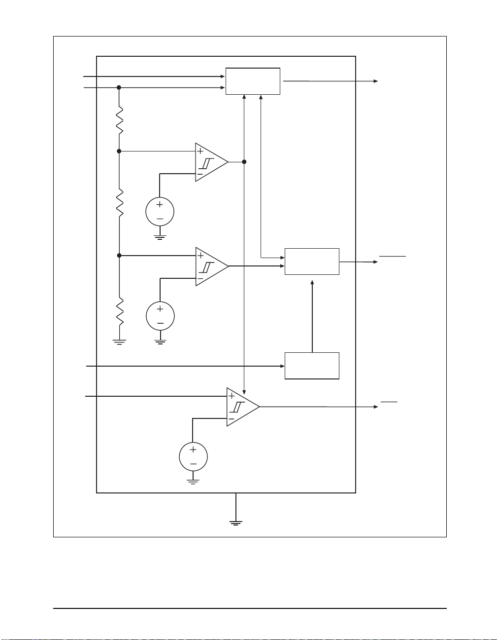
INTERNAL BLOCK DIAGRAM
V
BATT
V
CC
8
2
BATTERY
SWITCHOVER
CIRCUIT
V
OUT
1
SP690T/S/R
SP802T/S/R
SP804T/S/R
BATTERY
SWITCHOVER
COMPARATOR
1.25V
RESET
COMPARATOR
1.25V
SP805T/S/R
RESET
GENERATOR
RESET / RESET*
7
WDI
PFI
6
4
WATCHDOG
TIMER
PFO
5
POWER-FAIL
COMPARATOR
1.25V
3
GND
SP690T/S/R DS/10 SP690T/S/R, 802/T/S/R, 804T/S/R, 805T/S/R Low Power Microprocessor Supervisory © Copyright 2000 Sipex Corporation
*SP804T/S/R and SP805T/S/R only
5
PINOUT
V
V
GND
OUT
CC
1
SP690T/S/R
2
SP802T/S/R
SP804T/S/R
3
SP805T/S/R
PFI
PIN ASSIGNMENTS
Pin 1 —V
CMOS RAM. When VCC is above the
reset threshold, V
through a P-channel MOSFET switch.
When VCC falls below the VSW and
V
Connect to VCC if no battery is used.
Pin 2 — VCC — +5V Supply Input
Pin 3 — GND — Ground reference for all
signals
Pin 4 — PFI — Power-Fail Comparator Input.
When PFI is less than 1.25V or when V
falls below the VSW, PFO goes LOW,
otherwise PFO remains HIGH. Connect
to GND if unused.
Pin 5 — PFO — Power-Fail Comparator
Output. Leave open if unused.
— Output Supply Voltage for
OUT
connects to V
OUT
BATTERY
, V
BATTERY
connects to V
4
CC
OUT
CC
8
V
BATTERY
7
RESET / RESET*
6
WDI
PFO
5
*SP804T/S/R and SP805T/S/R only
Pin 7 for SP690_/802_ only — Active-LOW
Reset Output. — Whenever RESET is
triggered by a watchdog timeout, it goes
LOW for 200ms. It stays LOW whenever
VCC is below the reset threshold and re-
.
mains LOW for 200ms after VCC rises
above the reset threshold or when the
watchdog triggers a reset.
Pin 7 for SP804_/805_ only — Active-HIGH
Open-Drain Reset Output. — The
inverse operation of RESET.
Pin 8 — V
BATTERY
When VCC falls below VSW and V
V
switchesfrom VCC to V
OUT
When VCC rises above the reset threshold,
V
reconnects to VCC. V
OUT
exceed VCC. Connect to VCC if no battery
— Backup-Battery Input.
is used.
BATTERY
BATTERY
BATTERY
,
.
may
Pin 6 — WDI — Watchdog Input. If WDI
remains HIGH or LOW for 1.6 seconds,
the internal watchdog timer triggers a
reset. The internal watchdog timer clears
when reset is asserted or WDI sees a
rising or falling edge. The watchdog
function cannot be disabled.
SP690T/S/R DS/10 SP690T/S/R, 802/T/S/R, 804T/S/R, 805T/S/R Low Power Microprocessor Supervisory © Copyright 2000 Sipex Corporation
6

TYPICAL CHARACTERISTICS (T
= 25oC, unless otherwise noted)
AMB
40
35
30
Supply Current (µA)
25
20
-60 -40 -20 0 20 40 60 80 100 120 140
Temperature (
o
C)
Figure 1. VCC Supply Current vs. Temperature (Normal
Mode)
1.262
1.26
1.258
1.256
1.254
PFI Threshold (Volts)
1.252
1.25
1.248
-60 -40 -20 0 20 40 60 80 100 120 140
Temperature (
o
C)
10000
1000
100
10
Current (nA)
Battery Supply
1
0.1
-60 -35 -10 15 40 65 90 115 140
Temperature (
o
C)
Figure 2. Battery Supply Current vs. Temperature
30
25
20
15
On-Resistance (Ω)
OUT
10
to V
5
BATTERY
V
0
-60 -40 -20 0 20 40 60 80 100 120 140
Temperature (
o
C)
Figure 3. PFI Threshold vs. Temperature
3.5
3
2.5
2
1.5
On Resistance (Ω)
1
0.5
0
-60 -40 -20 0 20 40 60 80 100 120 140
Temperature (
Figure 5. VCC to V
On-Resistance vs. Temperature Figure 6. Reset Threshold vs. Temperature
OUT
o
C)
Figure 4. V
3.15
3.13
3.11
3.09
Reset Threshold (Volts)
3.07
3.05
to V
BATTERY
-60 -35 -10 15 40 65 90 115 140
ON-Resistance vs. Temperature
OUT
o
Temperature (
C)
SP690T/S/R DS/10 SP690T/S/R, 802/T/S/R, 804T/S/R, 805T/S/R Low Power Microprocessor Supervisory © Copyright 2000 Sipex Corporation
7

14000
12000
10000
185
8000
6000
4000
RESET Output Resistance (Ω)
2000
0
-60 -35 -10 15 40 65 90 115 140
Temperature (
o
C)
Figure 7. Reset Output Resistance vs. Temperature
1E-06
decade
/div
1E-14
.0000
V3 .5000/div (V)
5.000
180
Reset Timeout (mS)
175
-60 -40 -20 0 20 40 60 80 100 120 140
Temperature (
o
C)
Figure 8. Reset Timeout vs. Temperature
30
26
22
18
Propagation Delay (µs)
14
10
-60 -40 -20 0 20 40 60 80 100 120 140
Temperature (
o
C)
Figure 9. Battery Current vs. VCC Voltage
Figure 10. Reset-Comparator Propagation Delay vs.
Temperature
1000
VCC = 4.5V
V
= 0V
]
OUT
- V
100
CC
10
Voltage Drop (mV) [ V
Figure 11. VCC to V
BATTERY
1
1
OUT
10
I
(mA)
OUT
100
Vs. Output Current Figure 12. V
SP690T/S/R DS/10 SP690T/S/R, 802/T/S/R, 804T/S/R, 805T/S/R Low Power Microprocessor Supervisory © Copyright 2000 Sipex Corporation
1000
VCC = 0V
V
]
OUT
- V
BATTERY
100
BATTERY
10
Voltage Drop (mV) [ V
1
1
to V
BATTERY
= 4.5V
(mA)
I
OUT
Vs. Output Current
OUT
10
8

V
CC
V
T
A
V
RESET
CC
V
CC
2V
div
T
0V
BATTERY
= +25 C
RESET
= 0V
2KΩ
RESET
0V
1
1 sec / div
Figure 13A. SP690A RESET Output Voltage vs.
Supply Voltage
V
1V
div
0V
RESET
0V
CC
1
1 sec /div
Figure 14A. SP805L RESET Output Voltage vs.
Supply Voltage
1V / div
3.1V
2V
3.1V
[ T ]
V
CC
RESET
1
T
330pF
GND
Figure 13B. Circuit for the SP690A/802L RESET
Output Voltage vs. Supply Voltage
V
CC
V
CC
V
CC
10KΩ
RESET
V
BATTERY
330pF
GND
Figure 14B. Circuit for the SP805 RESET Output
Voltage vs. Supply Voltage
V
CC
T
= +25 C
A
V
CC
10KΩ
RESET
0
30pF
10µS / div
GND
Figure 15A. SP690A RESET Response Time
SP690T/S/R DS/10 SP690T/S/R, 802/T/S/R, 804T/S/R, 805T/S/R Low Power Microprocessor Supervisory © Copyright 2000 Sipex Corporation
Figure 15B. Circuit for the SP690A/802L RESET
Response Time
9

1V / div
V
[ T ]
V
3.1V
2V
CC
1
CC
V
CC
V
CC
10KΩ
RESET
T
0V
10 µs / div
Figure 16A. SP805L RESET Response Time
1.3V
5V
0V
PFO
PFI
1.2V
500ns / div
RESET
330pF
GND
Figure 16B. Circuit for the SP805 RESET Response
Time
+5V
V
= +5V
= 5V
V
CC
V
BATTERY
= 0
CC
T
= +25 C
A
1KΩ
PFI
PFO
+1.25V
30pF
Figure 17A. Power-Fail Comparator Response Time (fall)
Figure 17B. Circuit for the Power-Fail Comparator
Response Time (fall)
1
1.2V
1
T
2
1.3V
PFI
= 5
V
CC
V
= 0
BATTERY
PFO
500ns / div
Figure 18A. Power-Fail Comparator Response Time (rise)
Figure 18B. Circuit for the Power-Fail Comparator
PFI
+1.25V
+5V
V
T
PFO
= +5V
CC
= +25 C
A
30pF
1KΩ
Response Time (rise)
SP690T/S/R DS/10 SP690T/S/R, 802/T/S/R, 804T/S/R, 805T/S/R Low Power Microprocessor Supervisory © Copyright 2000 Sipex Corporation
10

V
CC
3.0V or 3.3V
0V
3.0V or 3.3V
V
RST
V
SW
V
OUT
3.0V or 3.3V
RESET
3.0V or 3.3V
RESET*
3.0V or 3.3V
PFO
*SP804T/S/R and SP805T/S/R only; Reset externally pulled up to V
Figure 19. Timing Diagram
0V
0V
0V
0V
V
V
SW
BATTERY
=3.6V
t
WP
V
BATTERY
I
OUT
=0mA
=PFI=3.6V
CC
.
SP690T/S/R DS/10 SP690T/S/R, 802/T/S/R, 804T/S/R, 805T/S/R Low Power Microprocessor Supervisory © Copyright 2000 Sipex Corporation
11

FEATURES
THEORY OF OPERATION
The SP690T/S/R, SP802T/S/R, SP804T/S/R
and SP805T/S/R devices provide four key
functions:
1. A battery backup switch for CMOS RAM,
CMOS microprocessors, or other logic.
2. A reset output during power-up, power-down
and brownout conditions.
3. A reset pulse if the optional watchdog timer
has not been toggled within a specified time.
4. A 1.25V threshold detector for power-fail
warning, low battery detection, or to monitor a
power supply other than 3.3V or 3.0V.
The SP690T/S/R, SP802T/S/R, SP804T/S/R
and SP805T/S/R devices differ in their reset-
voltage threshold levels and are ideally suited
for applications in automotive systems, intelligent
instruments, and battery-powered computers and
controllers. The series is a solid match for
designs where it is critical to monitor the
power supply to the µP and it’s related digital
components.
Regulated +3.3V or +3.0V
V
SP690T/S/R
SP802T/S/R
SP804T/S/R
SP805T/S/R
GND
Unregulated
DC
CC
PFI
V
BATTERY
Lithium
3.6V
Battery
R
1
R
2
V
µP
BUS
CMOS
RAM
GND
CC
RESET
NMI
I/O LINE
GND
V
CC
0.1µF
pin 7*
PFO
WDI
V
0.1µF
OUT
The SP690T/S/R, SP802T/S/R, SP804T/S/R
and SP805T/S/R devices are microprocessor
(µP) supervisory circuits that monitor the power
supplied to digital circuits such as microprocessors, microcontrollers, or memory. The series is
an ideal solution for portable, battery-powered
equipment that requires power supply monitoring.
Implementing this series will reduce the
number of components and overall complexity.
The watchdog functions of this product family
will continuously oversee the operational status
of a system.
These µP supervisory circuits are not shortcircuit protected. Shorting V
excluding power-up transients such as charging
to ground -
OUT
a decoupling capacitor - may potentially damage
these devices. Decouple both VCC and V
pins to ground by placing 0.1µF capacitors as
BATTERY
close to the device as possible. The operational
features and benefits of the SP690T/S/R,
SP802T/S/R, SP804T/S/R and SP805T/S/R
devices are described in more detail below.
Reset Output
The microprocessor's (µP's) reset input starts
the µP in a known state. When the µP is in an
unknown state, it should be held in reset. The
SP690T/S/R, SP802T/S/R, SP804T/S/R and
SP805T/S/R devices assert reset during
power-up and prevent code execution errors
during power-down or brownout conditions.
RESET is guaranteed to be a logic LOW for 0V
< VCC < V
than 1V. Without a backup battery, RESET is
guaranteed valid for VCC > 1V. Once V
exceeds the reset threshold, an internal timer
, provided that V
RST
BATTERY
is greater
CC
keeps RESET low for the reset timeout period.
After this period, RESET goes HIGH, as seen in
Figure 19.
RESET for the SP690T/S/R and the SP802T/S/R
*
RESET for the SP804T/S/R and the SP805T/S/R
Figure 20. Typical Operating Circuit
If a brownout condition occurs and VCC dips
below the reset threshold, RESET goes LOW.
Each time RESET is triggered, it stays low for
the reset timeout period. Any time VCC goes
below the reset threshold, the internal timer
restarts.
SP690T/S/R DS/10 SP690T/S/R, 802/T/S/R, 804T/S/R, 805T/S/R Low Power Microprocessor Supervisory © Copyright 2000 Sipex Corporation
12

The watchdog timer can also initiate a reset.
Refer to the Watchdog Input section.
The SP804T/S/R and SP805T/S/R active-HIGH
RESET output is open drain and the inverse
of the SP690T/S/R and SP802T/S/R RESET
outputs.
RESET is also triggered by a watchdog timeout.
If WDI remains either high or low for a period
that exceeds the watchdog timeout period (1.6
sec), RESET pulses low for 200mS. As long as
RESET is asserted, the watchdog timer remains
cleared. When RESET comes high, the watchdog resumes timing and must be serviced within
1.6sec. If WDI is tied high or low, a RESET
pulse is triggered every 1.8sec (tWD plus tRS).
Reset Threshold
The SP690T and SP805T devices are designed
for 3.3V systems with a ±5% power-supply
tolerance and a 10% system tolerance. Except
for watchdog faults, reset will not assert as long
as the power supply remains above 3.15V (3.3V
- 5%). Reset is guaranteed to assert before the
power supply falls below 3.0V.
The SP690S and SP805S devices are designed
for 3.3V ±10% power supplies. Except for
watchdog faults, they are guaranteed not to
assert reset as long as the supply remains above
3.0V (3.3V - 10%). Reset is guaranteed to
assert before the power supply fails below 2.85V
(VCC - 14%).
Watchdog Input
The watchdog circuit monitors the µP's activity.
If the µP does not toggle the watchdog input
(WDI) within 1.6sec, a reset pulse is triggered.
The internal 1.6sec timer is cleared by either a
reset pulse or by a transition (LOW-to-HIGH or
HIGH-to-LOW) at WDI. If WDI is tied HIGH
or LOW, a RESET pulse is triggered every
1.8sec (tWD plus tRS).
As long as reset is asserted, the timer remains
cleared and does not count. As soon as reset is
de-asserted, the timer starts counting. Unlike
the 5V SP690A series, the watchdog function
cannot be disabled.
Power-Fail Comparator
The power-fail comparator can be used as an
under-voltage detector to signal the failing of a
power supply (it is completely separate from the
rest of the circuitry and does not need to be
dedicated to this function). The PFI input is
compared to an internal 1.25V. If PFI is less than
V
, PFO goes low.
PFT
The power-fail comparator turns off and PFO
goes LOW when VCC falls below VSW on
power-down. The power-fail comparator turns
on as VCC crosses VSW on power-up. If the
comparator is not used, connect PFI to ground
and leave PFO unconnected.
Backup-Battery Switchover
The SP690R and SP805R devices are optimized
for monitoring 3.0V ±10% power supplies. Reset
will not occur until VCC falls below 2.7V (3.0V
- 10%), but is guaranteed to occur before the
supply falls below 2.55V (3.0V - 15%).
The SP802T/S/R and SP804T/S/R devices are
respectively similar to the SP690T/S/R and
SP805T/S/R devices with tightened reset
and power-fail threshold tolerances.
SP690T/S/R DS/10 SP690T/S/R, 802/T/S/R, 804T/S/R, 805T/S/R Low Power Microprocessor Supervisory © Copyright 2000 Sipex Corporation
In the event of a brownout or power failure, it
may be necessary to preserve the contents of
RAM. With a backup battery installed at
V
BATTERY
RAM to backup power when VCC fails.
, the devices automatically switch
This family of µP supervisors (designed for
3.3V and 3V systems) doesn't always connect
V
BATTERY
than VCC. V
a 15Ω switch) when VCC is below VSW and
V
BATTERY
to V
OUT
BATTERY
when V
connects to V
is greater than VCC.
BATTERY
OUT
is greater
(through
13

V
BATTERY
3.0V or 3.3V
V
CC
V
OUT
CONNECT TO
1N4148
STATIC RAM
A) B)
1N4148
+5V
V
BATTERY
3.0V or 3.3V
V
CC
V
OUT
CONNECT TO
STATIC RAM
0.1F
Figure 21. Using a High Capacity Capacitor as a Backup Power Source
pin 7*
GND
Switchover at VSW (2.40V) ensures that batterybackup mode is entered before V
close to the 2.0V minimum required to reliably
retain data in CMOS RAM. Switchover at higher
VCC voltages would decrease backup-battery
life. When VCC recovers, switchover is deferred
until VCC rises above the reset threshold, V
to ensure a stable supply. V
VCC through a 1.5Ω PMOS power switch.
CONNECT
TO µP
OUT
is connected to
OUT
gets too
RST
0.1F
Replacing the Backup Battery
If V
BATTERY
to ground, the backup battery can be removed
while VCC remains valid without danger of
triggering RESET/RESET. As long as V
,
stays above VSW, battery-backup mode cannot
be entered.
Adding Hysteresis to the Power-Fail
Using a High Capacity Capacitor as a
Comparator
Backup Power Source
The power-fail comparator has a typical input
Figure 21 shows two ways to use a High Value
Capacitor as a backup power source. The High
Value Capacitor may be connected through a
diode to the 3V input as in Figure 21A or, if a
5V supply is also available, the High Value
hysteresis of 10mV. This is sufficient for most
applications where a power-supply line is being
monitored through an external voltage divider
(refer to the Monitoring an Additional Power
Supply section).
Capacitor may be charged up to the 5V supply
as in Figure 21B allowing a longer backup
period. Since V
is above the reset threshold, there are no
can exceed VCC while V
BATTER Y
CC
special precautions when using these µP
supervisors with a High Value Capacitor.
If additional noise margin is desired, connect a
resistor between PFO and PFI as shown in
Figure 22A. Select the ratio of R1 and R2 such
that PFI sees 1.25V when VIN falls to its trip
point (V
typically be more than 10 times the value of R1
Operation Without a Backup Power
Source
or R2. The hysteresis window extends both
above (VH) and below (VL) the original trip
point (V
These µP supervisors were designed for
battery-backed applications. If a backup power
source is not used, connect both VBATTERY
and V
switch over to any backup power source, V
does not need to be switched. A direct connec-
to VCC. Since there is no need to
OUT
OUT
tion to VCC eliminates any voltage drops across
the switch which may push V
below VCC.
OUT
pin 7*
GND
RESET for the SP690T/S/R and the SP802T/S/R
*
RESET for the SP804T/S/R and the SP805T/S/R
CONNECT
TO µP
is decoupled with a 0.1µF capacitor
). R3 adds the hysteresis and will
TRIP
).
TRIP
CC
SP690T/S/R DS/10 SP690T/S/R, 802/T/S/R, 804T/S/R, 805T/S/R Low Power Microprocessor Supervisory © Copyright 2000 Sipex Corporation
14

A.)
V
IN
R1
+
R2
*C1
TOµP
V
CC
PFI
SP690T/S/R
SP802T/S/R
R3
SP804T/S/R
SP805T/S/R
PFO
GND
*OPTIONAL
B.)
V
IN
R1
+
R2
*C1
TOµP
V
CC
PFI
SP690T/S/R
SP802T/S/R
R3
SP804T/S/R
SP805T/S/R
PFO
GND
PFO
0V
0V V
V
= V
TRIP
VH =
V
PFT
(
VL = R1
[
WHERE V
V
PFT
(
+ V
PFH
)
1 + 1 + 1
V
PFT
(
R1 R2 R3
= 1.25V
PFT
PFH
L
R1 + R2
R2
R1
(
)
= 10mV
V
TRIP
)
1 + 1 + 1
(
R1 R2 R3
V
IN
V
H
)
- V
CC
)
]
R3
Figure 22A. Adding Additional Hysteresis to the Power-Fail Comparator.
Figure 22B. Shifting the Additional Hysteresis above V
Connecting an ordinary signal diode in series
with R3, as in Figure 22B, causes the lower trip
point (VL) to coincide with the trip point without
hysteresis (V
window occurs above V
vides additional noise margin without compro-
), so the entire hysteresis
TRIP
. This method pro-
TRIP
PFT
The current through R1 and R2 should be at least
1µA to ensure that the 25nA (max over extended
temperature range) PFI input current does not
shift the trip point. R3 should be larger than
10kΩ so it does not load down the PFO pin.
Capacitor C1 adds additional noise rejection.
mising the accuracy of the power-fail threshold
when the monitored voltage is falling. It is
useful for accurately detecting when a voltage
falls past a threshold.
V
IN
R1
R2
PFI
V
CC
SP690T/S/R
SP802T/S/R
SP804T/S/R
SP805T/S/R
GND
PFO
R1
R2
V-
PFO
0V
0V V
TRIP
V
H
R1 + R2
V
= V
TRIP
PFT
)
(
R2
- (V
1 + 1 + 1
V
VL = R1
PFT + VPFH
[
(
)
(
)
R1 R2 R3
WHERE V
= 1.25V
PFT
V
= 10mV
PFH
VD = DIOD FORWARD VOLTAGE DROP
3.0V OR 3.3V
V
CC
SP690T/S/R
SP802T/S/R
PFI
SP804T/S/R
SP805T/S/R
GND
PFO
R3
CC - VD
V
IN
)
]
V
PFO
V
VH =
CC
V
V
TRIP
V
R1 + R2
= V
TRIP
PFT
)
(
R2
R1 + R2
V
V
PFT
+
PFH
(
)
(
)
R2
IN
H
V
CC
PFO
V
= R2
TRIP
VL = R2
WHERE V
V
NOTE: V
V
[
(
1 + 1
V
PFT
[
(
R1 R2
= 1.25V
PFT
PFH
IS NEGATIVE
TRIP
V
L
+ V
PFT
= 10mV
V
1 + 1
PFH
)
(
R1 R2
- V
CC
)
R3
V-
0V
TRIP
- V
CC
]
)
R1
]
Figure 23. Using the Power-Fail Comparator to Monitor an Additional Power Supply
SP690T/S/R DS/10 SP690T/S/R, 802/T/S/R, 804T/S/R, 805T/S/R Low Power Microprocessor Supervisory © Copyright 2000 Sipex Corporation
15

Buffered RESET connects to System Components
V
CC
V
CC
1nF Capacitor
V
TO GND
OUT
RESET
4.7KΩ
GND
Figure 24. Interfacing to Microprocessors with
Bidirectional RESET I/O
RESET
µP
GND
Monitoring an Additional Power Supply
These µP supervisors can monitor either positive
or negative supplies using a resistor voltage
divider to PFI. PFO can be used to generate an
interrupt to the µP, as seen in Figure 23.
Interfacing to µPs with Bidirectional
Reset Pins
Any µPs with bidirectional reset pins, such as
the Motorola 68HC11 series, can interface with
the SP690_ and the SP802_ RESET outputs.
For example, if the RESET output is driven
HIGH and the µP wants to pull it LOW,
indeterminate logic levels may result. To correct
this, connect a 4.7kΩ resistor between the
RESET output and the µP reset I/O, as in
Figure 24. Buffer the RESET output to other
system components.
Above Line
RESET
NO
RESET
Generated
Figure 25. Maximum Transient Duration without
Causing a Reset Pulse vs. Reset Comparator Overdrive
Generated
Figure 25 shows maximum transient duration
vs. reset-comparator overdrive, for which reset
pulses are not generated. The data was generated
using negative-going VCC pulses, starting at
3.3V and ending below the reset threshold by
the magnitude indicated (reset comparator
overdrive). The graph shows the maximum pulse
width a negative-going VCC transient may
typically have without causing a reset pulse to
be issued. As the amplitude of the transient
increases (i.e. goes farther below the reset
threshold), the maximum allowable pulse width
decreases. Typically, a VCC transient that goes
100mV below the reset threshold and lasts for
40µs or less will not cause a reset pulse to be
issued. A 100nF bypass capacitor mounted close
to the VCC pin provides additional transient
immunity.
Negative-Going VCC Transients
While issuing resets to the µP during power-up,
power-down, and brownout conditions, these
supervisors are relatively immune to shortduration negative-going VCC transients
(glitches). It is usually undesirable to reset the
µP when VCC experiences only small glitches.
SP690T/S/R DS/10 SP690T/S/R, 802/T/S/R, 804T/S/R, 805T/S/R Low Power Microprocessor Supervisory © Copyright 2000 Sipex Corporation
16

D1 = 0.005" min.
(0.127 min.)
D
e = 0.100 BSC
(2.540 BSC)
B1
B
ALTERNATE
END PINS
(BOTH ENDS)
PACKAGE: PLASTIC
DUAL–IN–LINE
(NARROW)
E1
E
A1 = 0.015" min.
(0.381min.)
A = 0.210" max.
(5.334 max).
A2
L
C
Ø
eA = 0.300 BSC
(7.620 BSC)
DIMENSIONS (Inches)
Minimum/Maximum
(mm)
A2
B
B1
C
D
E
E1
L
Ø
0.115/0.195
(2.921/4.953)
0.014/0.022
(0.356/0.559)
0.045/0.070
(1.143/1.778)
0.008/0.014
(0.203/0.356)
0.355/0.400
(9.017/10.160)
0.300/0.325
(7.620/8.255)
0.240/0.280
(6.096/7.112)
0.115/0.150
(2.921/3.810)
0°/ 15°
(0°/15°)
0.115/0.195
(2.921/4.953)
0.014/0.022
(0.356/0.559)
0.045/0.070
(1.143/1.778)
0.008/0.014
(0.203/0.356)
0.735/0.775
(18.669/19.685)
0.300/0.325
(7.620/8.255)
0.240/0.280
(6.096/7.112)
0.115/0.150
(2.921/3.810)
0°/ 15°
(0°/15°)
0.115/0.195
(2.921/4.953)
0.014/0.022
(0.356/0.559)
0.045/0.070
(1.143/1.778)
0.008/0.014
(0.203/0.356)
0.780/0.800
(19.812/20.320)
0.300/0.325
(7.620/8.255)
0.240/0.280
(6.096/7.112)
0.115/0.150
(2.921/3.810)
0°/ 15°
(0°/15°)
18–PIN
0.115/0.195
(2.921/4.953)
0.014/0.022
(0.356/0.559)
0.045/0.070
(1.143/1.778)
0.008/0.014
(0.203/0.356)
0.880/0.920
(22.352/23.368)
0.300/0.325
(7.620/8.255)
0.240/0.280
(6.096/7.112)
0.115/0.150
(2.921/3.810)
0°/ 15°
(0°/15°)
20–PIN
0.115/0.195
(2.921/4.953)
0.014/0.022
(0.356/0.559)
0.045/0.070
(1.143/1.778)
0.008/0.014
(0.203/0.356)
0.980/1.060
(24.892/26.924)
0.300/0.325
(7.620/8.255)
0.240/0.280
(6.096/7.112)
0.115/0.150
(2.921/3.810)
0°/ 15°
(0°/15°)
22–PIN8–PIN 14–PIN 16–PIN
0.115/0.195
(2.921/4.953)
0.014/0.022
(0.356/0.559)
0.045/0.070
(1.143/1.778)
0.008/0.014
(0.203/0.356)
1.145/1.155
(29.083/29.337)
0.300/0.325
(7.620/8.255)
0.240/0.280
(6.096/7.112)
0.115/0.150
(2.921/3.810)
0°/ 15°
(0°/15°)
SP690T/S/R DS/10 SP690T/S/R, 802/T/S/R, 804T/S/R, 805T/S/R Low Power Microprocessor Supervisory © Copyright 2000 Sipex Corporation
17

D
Be
DIMENSIONS (Inches)
Minimum/Maximum
EH
A
A1
(mm)
A
A1
B
D
E
e
H
h
L
Ø
PACKAGE: PLASTIC
SMALL OUTLINE (SOIC)
(NARROW)
h x 45°
L
8–PIN
0.053/0.069
(1.346/1.748)
0.004/0.010
(0.102/0.249
0.014/0.019
(0.35/0.49)
0.189/0.197
(4.80/5.00)
0.150/0.157
(3.802/3.988)
0.050 BSC
(1.270 BSC)
0.228/0.244
(5.801/6.198)
0.010/0.020
(0.254/0.498)
0.016/0.050
(0.406/1.270)
0°/8°
(0°/8°)
14–PIN
0.053/0.069
(1.346/1.748)
0.004/0.010
(0.102/0.249)
0.013/0.020
(0.330/0.508)
0.337/0.344
(8.552/8.748)
0.150/0.157
(3.802/3.988)
0.050 BSC
(1.270 BSC)
0.228/0.244
(5.801/6.198)
0.010/0.020
(0.254/0.498)
0.016/0.050
(0.406/1.270)
0°/8°
(0°/8°)
16–PIN
0.053/0.069
(1.346/1.748)
0.004/0.010
(0.102/0.249)
0.013/0.020
(0.330/0.508)
0.386/0.394
(9.802/10.000)
0.150/0.157
(3.802/3.988)
0.050 BSC
(1.270 BSC)
0.228/0.244
(5.801/6.198)
0.010/0.020
(0.254/0.498)
0.016/0.050
(0.406/1.270)
(0°/8°)
Ø
0°/8°
SP690T/S/R DS/10 SP690T/S/R, 802/T/S/R, 804T/S/R, 805T/S/R Low Power Microprocessor Supervisory © Copyright 2000 Sipex Corporation
18

Model Temperature Range Package Types
ORDERING INFORMATION
SP690TCN......................................................0°C to +70°C......................................................8-Pin NSOIC
SP690TCP......................................................0°C to +70°C.........................................................8-Pin PDIP
SP690TEN.....................................................-40°C to +85°C....................................................8-Pin NSOIC
SP690TEP.....................................................-40°C to +85°C.......................................................8-Pin PDIP
SP690SCN......................................................0°C to +70°C......................................................8-Pin NSOIC
SP690SCP......................................................0°C to +70°C.........................................................8-Pin PDIP
SP690SEN.....................................................-40°C to +85°C....................................................8-Pin NSOIC
SP690SEP.....................................................-40°C to +85°C.......................................................8-Pin PDIP
SP690RCN......................................................0°C to +70°C......................................................8-Pin NSOIC
SP690RCP......................................................0°C to +70°C.........................................................8-Pin PDIP
SP690REN.....................................................-40°C to +85°C....................................................8-Pin NSOIC
SP690REP.....................................................-40°C to +85°C.......................................................8-Pin PDIP
SP802TCN........................................................0°C to +70°C....................................................8-Pin NSOIC
SP802TCP........................................................0°C to +70°C.......................................................8-Pin PDIP
SP802TEN.......................................................-40°C to +85°C..................................................8-Pin NSOIC
SP802TEP.......................................................-40°C to +85°C.....................................................8-Pin PDIP
SP802SCN........................................................0°C to +70°C....................................................8-Pin NSOIC
SP802SCP........................................................0°C to +70°C.......................................................8-Pin PDIP
SP802SEN.......................................................-40°C to +85......................................................8-Pin NSOIC
SP802SEP.......................................................-40°C to +85°C.....................................................8-Pin PDIP
SP802RCN........................................................0°C to 0°C........................................................8-Pin NSOIC
SP802RCP........................................................0°C to+70°C...................................................... 8-Pin PDIP
SP802REN.......................................................-40°C to +85°C..................................................8-Pin NSOIC
SP802REP.......................................................-40°C to +85°C.....................................................8-Pin PDIP
SP804TCN.......................................................0°C to +70°C.....................................................8-Pin NSOIC
SP804TCP.......................................................0°C to +70°C........................................................8-Pin PDIP
SP804TEN......................................................-40°C to +85°C...................................................8-Pin NSOIC
SP804TEP......................................................-40°C to +85°C......................................................8-Pin PDIP
SP804SCN.......................................................0°C to +70°C.....................................................8-Pin NSOIC
SP804SCP.......................................................0°C to +70°C........................................................8-Pin PDIP
SP804SEN......................................................-40°C to +85°C...................................................8-Pin NSOIC
SP804SEP......................................................-40°C to +85°C......................................................8-Pin PDIP
SP804RCN.......................................................0°C to +70°C.....................................................8-Pin NSOIC
SP804RCP.......................................................0°C to +70°C........................................................8-Pin PDIP
SP804REN......................................................-40°C to +85°C...................................................8-Pin NSOIC
SP804REP......................................................-40°C to +85°C......................................................8-Pin PDIP
SP805TCN........................................................0°C to +70°C....................................................8-Pin NSOIC
SP805TCP........................................................0°C to +70°C.......................................................8-Pin PDIP
SP805TEN.......................................................-40°C to +8C.................................................. ..8-Pin NSOIC
SP805TEP.......................................................-40°C to +85°C.....................................................8-Pin PDIP
SP805SCN........................................................0°C to+70°C.....................................................8-Pin NSOIC
SP805SCP........................................................0°C to +70°C.......................................................8-Pin PDIP
SP805SEN.......................................................-40°C to +85°C..................................................8-Pin NSOIC
SP805SEP.......................................................-40°C to +85°C.....................................................8-Pin PDIP
SP805RCN........................................................0°C to +70°C....................................................8-Pin NSOIC
SP805RCP........................................................0°C to +70°C.......................................................8-Pin PDIP
SP805REN.......................................................-40°C to +85°C..................................................8-Pin NSOIC
SP805REP.......................................................-40°C to +85°C.....................................................8-Pin PDIP
Please consult the factory for pricing and availability on a Tape-On-Reel option.
SP690T/S/R DS/10 SP690T/S/R, 802/T/S/R, 804T/S/R, 805T/S/R Low Power Microprocessor Supervisory © Copyright 2000 Sipex Corporation
19

Corporation
SIGNAL PROCESSING EXCELLENCE
Sipex Corporation
Headquarters and
Sales Office
22 Linnell Circle
Billerica, MA 01821
TEL: (978) 667-8700
FAX: (978) 670-9001
e-mail: sales@sipex.com
Sales Office
233 South Hillview Drive
Milpitas, CA 95035
TEL: (408) 934-7500
FAX: (408) 935-7600
Sipex Corporation reserves the right to make changes to any products described herein. Sipex does not assume any liability arising out of the
application or use of any product or circuit described herein; neither does it convey any license under its patent rights nor the rights of others.
SP690T/S/R DS/10 SP690T/S/R, 802/T/S/R, 804T/S/R, 805T/S/R Low Power Microprocessor Supervisory © Copyright 2000 Sipex Corporation
20
 Loading...