

GaAlAs Laser Diode
Description
The SLD105VL is a low current consumption
GaAlAs laser diode developed for CD.
Features
• Low current consumption
• Small package (φ 5.6 mm)
Applications
• Pickup for portable CD
Structure
• GaAlAs double hetero structured laser diode
• Pin photodiode for optical power output monitor
Recommended Operating Optical Power Output
2.5 mW
SLD105VL
M-260
Absolute Maximum Ratings (Ta=25 °C)
• Optical power output PO 5mV
•Reverse voltage VR LD 2 V
PD 15 V
• Operating temperature
Topr –10 to +60 °C
• Storage temperature
Tstg –40 to +85 °C
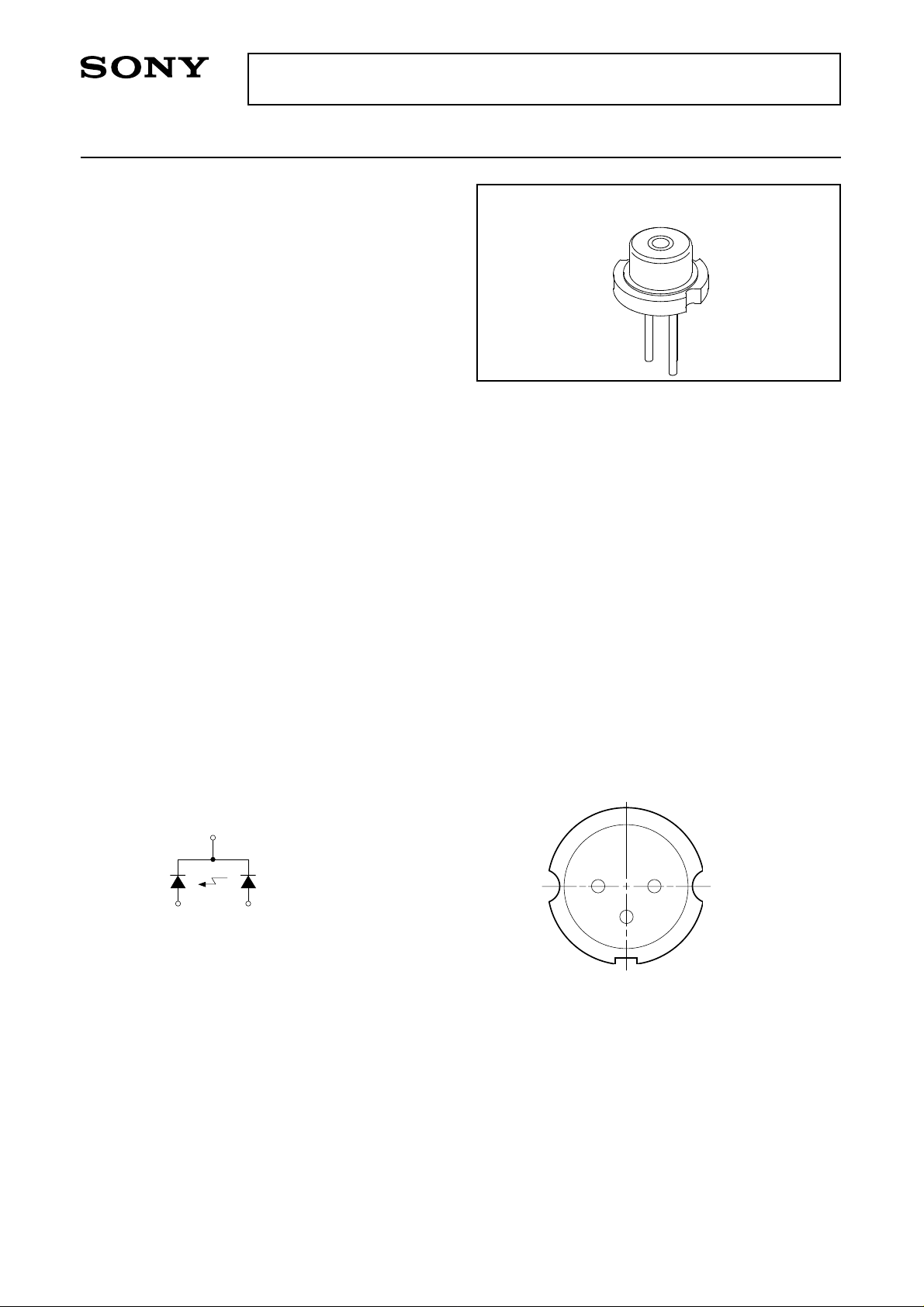
Connection Diagram Pin Configuration
COMMON
3
PD
2
Sony reserves the right to change products and specifications without prior notice. This information does not convey any license by
any implication or otherwise under any patents or other right. Application circuits shown, if any, are typical examples illustrating the
operation of the devices. Sony cannot assume responsibility for any problems arising out of the use of these circuits.
LD
1
21
3
1. LD anode
2. PD anode
3. COMMON
Bottom View
—1—
E96Y22-TE
SLD105VL
Optical and Electrical Characteristics (TC=25 °C) TC : Case temperature
Item
Threshold current
Operating current
Operating voltage
Oscillation wavelength
Monitor current
Radiation
angle
Perpendicular
Parallel
Symmetry of θ //
Positional Position
accuracy Angle
Differential efficiency
Astigmatism
S/N ratio
PD dark current
PD capacitance between pins
Symbol
Ith
Iop
Vop
λp
Im
θ ⊥
θ //
∆SR∗
∆X, ∆Y, ∆Z
∆ ⊥
ηD
AS
S/N
ID
CT
Conditions
PO=2.5 mW
PO=2.5 mW
PO=2.5 mW
PO=2.5 mW
VR=0 V
PO=2.5 mW
PO=2.5 mW
PO=2.5 mW
Z //–Z⊥
fc=720 kHz
∆f=30 kHz
PO=2.5 mW
VR=5 V
VR=5 V, f=1 kHz
Min.
1.7
760
0.08
20
8
0.2
–30
Typ.
30
35
1.9
790
0.15
39
12
0.6
–25
85
Max.
41
44
2.5
810
0.4
45
21
30
±150
±3
0.7
–20
150
30
Unit
mA
mA
V
nm
mA
degree
degree
%
µm
degree
mW/mA
µm
nA
pF
∗∆ SR
Power
S
L SR
–7° 0° 7°
θ ||
∆ S
R =
| SL – SR |
SL + SR
—2—
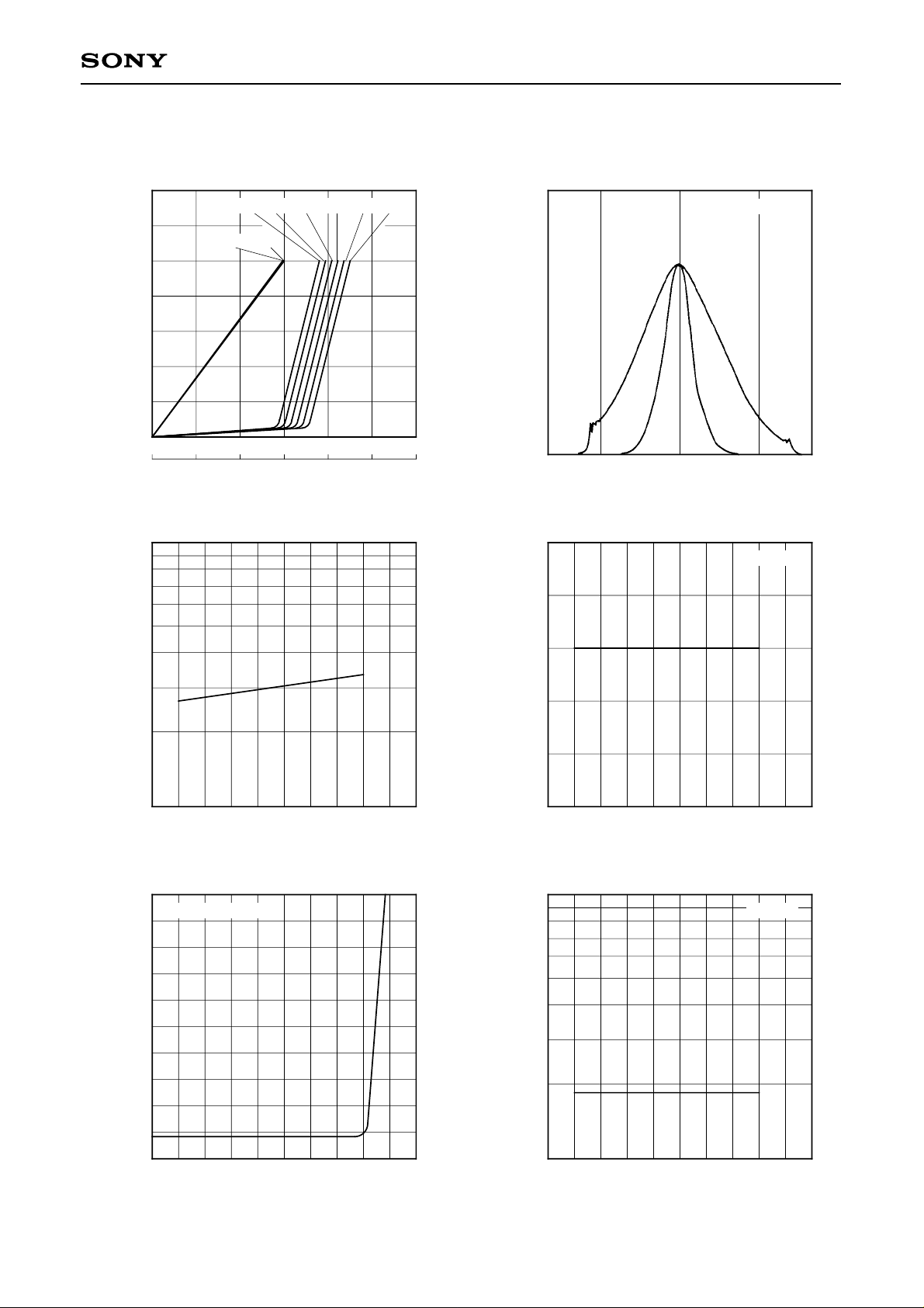
Example of Representative Characteristics
SLD105VL
Optical power output vs. Forward current characteristics
7
6
5
4
3
2
-Optical power output (mW)
O
P
1
0
010203040
0 0.1 0.2 0.3 0.4 0.5
Threshold current vs. Temperature characteristics
100
90
80
70
60
50
40
Tc=10°C 20°C 30°C 40°C 50°C 60°C
Tc=10°C 60°C
50
I
F-Forward current (mA)
IF (mA)
Imon (mA)
Far field pattern (FFP)
PO=3mW, Tc=25°C
θ⊥
Relative radiant intensity
–30 0 30
Angle (degree)
Differential efficiency vs. Temperature characteristics
1.0
0.8
0.6
θ //
PO=3mW
30
20
Ith-Threshold current (mA)
10
–20 0
Tc-Case temperature (°C)
PIN diode voltage current characteristics
0.25
PO=3mW, Tc=25°C
0
Current (mA)
20 40 60 80
0.4
0.2
ηD-Differential efficiency (mW/mA)
0
Monitor current vs. Temperature characteristics
1.000
0.800
0.600
0.500
0.400
0.300
0.200
Im-Monitor current (mA)
20 40 60 80–20 0
Tc-Case temperature (°C)
PO=3mW
–0.25
Voltage (V)
1.0–1.0 0
0.100
–20 0
20 40 60 80
Tc-Case temperature (°C)
—3—

SLD105VL
Optical power output dependence of far field pattern
(Parallel to junction)
PO=5mW
PO=4mW
PO=3mW
PO=2mW
Relative radiant intensity
–30 0 30
Angle (degree)
Temperature dependence of far field pattern
(Parallel to junction)
Optical power output dependence of far field pattern
(Perpendicular to junction)
PO=5mW
PO=4mW
PO=3mW
PO=2mW
Relative radiant intensity
–30 0 30
Angle (degree)
Temperature dependence of far field pattern
(Perpendicular to junction)
PO=3mW PO=3mW
Tc=60°C
Tc=50°C
Tc=40°C
Relative radiant intensity
–30 0 30
Angle (degree)
Tc=60°C
Tc=50°C
Tc=40°C
Tc=30°C
Tc=20°C
Relative radiant intensity
–30 0 30
Tc=30°C
Tc=20°C
Angle (degree)
—4—

Optical power output dependence of spectrum
Tc=25°C PO=5mW
O=3mW
P
SLD105VL
Relative radiant intensity
780 785 790 795 800
O=1mW
P
λ−Wavelength (nm)
—5—

O=3mW
P
SLD105VL
Temperature dependence of spectrum
Tc=50°C
Tc=25°C
Relative radiant intensity
780 785 790 795 800
Tc=0°C
λ−Wavelength (nm)
—6—

Package Outline Unit : mm
SLD105VL
M-260
Reference Slot
Reference Plane
LD Chip & Photo Diode
90°
0.25
0.5
3
0
φ5.6 – 0.05
φ4.4 MAX
φ3.7 MAX
1.0
12
123
3 – φ0.45
0.4
0.5 MIN
∗1.26
2.6 MAX
1.2 ± 0.1
6.5
SONY CODE
EIAJ CODE
JEDEC CODE
∗Optical
Distance = 1.35 ± 0.15
M-260
PCD φ2.0
PACKAGE WEIGHT
0.3g
—7—
 Loading...