

Page 1
SLB 0587
Dimmer IC for Halogen Lamps
SLB 0587
Preliminary Data CMOS IC
Features
● Phase control for resistive and inductive loads
● Sensor operation – no machanically moved
switching elements
● Operation possible from several extensions
● Capable of replacing electromechanical wall
switches in conventional light installations
● High interference immunity, even against ripple
control signals
● Programming input for selection of three different func-
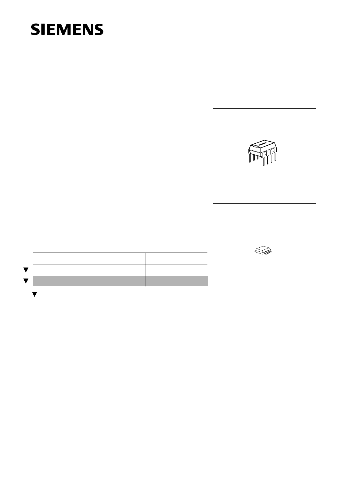
P-DIP-8
tions (mode A/B/C)
● Soft start
● Safety turn-OFF
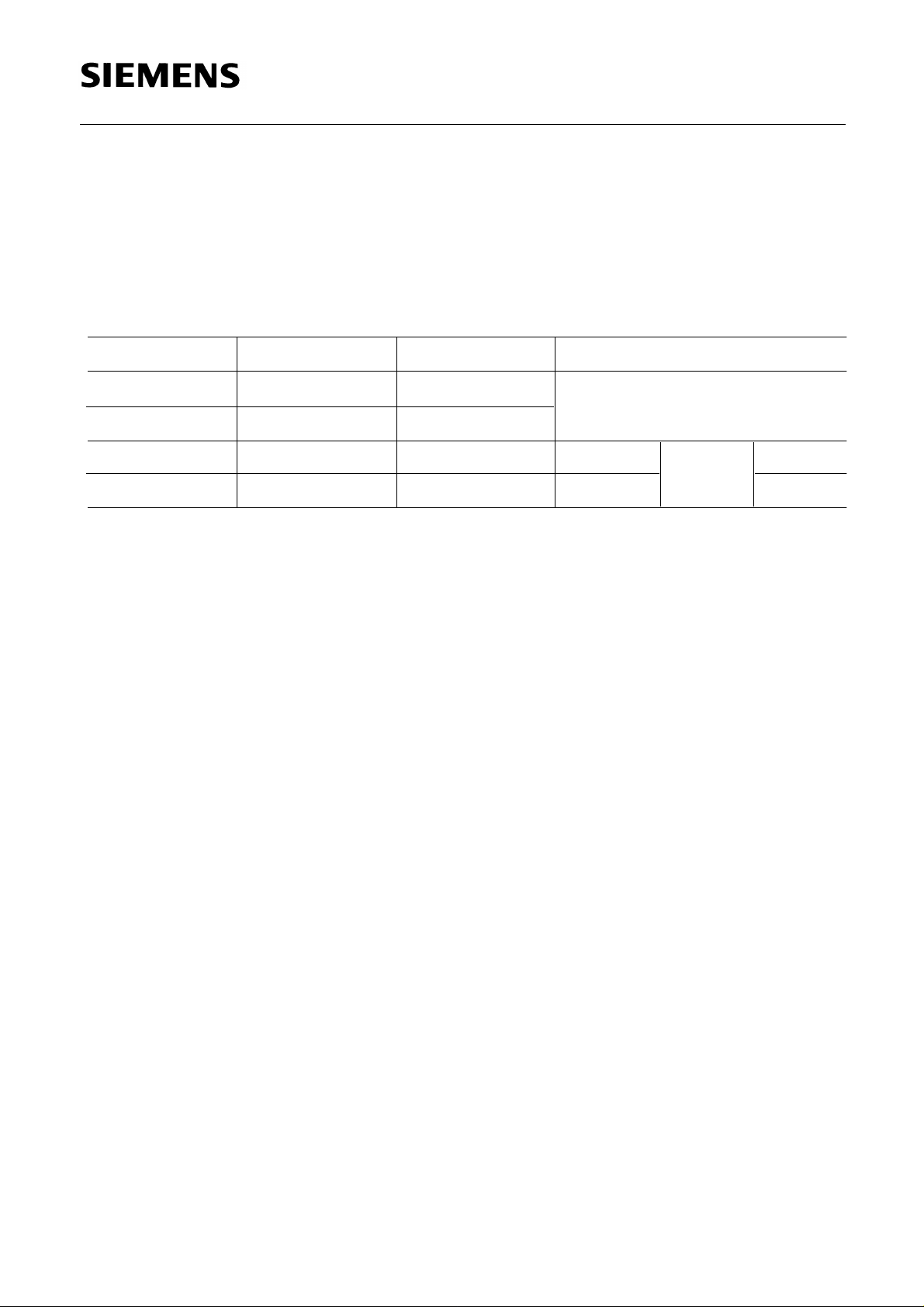
Type Ordering Code Package
SLB 0587 Q67100-A8310 P-DIP-8
SLB 0587 G Q67106-A8315 P-DSO-8-1 (SMD)
P-DSO-8-1
t New Type
For applications where the SLB 0586 A has been used, it is possible to replace the
SLB 0586 A by the SLB 0587 if the appropriate external wiring in accordance with the data
sheet is maintained.
The SLB 0587 is a CMOS IC and the advanced version of the version SLB 0586 A.
The IC permits the design of digital electronic phase controls for operation of incandes-cent
lamps, low-voltage halogen lamps with in-series connected transformers, and universal as well
as split-pole motors.
Semiconductor Group 1
09.94
Page 2
SLB 0587 SLB 0587 G
SLB 0587
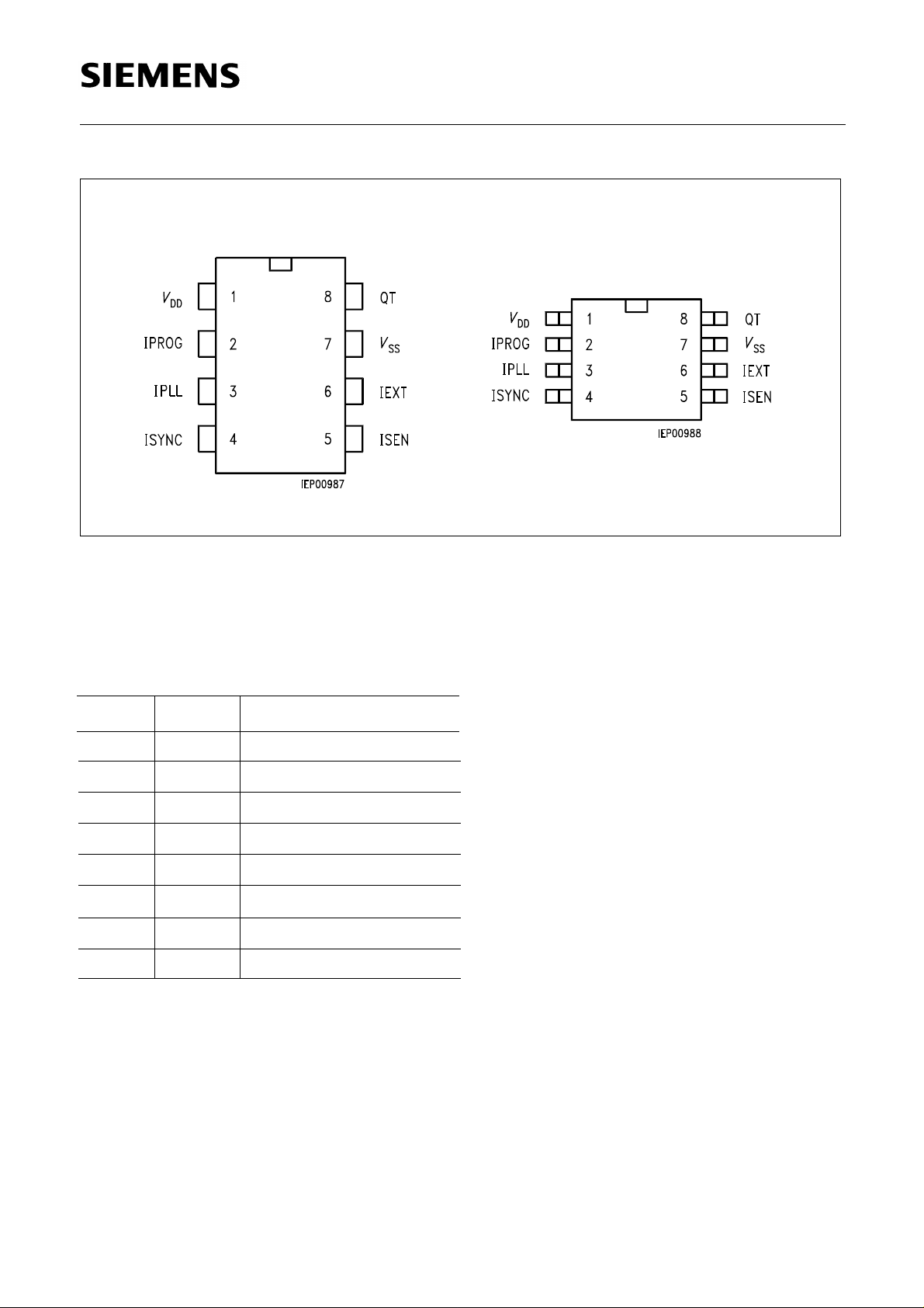
Pin Configuration (top view)
Pin Definitions and Functions
Pin Symbol Function
1
2
3
4
5
6
7
8
V DD
IPROG
IPLL
ISYNC
ISEN
IEXT
SS
V
QT
Reference point (OV)
Programming input
Integrator for PLL
Synchronizing input
Sensor input
Extension input
Supply voltage
Trigger pulse output
Semiconductor Group 2
Page 3
SLB 0587
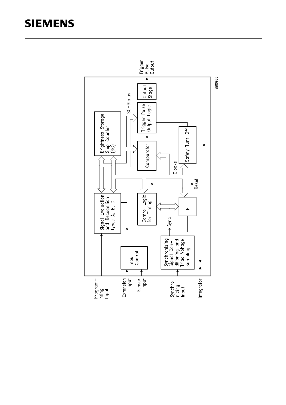
Figure 1
Block Diagram
Semiconductor Group 3
Page 4

SLB 0587
Functional Description
With the SLB 0587 it is possible to generate one defined current pulse per line half cycle.
Together with a triac and a few extra passive components, a line-powered phase-control circuit
can be designed. The phase-control angle (turn-ON time of the triac) can be set on the two
control inputs, pins 5 and 6, of the IC.
The voltage supply to the IC in a two-wire connection is ensured by limiting the angle of current
flow to approx. 152°. This makes it simple to exchange mechanical wall switches in conventional lighting installations. The IC’s internal logic is synchronized with the line by PLL. Thus a
phase control range independent of the line frequency is obtained.
Operation with Low-Voltage Halogen Lamps
In normal, resistive operation of a phase control circuit there is alternately part of the positive
and negative line-voltage half cycle applied to the load via the triac that has started to conduct
because of the trigger pulse. Operation of the circuit with a transformer and low-voltage
halogen lamp connected is largely identical to the operation of a normal filament lamp due to
the primarily resistive nature of the load. In operation with resistive and inductive portions of
load, the zero crossing of the current compared to that of the line voltage line is delayed.
In operation with heavily inductive loads (eg an idling transformer after lamp failure), a highly
lossy state (half cycle operation) can occur after a fault, leading to thermal destruction of the
transformer. Control mechanisms integrated into the SLB 0587 serve to protect the load from
this situation.
If, for instance, a trigger pulse is missing in a half cycle because of a fault, there will be a considerable increase in current in the transformer into the line shortly after the zero crossing of a
voltage wave – after the next firing of the triac at large phase-control angles. If the next trigger
pulse comes into phase when the triac is still conducting because of the inductive current lag,
it has no effect. It is only the subsequent trigger pulse that will fire the triac again.
The case described above, where only one trigger pulse per line cycle leads to firing of the
triac, can turn into a steady-state condition in the absence of further measures.
The SLB 0587 provides the following features to prevent Steady-State Half-Cycle
Operation:
1) Allowance for the conducting state of the triac when setting the trigger pulses. If a
trigger pulse, determined by the set firing angle and status of the internal PLL, coincides with the conducting phase of the triac, the trigger pulse will not be output to the
triac until after the zero crossing of the current wave.
2) Detection of high saturation currents at angles of current flow of more than 180° by
sampling the synchronizing input levels.
If the frequency of such peak situation current exceeds a value defined in the IC,
there will be a safety cut-out.
Semiconductor Group 4
Page 5

SLB 0587
3) Retriggering if the triac does not remain triggered after the trigger pulse.This can
occur in particular on highly inductive loads (idling transformer with a small magnetizing current) and insensitive triacs. Approx. 1.5 ms (1.25 ms at 60 Hz) after each
trigger pulse from SLB 0587 the conducting state on the triac is sampled via pin 4 of
the IC. If the triac still remains turned off, one-shot retriggering will follow. If the
frequency of retriggering exceeds an internally defined limit value, there will be a
cutout.
Safety Cutout
The purpose of the safety cutout is to prevent thermal destruction of primarily inductive loads
(idling transformer) in the event of very lossy instances of operation. Despite the safety precautions that are integrated, you should only use transformers with thermal protection.
Safety cutout occurs when the count of an 4-bit up/down counter reaches 15. The count is
determined by the ratio of the up/down counting rates. The up-counting rate is the appearance
of high saturation currents and retriggering. A down counting increment is produced when the
count is other than zero at every fifteenth line half-wave. The count is zeroed in the off state
and when short line outages are detected.
Operation (Figure 3)
The integrated circuit can distinguish the instructions ON/OFF and Change of Phase Control
Angle by the duration of sensor touching.
Turning ON/OFF
Short touching (50 to 400 ms) of the sensor area turns the lamp ON or OFF, depending on its
preceding state. The switching process is activated as soon as the sensor is released.
Setting of the Phase Control Angle
If the sensor is touched for a longer period (exceeding 400 ms) the angle of current flow will be
varied continuously. It runs accross the control loop in approximately 7.6 s up and down (e.g.
bright – dark – bright) until the sensor is released.
Easy operation, even in the lower brightness range of incandescent lamps, is enabled by the
following procedure:
The phase control angle is controlled such that the lamp brightness varies physiologically linear with the operating time and pauses for a short period when the minimum brightness is
reached.
Using R
2 and C 4 (synchronizing input) in the application circuit (figure 4), the angle of current
flow can be controlled for purely resistive loads between 45° and 152° of the half-wave.
Semiconductor Group 5
Page 6
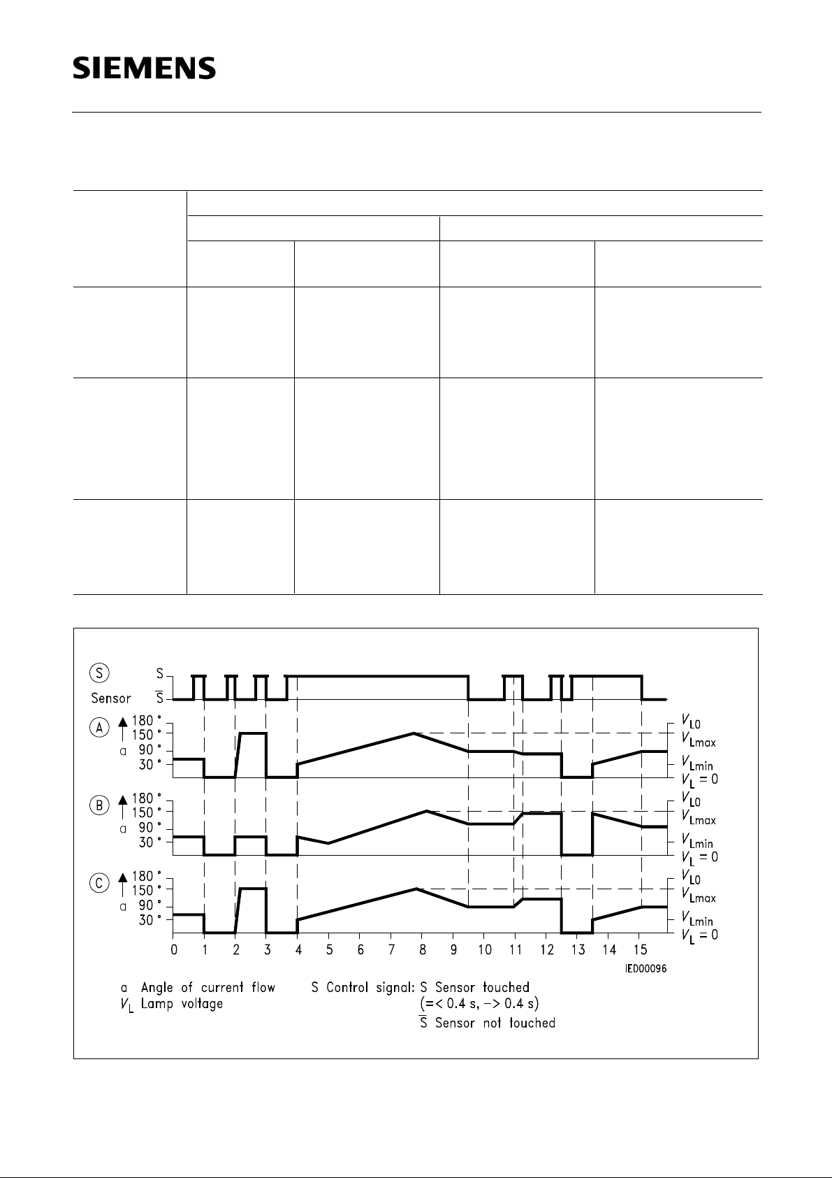
Control Modes of Operation
Mode Period of Touching the Sensor/Extension
Short (60 to 400 ms) Long (more than 400 ms)
SLB 0587
Pre-Touch
A (Pin 2 at V SS) OFF
Max.
Intermediate
B (Pin 2 open) OFF
Max.
Intermediate
C (Pin 2 at V DD) OFF
Max.
Intermediate
Status
Post-Touch
Status
Softstart to Max.
OFF
OFF
Softstart to
stored brightness
from last turn-OFF
OFF
OFF
Softstart to Max.
OFF
OFF
Pre-Touch
Status
OFF
Max./Intermediate
Repeated dimming
OFF
Max./Intermediate
Repeated dimming
OFF
Max./Intermediate
Repeated dimming
Post-Touch
Status
Starts varying at min.
Starts varying at
pre-touch brightness
Same dimming
direction
Softstart to stored
brightness
and varying
Starts varying at
pre-touch brightness
Reversed dimming
direction
Starts varying at min.
Starts varying at
pre-touch brightness
Reversed dimming
direction
Figure 3
Control Behaviour of the 3 Operating Modes
Semiconductor Group 6
Page 7
SLB 0587
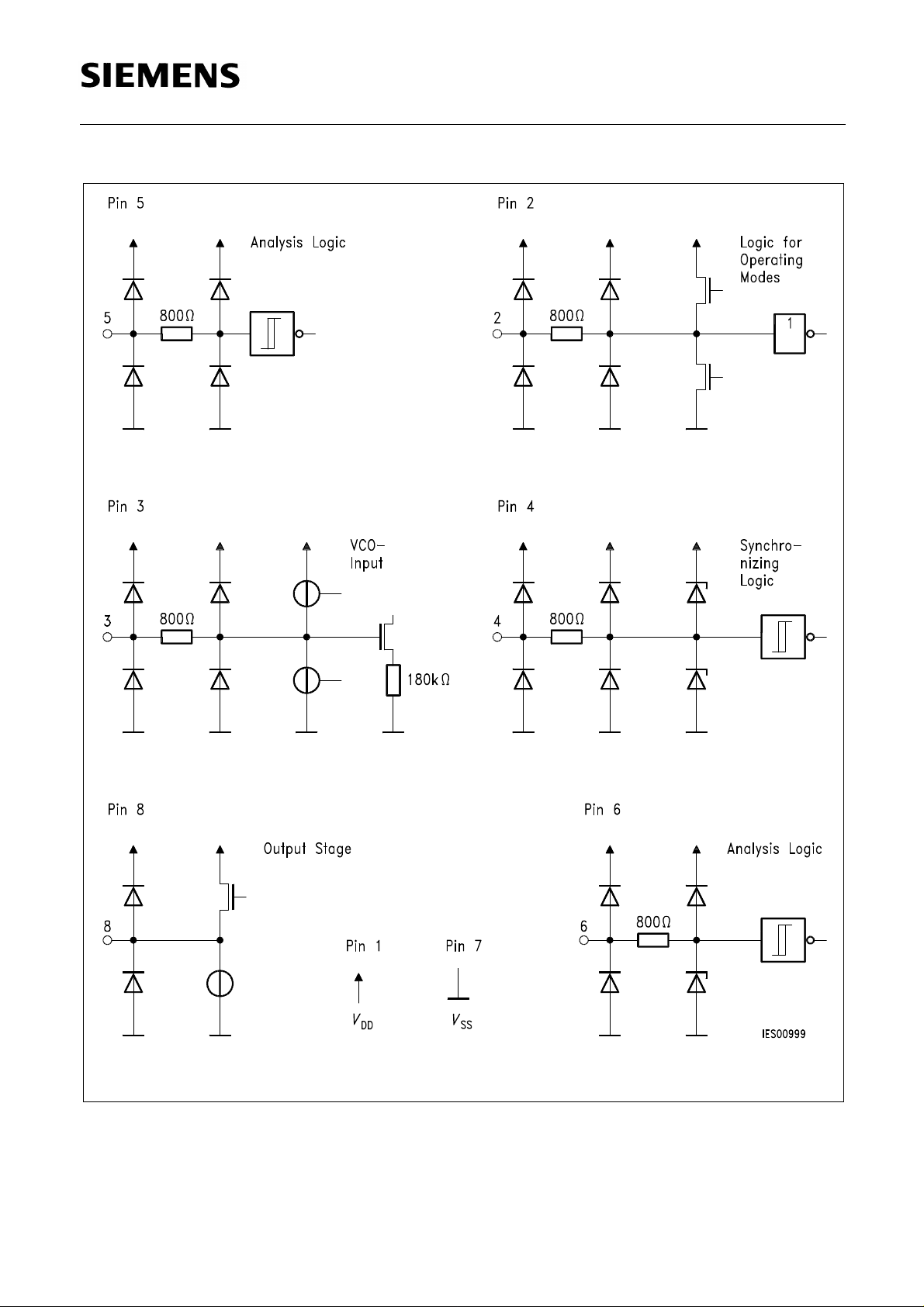
Figure 2
Internal Wiring of Pins
Semiconductor Group 7
Page 8

Interference Immunity
SLB 0587
Components C
3, C 6 and R 3 (figure 4) provide for a stable operating voltage and thus for error-
free working of the circuit, even in the presence of high frequency line interferences (e.g.
caused by cutting in and out of mainly active loads).
In the event of short line interruption (≤ 200 ms) the set circuit state with the external wiring
shown in figure 4 will be maintained. After prolonged line outages (V
S ≤ – 3.6 V) the circuit will
go into the OFF-state.
Upon line outage the synchronization of the internal logic with the line is lost. If the line outage
lasts less than three line cycles, the phasing in of the PLL becomes visible by a brief flickering.
The setting of the PLL can be influenced within certain limits by the selection that is made with
5 and R 10. In general terms, smaller ratings for C 5 and larger ratings for R10 will produce shorter
C
settling times of the PLL.
With more inert PLL characteristics there are slightly better values for rippe-control stability
(visible fluctuations in brightness when operating incandescent lamps and with ripple-control
signal on the line).
If line outages last more than three line cycles, there is blanking for approx. 200 ms after the
line recovers so that the settling process of the PLL is not visible.
Operation of Extensions
Long extension lines in installations cause voltages to be coupled in because of their stray
capacitances and phase capacitances. Internal limiting structures and appropriate evaluating
logic ensure that the circuit can work without interference for stray and phase capacitances up
to 100 nF. Even voltage drops up to 10 V in the phase conductor between the circuit and the
extension button being in phase with the dimming voltage have no effect on the working of the
circuit.
Especially at operation with long extension lines, the RC-network
between pins 3 and 7 (figure 4).
R
10,C5 should be connected
Semiconductor Group 8
Page 9

SLB 0587
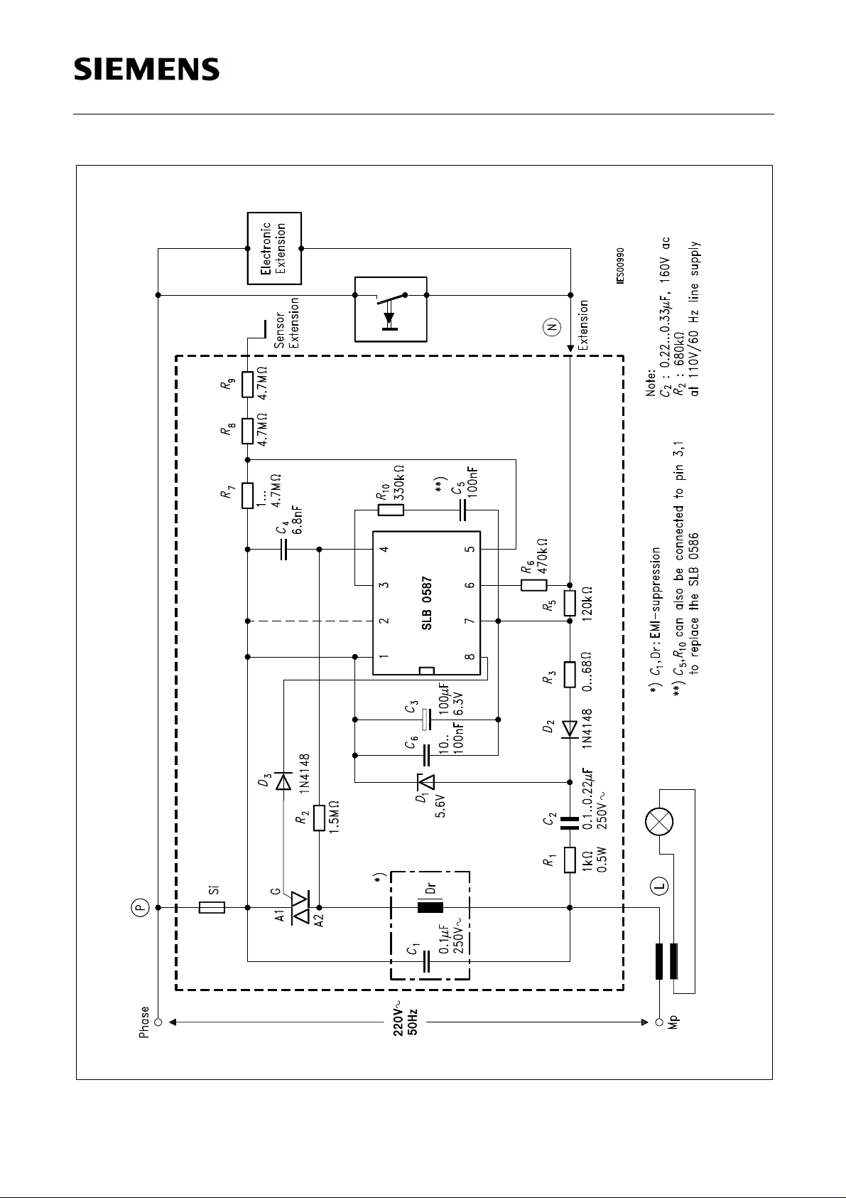
Application Circuit (Figure 4)
The suggested circuit design of the SLB 0587 performs the following functions:
● Current supply for the circuits (R 1, R 3, C 2, C 3, C 6, D1, D2).
● Filtered signal for synchronization of the internal time base (PLL circuit) with line frequency
(
R 2, C 4).
● For specific applications C 4 and R 2 can be varied according to figure 5. An increase for C
4 and R 2 causes a slight reduction of the lamp brightness but at the same time an im-
provement of interference immunity of the internal PLL against line voltage spikes.
● Integration unit for internal PLL circuit (C 5, R 10)
Combining R
– Start-up behaviour of internal PLL after line failure
– Ripple control behaviour (periodic shifts of lamp brightness if ripple control signals
represent)
● Protection of the user (R 8, R 9)
10 and C 5 (figure 6) determines within certain limits the following factors
● Sensitivity setting of the sensor (R 7)
● Current limitation in the case of reverse polarity of the extension (R 5, R 6)
Both resistors can be omitted if no extension is connected. In this case pin 6 must be con-
nected to V
● D3: Reduction of positive voltages which may arise during the triggered state at the gate of
some triacs, to values belowV
SS (pin 7).
DD + 0.3 V by diode forward voltage. If suitable triacs are used,
diode D3 can be omitted.
● Dr,
C
1 are used for EMI suppression.
Depending on the application the EMI suppression is to be dimensioned in acc. with
VDE 0875/part 1 (general)
VDE 0550/part 6 (chokes)
or corresponding the national regulations e.g. 1.4....2 mH, Q = 11....24
Semiconductor Group 9
Page 10
SLB 0587
Figure 4
Application Circuit
Semiconductor Group 10
Page 11
Application Notes
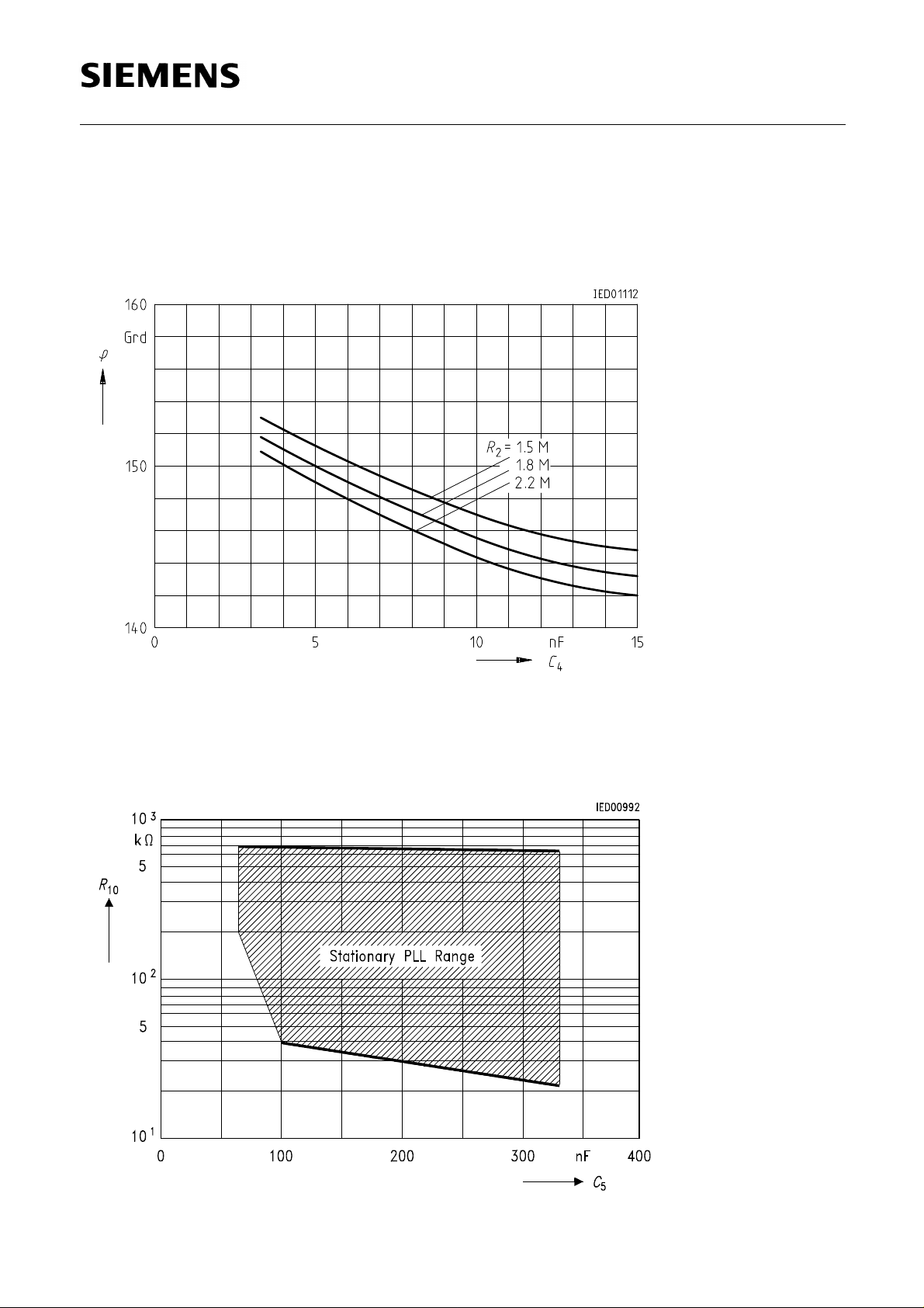
Figure 5
Dependence of C
SLB 0587
4 and maximum Angle of Current Flow
*) The capacitor value of C 4 is limited to max. 12 nF for a line frequency of 60 Hz.
Figure 6
Range of Value of the RC-Component at Pin3 for Stationary PLL-Operation
Semiconductor Group 11
Page 12
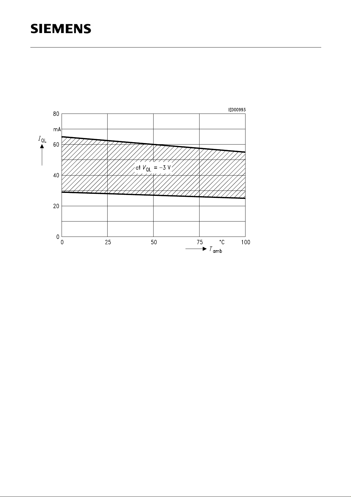
Figure 7
Range of Value for Trigger Current of Pin 8 over Temperature Range
SLB 0587
Semiconductor Group 12
Page 13
SLB 0587
Operation of Control Inputs
All switching and control functions can also be performed from extensions which are connected to the extension input. The main sensor input and the extension inputs have equal
priority. Electronic sensor switches or mechanical pushbutton switches can be connected to
the extensions.
Input potential during both half waves of the line phase:
Line Half Wave Sensor InputFunction Extension Input
positive LOperated
negative don’t careNot operated
H
positive HOperated
negative don’t careNot operated
Functional Description of the Evaluation Logic for Sensor and Extension Inputs
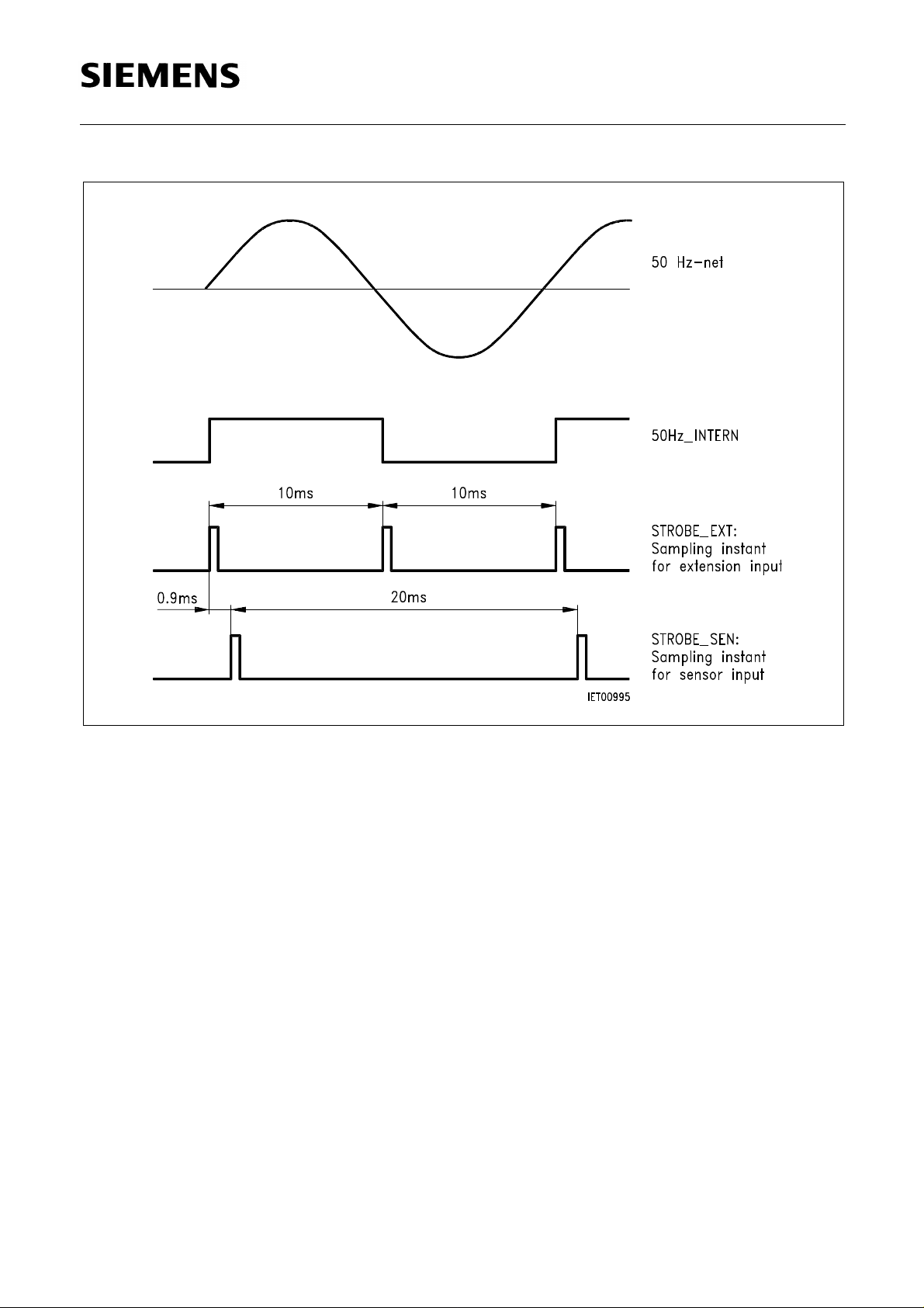
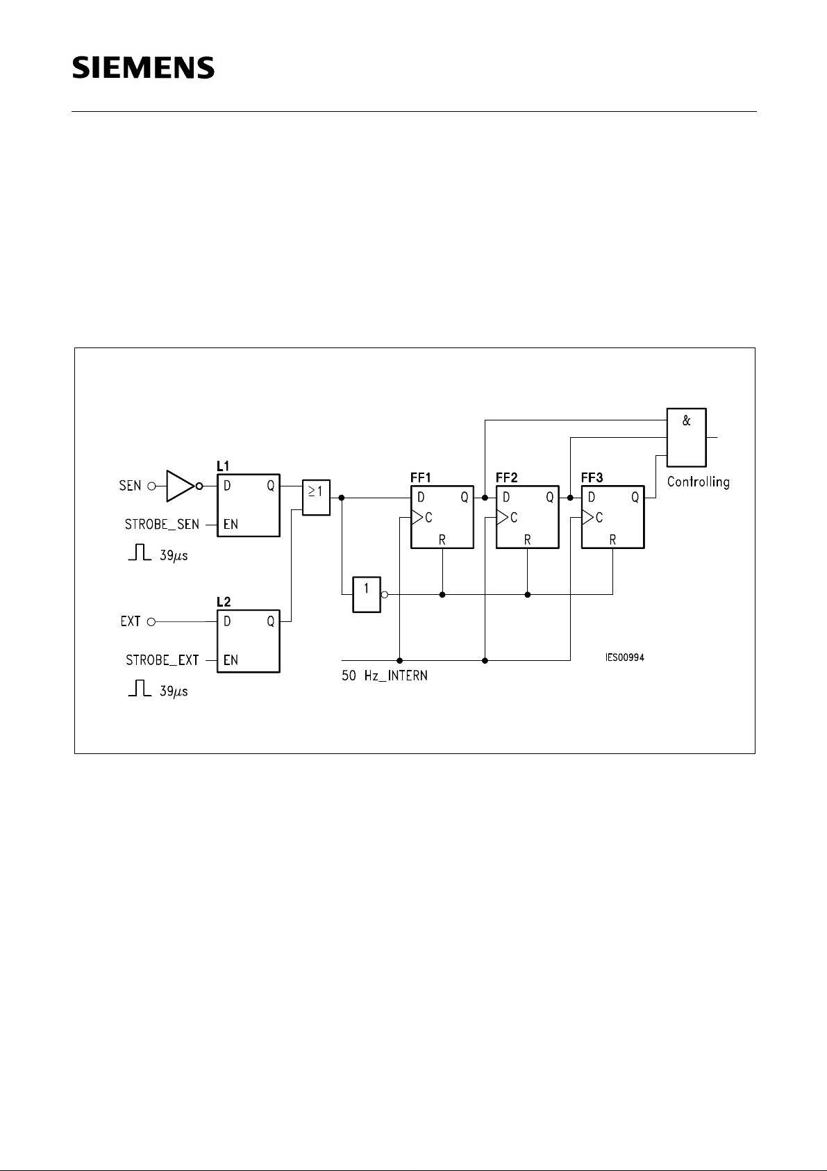
The logic levels at the sensor and extension inputs are sampled by latches L1 and L2 using
the timing pattern shown in the timing diagram of figure 8.
For operation (ON/OFF or change of brightness) flipflops FF1 to FF3 must be "1".
Minimum ON/OFF Times
Extension Input: approx. 40 to 60 ms
Sensor Input: approx. 40 to 60 ms
L
don’t care L
or
don’t care
Semiconductor Group 13
Page 14
SLB 0587
Figure 8
Timing Diagram of the Evaluation Logic for the Sensor and Extension Inputs
Semiconductor Group 14
Page 15
SLB 0587
Wireless Remote Control
The connection of a wireless remote control to the extension is very easy. All functions of the
SLB 0587 can be performed with the aid of a single transfer channel.
General Information
All time specifications refer to a line frequency of 50 Hz. In case of a line frequency of 60 Hz,
the times are reduced accordingly.
Figure 9
Circuit Principle of the Evaluation Logic for the Sensor and Extension Inputs
Semiconductor Group 15
Page 16
SLB 0587
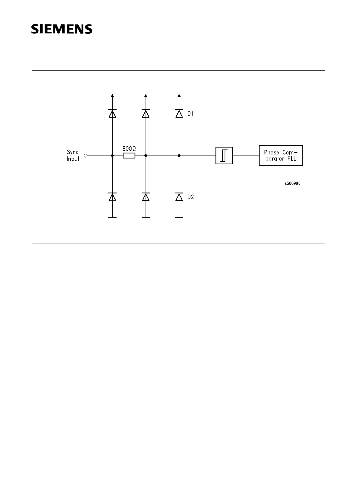
Figure 10
Circuit Principle at the Sync Input
Functional Description
Diodes D1 and D2 exhibit a behaviour similar to that of a Z-diode and become conductive at
approx. 3.0 V.
R
Despite of the line voltage at the triac, it is ensured in combination with
2 (figure 4) that the
voltages occuring at the sync input of the SLB 0587 do not exceed essentially the range of the
supply voltage.
Semiconductor Group 16
Page 17
SLB 0587
Figure 11
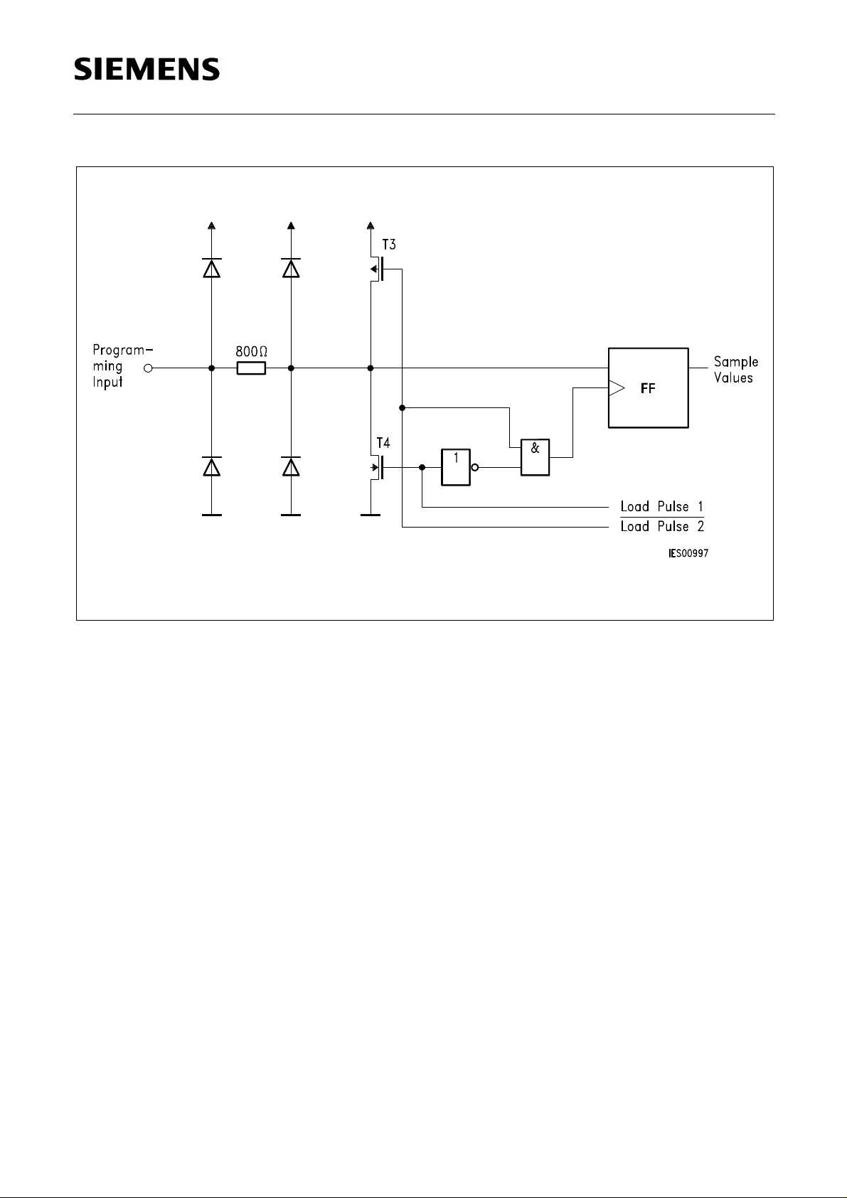
Circuit Principle on Programming Input (Pin 2)
Functional Description of the Programming Input (Pin 2):
The SLB 0587 distinguishes between 3 operating modes if pin 2 is wired accordingly.
The transistors T3 and T4 alternate in being conductive as shown in figure 11.
Acceptance of the logic level (which is dependent on the external wiring of the input) at the programming input, is performed during the second edge of the load pulse.
Semiconductor Group 17
Page 18
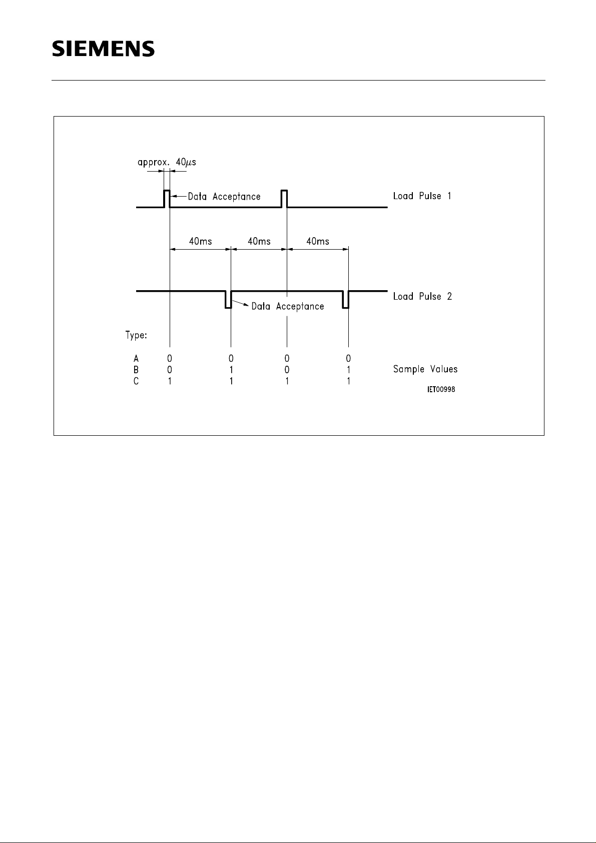
SLB 0587
Figure 12
Internal Timing for Distinguishing between the Operating Modes A, B and C
Semiconductor Group 18
Page 19
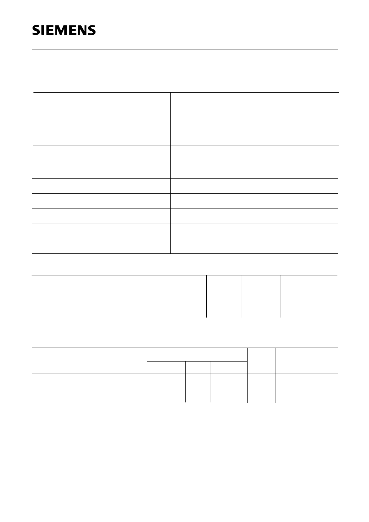
Absolute Maximum Ratings
DD =0 V
V
SLB 0587
Parameter Symbol
Input current:
Sync input
Extension input
I
I
I I
Total power dissipation (T A = 25 °C)
Thermal resistance
System-air (P-DIP-8)
System-air (P-DSO-8-1)
th SA
R
R th SA
Operating Range
UnitLimit Values
min. max.
– 7.5 0.3Supply voltage V SS V
V S – 0.3 0.3Input voltage V I V
– 0.5
–1
0.5
1
mA
mA
125Junction temperature T j °C
– 55 125Storage temperature T stg °C
10 mW
135
231
K/W
K/W
Characteristics
T
A = 25 °C; V SS = –5 V (V DD = 0 V)
Parameter Symbol
Quiescent current,
DD mA0.5 0.65
I
pin 1
– 5.6 – 4.5Supply voltage V SS V
47.5 63Line frequency f Hz
0 100Ambient temperature T A °C
min. max.
typ.
Unit Test ConditionLimit Values
Dimmer OFF:
fsync =50 Hz
R
L = 120 Ω
*)
*)
Load resistance between pin 1 and pin 8
Semiconductor Group 19
Page 20
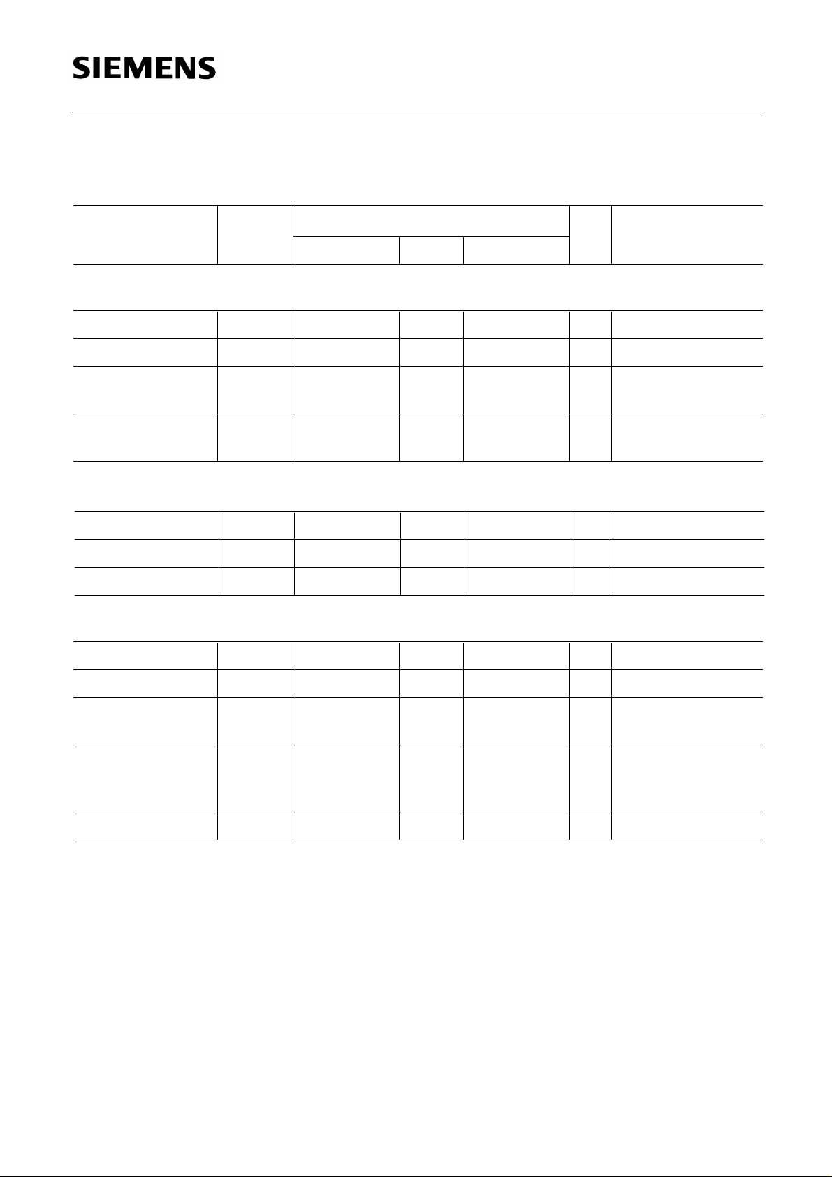
Characteristics (cont’d)
A =25 °C; V SS = – 5 V (VDD =0 V)
T
SLB 0587
Parameter Symbol
Sensor Input (pin 5)
H-input voltage
L-input voltage
Input current
V IH
V IL
I IH
(extension)
Input current
I IH
I IL
Extension (pin 6)
H-input voltage
L-input voltage
Input current
V IH
V IL
I IL
Sync Input (pin 4)
min. max.
typ.
1/2 V SS + 1.1
1/2 V SS – 1.1
23
–1
0
0
1
V SS + 3.0
V SS + 0.8
0
1
Unit Test ConditionLimit Values
V
V
µA
220 V at sensor
(extension)
µA
V I = 0 V
µA
I = V SS
V
V
V
µA V I = V SS
H-input voltage
L-input voltage
Input current
HL transition time
(trigger transition)
LH transition time
Frequency
V IH
V IL
I IH
t THL
t TLH
f
1/2 VSS + 1.8
207
supply
sine
wave
50/60
1/2 V SS + 1.8VV
µA
Hz
Application
Circuit
Line frequency
Semiconductor Group 20
Page 21
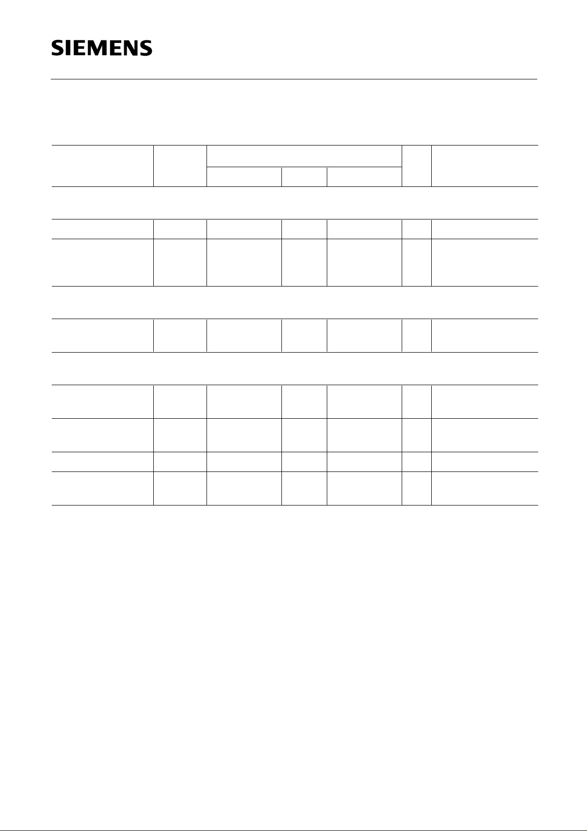
Characteristics (cont’d)
A =25 °C; V SS = – 5 V (VDD =0 V)
T
SLB 0587
Parameter Symbol
Programming Input (pin 2)
Load capacitance
C L
Load resistance
Mode B
Mode A; C
R L
R L
Integrator (pin 3)
Application circuit C 5
R 10
Output (pin 8)
L-output current
L-pulse width
I OL
t QL
min. max.
0
200
0
68
22
25
typ.
100
330
500
∞
1
330
680
65
117.2
97.7
Unit Test ConditionLimit Values
pF
kΩ
kΩ
nF
Ω
k
mA
µs
µs
see figure 4
V QL = – 3 V
L = 120 Ω
R
50 Hz supply
60 Hz supply
HL transition time
LH transition time
t HLQ
t HLQ
200
1
ns
µs
R L = 120 Ω
C L = 1 nF
Semiconductor Group 21
Page 22
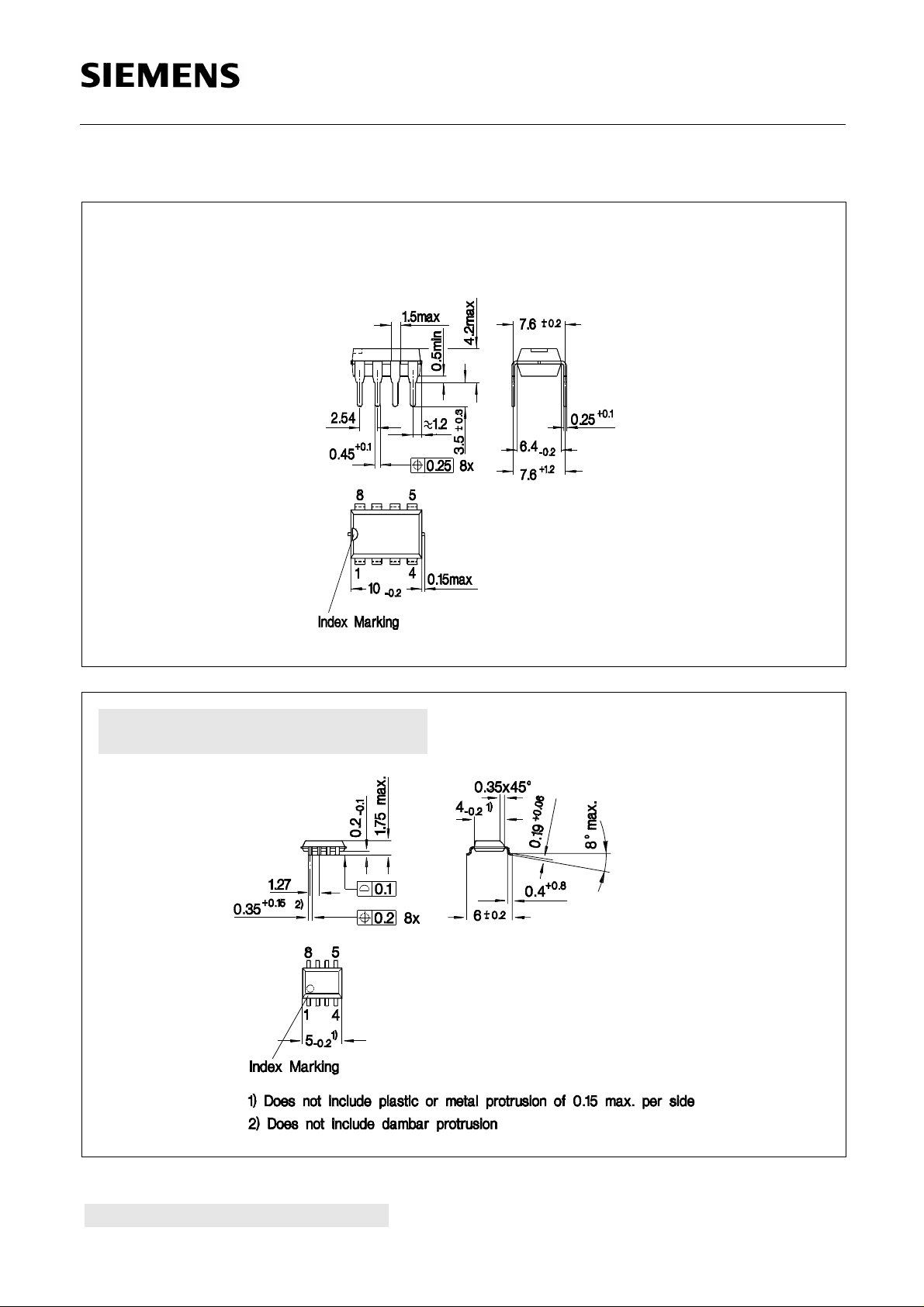
Package Outlines
Plastic Package, P-DIP-8
(Plastic Dual In-Line Package)
SLB 0587
Plastic Package, P-DSO-8-1 (SMD)
(Plastic Dual Small Outline)
SMD = Surface Mounted Device Dimensions in mm
Semiconductor Group 22
 Loading...