

Page 1
S6A0031
Contents in this document are subject to change without notice. No part of this document may be reproduced or
for any purpose, without the express written
permission of LCD Driver IC Team.
8 COM / 80 SEG DRIVER & CONTROLLER FOR STN LCD
June. 1999.
Ver. 0.5
Prepared by: Tae-Kwang, Park
parktk@samsung.co.kr
transmitted in any form or by any means, electronic or mechanical,
Page 2

Page 3

S6A0031 Specification Revision History
Version Content Date
0.0 Original Feb.1999
0.1
ECKON pad added
POR circuit added
Page 6: E_RD signal description is changed
E_RD: Active low signal for writing command in 6800 mode or high enable
0.2
signal for reading command in 8080 mode. →
E_RD: Active low signal for writing command or high enable signal for reading
command in 6800 mode, low enable signal for reading command in
8080 mode.
Page 6: LCD DRIVER OUTPUT added
Page 18: Power ON / OFF timing added
0.3
Page 29: I
Page 30: I
(VDD = 2.4~3.6V): 150µA → 50µA
DD1
(VDD = 3.6~5.5V): 250µA → 80µA
DD1
0.4 Page 1, 2, 11: CGROM character size is changed from 256 to 254. Jun.1999
Page 6: RW_WR active low -> active high
0.5
Page 6: RW_WR active low -> low enable
Page 20: Wait for more than 1.2us or Busy Check -> delete “or Busy Check”
Page 21: Wait for more than 1.2us or Busy Check -> delete “or Busy Check”
Mar.1999
Apr.1999
May.1999
Jun.1999
Page 4

S6A0031 PRELIMINARY SPEC. VER. 0.5 8 COM / 80 SEG DRIVER & CONTROLLER FOR STN LCD
CO
NTENTS
INTRODUCTION.......................................................................................................................................... 1
FEATURES ................................................................................................................................................. 1
BLOCK DIAGRAM ...................................................................................................................................... 2
PAD CONFIGURATION............................................................................................................................... 3
PAD CENTER COORDINATES...................................................................................................................4
PIN DESCRIPTION...................................................................................................................................... 5
POWER SUPPLY.................................................................................................................................5
SYSTEM CONTROL............................................................................................................................. 5
MPU INTERFACE ................................................................................................................................ 6
LCD DRIVER OUTPUT......................................................................................................................... 6
TEST....................................................................................................................................................6
FUNCTIONAL DESCRIPTION.....................................................................................................................7
MICROPROCESSOR INTERFACE ...................................................................................................... 7
ADDRESS COUNTER (AC)................................................................................................................ 10
DISPLAY DATA RAM (DDRAM)......................................................................................................... 10
CHARACTER GENERATOR ROM (CGROM)..................................................................................... 11
CHARACTER GENERATOR RAM (CGRAM) ..................................................................................... 12
LCD DRIVER CIRCUIT....................................................................................................................... 13
INSTRUCTION DESCRIPTION.................................................................................................................. 14
INITIALIZING............................................................................................................................................. 18
HARDWARE RESET.......................................................................................................................... 18
INSTRUCTION INITIALIZING WITH RESET....................................................................................... 20
LCD DRIVING POWER SUPPLY CIRCUIT................................................................................................ 22
MPU INTERFACE...................................................................................................................................... 23
INTERFACING WITH 8080-SERIES MICROPROCESSORS.............................................................. 23
INTERFACING WITH 6800-SERIES MICROPROCESSORS.............................................................. 23
APPLICATION INFORMATION FOR LCD PANEL.................................................................................... 24
FRAME FREQUENCY............................................................................................................................... 26
MAXIMUM ABSOLUTE RATE................................................................................................................... 27
ELECTRICAL CHARACTERISTICS.......................................................................................................... 28
DC CHARACTERISTICS.................................................................................................................... 28
AC CHARACTERISTICS.................................................................................................................... 30
2
Page 5
8 COM / 80 SEG DRIVER & CONTROLLER FOR STN LCD PRELIMINARY SPEC. VER. 0.5 S6A0031
INTRODUCTION
This character driver and controller LSI for liquid crystal dot matrix display systems can display 1-line of 16
characters with the 5 x 8 dots format. It is capable of interfacing various microprocessors, supporting the 4-bit or
8-bit parallel mode. Voltage follower and bias circuit is built in the IC.
FEATURES
Driver Output Circuits
− 8 common outputs / 80 segment outputs
Applicable Duty Ratio
Font size Display size Duty Contents of outputs
5 x 8 1-line x 16 characters 1/8 1 x 16 characters
On-chip Display Data RAM
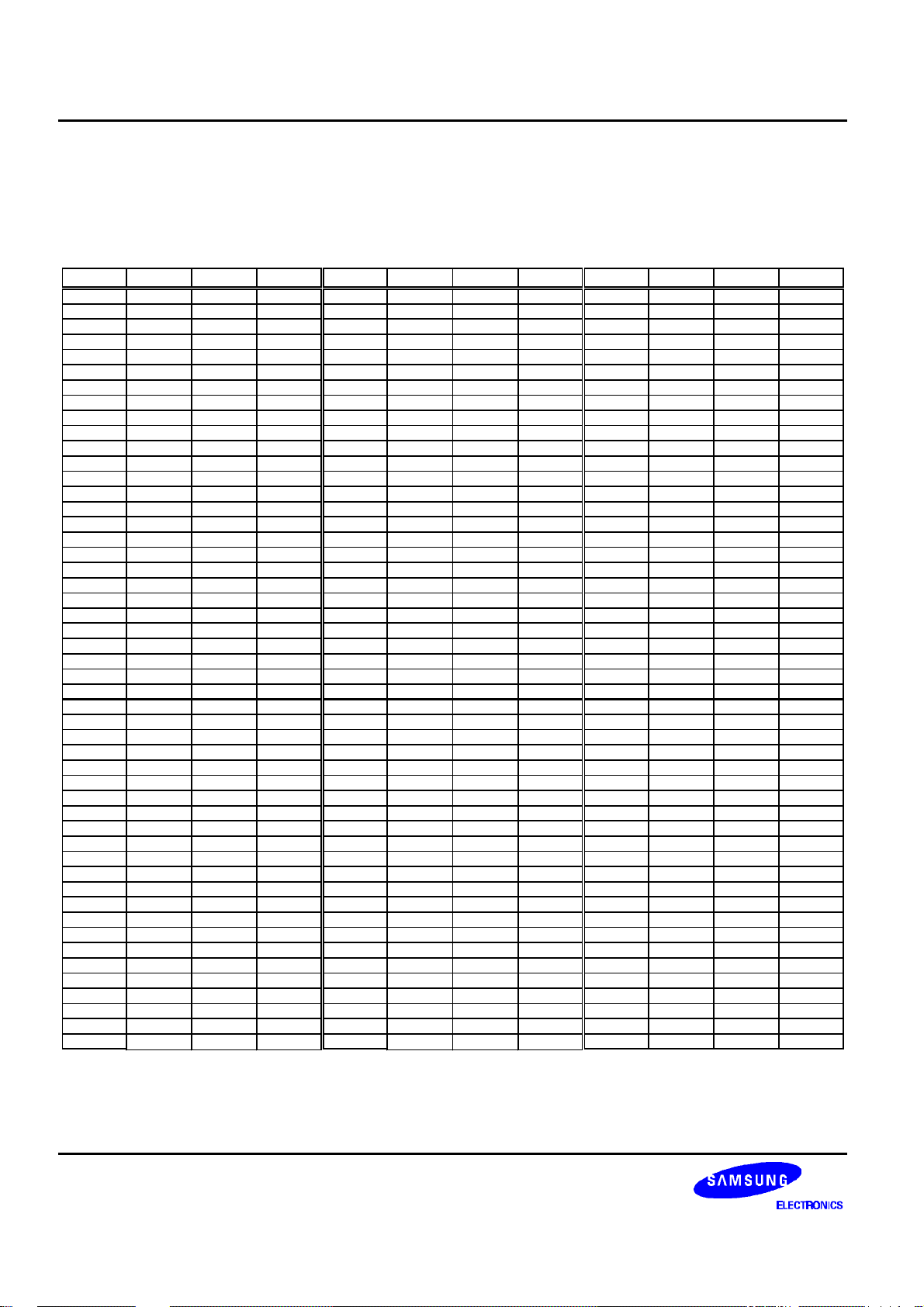
− Character Generator ROM (CGROM): 10,160 bits (254 characters x 5 x 8 dots)
− Character Generator RAM (CGRAM): 80 bits (2 characters x 5 x 8 dots)
− Display Data RAM (DDRAM): 256 bits (16 characters x 1-line + 16 extended characters)
Microprocessor Interface
− 8-bit parallel interface with 6800-series or 8080-series MPU
− 4-bit parallel interface with 6800-series or 8080-series MPU
Function Set
− Simple instruction set
− COM / SEG bi-directional (4 types LCD application available)
− Hardware reset (RESETB)
On-chip Analog Circuit
− Internal RC oscillator circuit
− Voltage follower & bias circuit
− Automatic power on reset circuit
Operating Voltage Range
− Supply voltage (VDD): 2.4 to 5.5 V
− LCD driving voltage (VLCD = V0 - VSS): 6.0V Max.
Low Power Consumption
Package Type
− Gold bumped chip
1
Page 6
S6A0031 PRELIMINARY SPEC. VER. 0.5 8 COM / 80 SEG DRIVER & CONTROLLER FOR STN LCD
DB4
DIRC
CK
555
8
8
(OR)
MI
ECKON
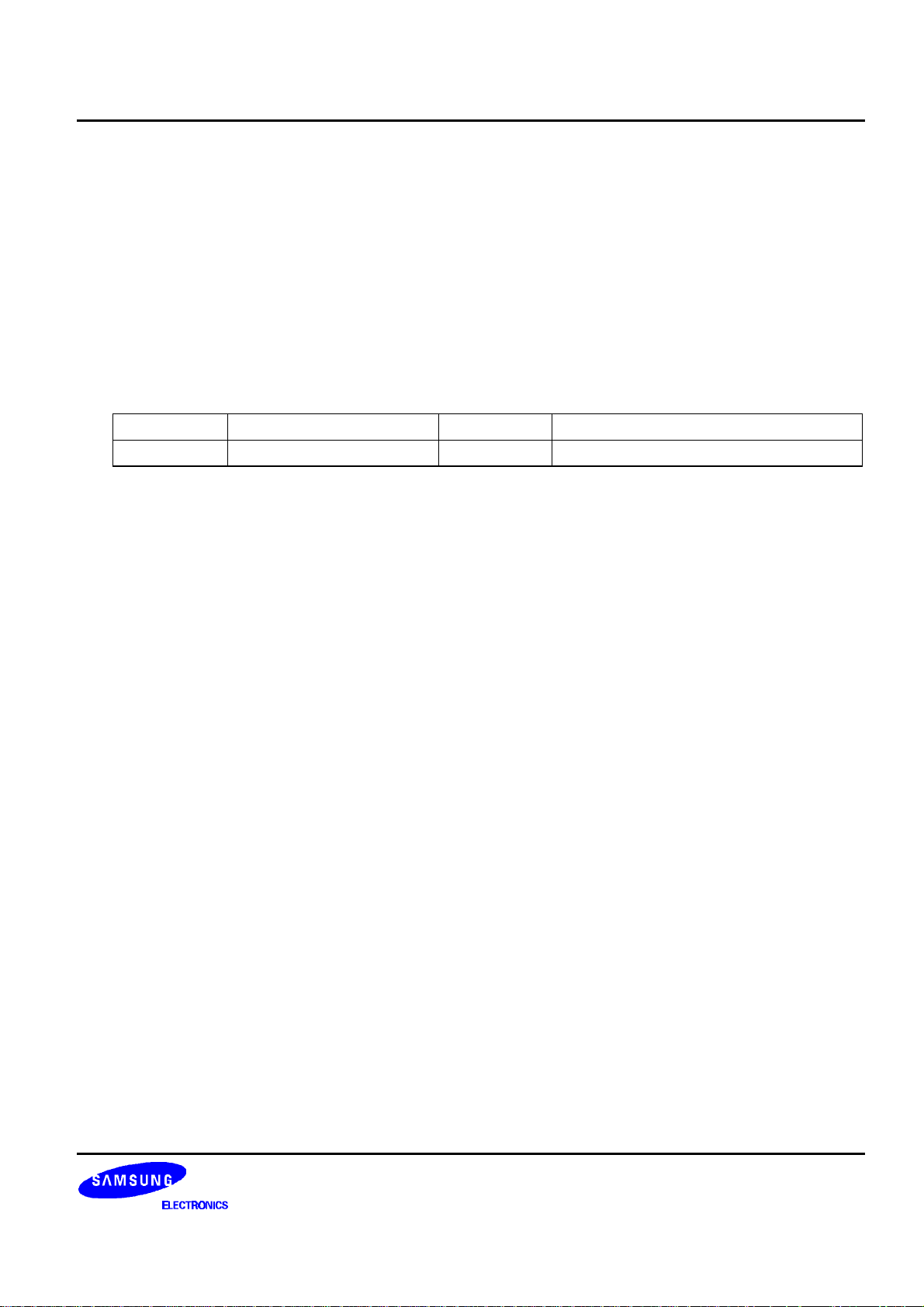
BLOCK DIAGRAM
Power On
Reset (POR)
RESETB
CSB
RS
RW_WR
E_RD
DB7 to
DB3 to
DB0
Input Buffer
Parallel
Interface
4 bit/8 bit
(6800/8080
-series)
Instruction
8
Register
8
Register
Data Output
8
Register
(IR)
Data
(DR)
Address
Counter
Instruction
Decoder
Display
Data RAM
(DDRAM)
256 bits
Timing GeneratorOscillator
8 bits
Shift
Register
80 bits
8
Shift
Register
80 bits
Latch
Circuit
Common
Driver
Segment
Driver
COM1 to
COM8
SEG1 to
SEG80
DD
V
GND
Busy
Flag
Character
Generator
RAM
(CGRAM)
80 bits
5 5
Segment Data Conversion
Character
Generator
ROM
(CGROM)
10,160 bits
Figure 1. Block Diagram
Cursor
and
Blink
Controller
DIRS
LCD Driving
Voltage Selector
Voltage Follower
& Bias Resistor
V0 V1 V2 V3 V4
2
Page 7
8 COM / 80 SEG DRIVER & CONTROLLER FOR STN LCD PRELIMINARY SPEC. VER. 0.5 S6A0031
1
44
60
129
5352136
S6A0031
(+2600, +590)
(-2600, +605)
30
µ
m
30
µ
m
30
µ
m
60
µ
m
30
µ
m
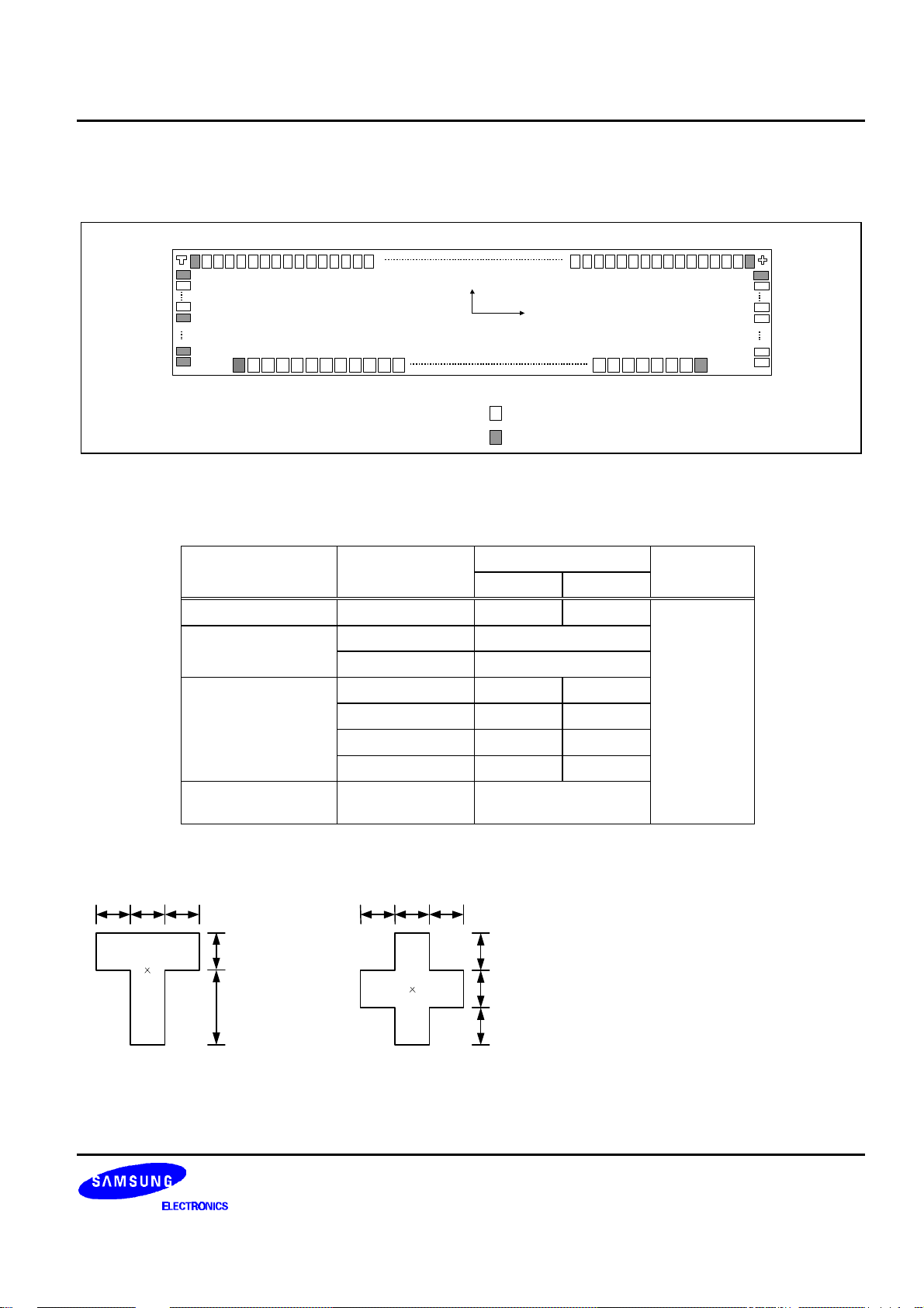
PAD CONFIGURATION
z
130
137
144
Y
(0,0)
X
PAD
DUMMY_PAD
Figure 2. S6A0031 Chip Configuration
Table 1. S6A0031 Pad Dimensions
Item Pad No.
Size
X Y
Chip size - 5430 1410
Pad pitch
1 to 44 90
45 to 144 70
1 to 44 52 92
Bumped pad size
45 to 59 92 42
60 to 129 42 92
130 to 144 92 42
59
45
Unit
µm
Bumped pad height
1 to 144 17 (Typ.)
COG Align Key Coordinate
30µm 30µm 30µm
3
30µm 30µm 30µm
Page 8
S6A0031 PRELIMINARY SPEC. VER. 0.5 8 COM / 80 SEG DRIVER & CONTROLLER FOR STN LCD
50
COM6
2605
-205
100
SEG46
-385
595
150
PAD CENTER COORDINATES
Table 2. Pad Center Coordinates
[Unit: µm]
No. Name X Y No. Name X Y No. Name X Y
1 DUMMY -1935 -595 51 COM7 2605 -135 101 SEG47 -455 595
2 VSS -1845 -595 52 COM8 2605 -65 102 SEG48 -525 595
3 VSS -1755 -595 53 SEG1 2605 5 103 SEG49 -595 595
4 VSS -1665 -595 54 SEG2 2605 75 104 SEG50 -665 595
5 ECKON -1575 -595 55 SEG3 2605 145 105 SEG51 -735 595
6 VDD -1485 -595 56 SEG4 2605 215 106 SEG52 -805 595
7 V4 -1395 -595 57 SEG5 2605 285 107 SEG53 -875 595
8 V3 -1305 -595 58 SEG6 2605 355 108 SEG54 -945 595
9 V2 -1215 -595 59 DUMMY 2605 425 109 SEG55 -1015 595
10 V1 -1125 -595 60 DUMMY 2415 595 110 SEG56 -1085 595
11 CK -1035 -595 61 SEG7 2345 595 111 SEG57 -1155 595
12 VDD -945 -595 62 SEG8 2275 595 112 SEG58 -1225 595
13 VDD -855 -595 63 SEG9 2205 595 113 SEG59 -1295 595
14 VDD -765 -595 64 SEG10 2135 595 114 SEG60 -1365 595
15 V0 -675 -595 65 SEG11 2065 595 115 SEG61 -1435 595
16 V0 -585 -595 66 SEG12 1995 595 116 SEG62 -1505 595
17 VDD -495 -595 67 SEG13 1925 595 117 SEG63 -1575 595
18 VDD -405 -595 68 SEG14 1855 595 118 SEG64 -1645 595
19 VDD -315 -595 69 SEG15 1785 595 119 SEG65 -1715 595
20 RESETB -225 -595 70 SEG16 1715 595 120 SEG66 -1785 595
21 RS -135 -595 71 SEG17 1645 595 121 SEG67 -1855 595
22 RW_WR -45 -595 72 SEG18 1575 595 122 SEG68 -1925 595
23 VSS 45 -595 73 SEG19 1505 595 123 SEG69 -1995 595
24 E_RD 135 -595 74 SEG20 1435 595 124 SEG70 -2065 595
25 VDD 225 -595 75 SEG21 1365 595 125 SEG71 -2135 595
26 DB0 315 -595 76 SEG22 1295 595 126 SEG72 -2205 595
27 DB1 405 -595 77 SEG23 1225 595 127 SEG73 -2275 595
28 DB2 495 -595 78 SEG24 1155 595 128 SEG74 -2345 595
29 DB3 585 -595 79 SEG25 1085 595 129 DUMMY -2415 595
30 DB4 675 -595 80 SEG26 1015 595 130 DUMMY -2605 425
31 DB5 765 -595 81 SEG27 945 595 131 SEG75 -2605 355
32 DB6 855 -595 82 SEG28 875 595 132 SEG76 -2605 285
33 DB7 945 -595 83 SEG29 805 595 133 SEG77 -2605 215
34 CSB 1035 -595 84 SEG30 735 595 134 SEG78 -2605 145
35 VSS 1125 -595 85 SEG31 665 595 135 SEG79 -2605 75
36 MI 1215 -595 86 SEG32 595 595 136 SEG80 -2605 5
37 VDD 1305 -595 87 SEG33 525 595 137 DUMMY -2605 -65
38 TEST 1395 -595 88 SEG34 455 595 138 DUMMY -2605 -135
39 VSS 1485 -595 89 SEG35 385 595 139 DUMMY -2605 -205
40 DIRC 1575 -595 90 SEG36 315 595 140 DUMMY -2605 -275
41 VDD 1665 -595 91 SEG37 245 595 141 DUMMY -2605 -345
42 DIRS 1755 -595 92 SEG38 175 595 142 DUMMY -2605 -415
43 VSS 1845 -595 93 SEG39 105 595 143 DUMMY -2605 -485
44 DUMMY 1935 -595 94 SEG40 35 595 144 DUMMY -2605 -555
45 COM1 2605 -555 95 SEG41 -35 595 145
46 COM2 2605 -485 96 SEG42 -105 595 146
47 COM3 2605 -415 97 SEG43 -175 595 147
48 COM4 2605 -345 98 SEG44 -245 595 148
49 COM5 2605 -275 99 SEG45 -315 595 149
4
Page 9
8 COM / 80 SEG DRIVER & CONTROLLER FOR STN LCD PRELIMINARY SPEC. VER. 0.5 S6A0031
, External clock by CK pin is used as system clock, and internal
PIN DESCRIPTION
POWER SUPPLY
Table 3. Pin Description
Name I/O Description
VDD Supply Power supply
VSS Supply Ground
V0 I Bias voltage Input for LCD driving
LCD driving voltage outputs.
Voltages should have the following relationship;
V1
V2
V3
V4
O
V0 ≥ V1 ≥ V2 = V3 ≥ V4 ≥ VSS
These voltages are generated as following table.
LCD bias V1 V2 V3 V4
1/4 bias (3/4) x V0 (2/4) x V0 (1/4) x V0
SYSTEM CONTROL
Table 3. Pin Description (Continued)
Name I/O Description
Clock source selection input
ECKON I
CK I
MI I
DIRC I
DIRS I
When ECKON = "High"
oscillator circuit is turned OFF. When ECKON = "Low", internal oscillator is used.
External clock input (when ECKON = "High")
It must be fixed "High" or "Low" when the internal oscillation circuit is used (When
ECKON = "Low").
MPU interface selection input
MI = "Low", 8080-series MPU
MI = "High", 6800-series MPU
COM direction selection input
When DIRC = "Low"
COM1 → COM2 - - - - → COM7 → COM8
When DIRC = "High"
COM8 → COM7 - - - - → COM2 → COM1
SEG direction selection input
When DIRS = "Low"
SEG1 → SEG2 - - - - → SEG79 → SEG80
When DIRS = "High"
SEG80 → SEG79 - - - - → SEG2 → SEG1
5
Page 10
S6A0031 PRELIMINARY SPEC. VER. 0.5 8 COM / 80 SEG DRIVER & CONTROLLER FOR STN LCD
MPU INTERFACE
Table 3. Pin Description (Continued)
Name I/O Description
RESETB I
CSB I
RS I
RW_WR I
E_RD I
DB0 to DB3
DB4 to DB7
I/O
Reset input
Initialization is performed by "Low" level sensing of the RESETB signal.
Chip selection input
S6A0031 is selected while CSB is "Low".
Register selection input
When RS = "Low", instruction register
When RS = "High", data register
In 8080-series MPU interface mode, this pin is connected to WR pin of MPU and is an
active high write signal.
In 6800-series MPU interface mode, this pin is connected to R/W pin of MPU.
When RW_WR = "High", read mode
When RW_WR = "Low", write mode
In 8080-series MPU interface mode, this pin is connected to RD pin of MPU and is a low
enable read signal.
In 6800-series MPU interface mode, this pin is connected to E pin of MPU and enables
read or write command according to RW_WR signal.
When 8-bit interface mode, used as bi-directional data bus DB0 to DB7
During 4-bit bus mode, only DB4 to DB7 are used. In this case DB0 - DB3 pins are
don’ t care (connect to "High", "Low" or open).
LCD DRIVER OUTPUT
Table 3. Pin Description (Continued)
Name I/O Description
COM1 to
COM8
SEG1 to
SEG80
O Common signal output for character display
O Segment signal output for character display
TEST
Table 3. Pin Description (Continued)
Name I/O Description
TEST I
*NOTE: DUMMY – These pins should be opened (floated).
6
Test pin
This pin is not used for normal operation and should be connect to "Low".
Page 11
8 COM / 80 SEG DRIVER & CONTROLLER FOR STN LCD PRELIMINARY SPEC. VER. 0.5 S6A0031
FUNCTIONAL DESCRIPTION
MICROPROCESSOR INTERFACE
S6A0031 has two kinds of interface type with MPU: 4-bit bus or 8-bit bus. 4-bit bus and 8-bit bus is selected by the
DL bit in the instruction register, and 6800-series MPU or 8080-series MPU is selected by MI pin.
Table 4. Various Kinds of MPU Interface according to MI and DL Bit
MI DL CSB RS
6800-series
(H)
8080-series
(L)
NOTE: "-" - Don’t care ("High", "Low" or Open)
(H): fixed "High" (VDD)
(L): fixed "Low" (VSS)
MI: "High" = 6800-series MPU, "Low" = 8080-series MPU
DL: "High" = 8-bit mode, "Low" = 4-bit mode
CSB: "High" = chip is not selected, "Low" = chip is selected
RS: "High" = data register, "Low" = instruction register
RW_WR: Read / Write indicating signal in 6800 mode, active high signal for writing command in 8080 mode.
E_RD: Active low signal for writing command or high enable signal for reading command in 6800 mode,
low enable signal for reading command in 8080 mode.
Parallel Interface
During writing operation, two 8-bit registers, data register (DR) and instruction register (IR), are used. The data
register (DR) is used as temporary data storage place for being written into DDRAM / CGRAM. Target RAM is
selected by RAM address set instruction. The Instruction register (IR) is used only to store instruction code
transferred from MPU. To select DR or IR register, RS input pin is used.
8-bit (H) CSB RS R/W E DB0 to DB3 DB4 to DB7
4-bit (L) CSB RS R/W E - DB4 to DB7
8-bit (H) CSB RS WR RD DB0 to DB3 DB4 to DB7
4-bit (L) CSB RS WR RD - DB4 to DB7
RW_WR
E_RD DB0 to DB3 DB4 to DB7
During reading operation, 8-bit output data register (OR) is used. The output data register (OR) is used as temporary
data storage place for being read from DDRAM / CGRAM. Destination RAM is selected by RAM address set
instruction. After RAM address set, the first reading in the 8-bit bus mode (first and second reading in the 4-bit bus
mode) is a dummy cycle (figure 3, 4, 5, 6). The valid data comes from the second reading in the 8-bit bus mode (from
the 3rd reading in 4-bit bus mode). The dummy cycle makes the address counter (AC) indicate the correct address.
So it is recommended to set address before writing. The instruction read operation is supported for indicating
internal operation is being processed (Busy Flag).
In the 4-bit bus mode, it is needed to transfer 4-bit data (through DB4 to DB7) by two times. The high order bits (for
8-bit mode DB4 to DB7) are transferred before the low order bits (for 8-bit mode DB0 to DB3) in read and write
transaction. The DB0 to DB3 pins are floated in this 4-bit bus mode.
After RESETB operation, S6A0031 considers the first 4-bit data from MPU as the high order bits in the 4-bit bus
mode.
7
Page 12
S6A0031 PRELIMINARY SPEC. VER. 0.5 8 COM / 80 SEG DRIVER & CONTROLLER FOR STN LCD
Instruction
Data
Busy Flag
Dummy
Valid
Data
Instruction
Data
Busy flag
Dummy
Valid
Data
DL
MI
CSB
RS
RW_WR
E_RD
DB7 to DB0
Valid
Write
Read
Data Read
Data Read
Write
Figure 3. Timing Diagram of 8-bit Parallel Bus Mode Data Transfer (6800-series MPU Mode)
DL
MI
CSB
RS
RW_WR
E_RD
DB7 to DB0
Write
Read
Data Read
Valid
Data Read
Write
Figure 4. Timing Diagram of 8-bit Parallel Bus Mode Data Transfer (8080-series MPU Mode)
8
Page 13

8 COM / 80 SEG DRIVER & CONTROLLER FOR STN LCD PRELIMINARY SPEC. VER. 0.5 S6A0031
Instruction Write
Busy Flag &
Dummy
Valid
Data Write
Instruction Write
Busy Flag &
Dummy
Valid
Data Write
A0
4-bit
D4
D0
D0
D4
4-bit
DL
MI
CSB
RS
RW_WR
E_RD
DB7 to DB0
Upper
4-bit
Lower
4-bit
BF
A3 -
A0
D7 -
D4
D3 -
D0
D7 -
D4
D3 -
D0
Address Read
Data Read
Data Read
Figure 5. Timing Diagram of 4-bit Parallel Bus Mode Data Transfer (6800-series MPU Mode)
DL
MI
CSB
RS
RW_WR
E_RD
DB7 to DB0
Upper
Lower
BF
Address Read
A3 -
Data Read
D7 -
D3 -
Data Read
Figure 6. Timing Diagram of 4-bit Parallel Bus Mode Data Transfer (8080-series MPU Mode)
D7 -
D3 -
Busy Flag
When DB7 is "High" in read status operation, it indicates that the internal operation is in busy status and can accept
only read status instruction. If the cycle time is correct, the microprocessor needs not to check this flag before each
instruction, except display clear instruction.
9
Page 14

S6A0031 PRELIMINARY SPEC. VER. 0.5 8 COM / 80 SEG DRIVER & CONTROLLER FOR STN LCD
ADDRESS COUNTER (AC)
Address Counter (AC) in S6A0031 stores DDRAM / CGRAM address. After writing into or reading from DDRAM /
CGRAM, AC is automatically increased or decreased by 1 according to the entry mode.
DISPLAY DATA RAM (DDRAM)
DDRAM stores display data of maximum 32 x 8 bits (16 characters + 16 extended characters). DDRAM address is
set in the address counter (AC) as a hexadecimal number.
COM1
-
COM8
COM1
-
COM8
COM1
-
COM8
1 2 3 4 5 6 7 8 9 10 11 12 13 14 15 16
00 01 02 03 04 05 06 07 08 09 0A 0B 0C 0D 0E 0F
(a) Display shift is not performed
1 2 3 4 5 6 7 8 9 10 11 12 13 14 15 16
01 02 03 04 05 06 07 08 09 0A 0B 0C 0D 0E 0F 10
(b) Display shift left is performed
1 2 3 4 5 6 7 8 9 10 11 12 13 14 15 16
1F 00 01 02 03 04 05 06 07 08 09 0A 0B 0C 0D 0E
(c) Display shift right is performed
Figure 7. DDRAM Address
10
Page 15

8 COM / 80 SEG DRIVER & CONTROLLER FOR STN LCD PRELIMINARY SPEC. VER. 0.5 S6A0031
CHARACTER GENERATOR ROM (CGROM)
CGROM has 5 x 8-dot 254 characters. The CGROM character code 00h and 01h are CGRAM character data area.
Table 5. CGROM Character Code (00)
11
Page 16

S6A0031 PRELIMINARY SPEC. VER. 0.5 8 COM / 80 SEG DRIVER & CONTROLLER FOR STN LCD
CHARACTER GENERATOR RAM (CGRAM)
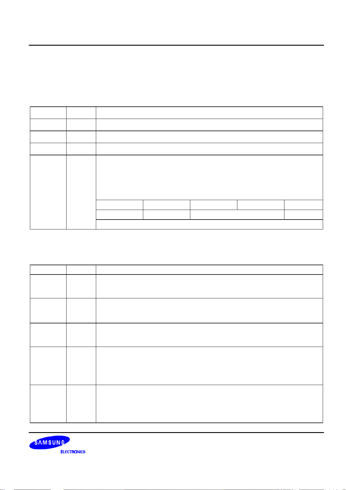
CGRAM has up to 5 x 8-dot 2 characters. By writing font data to CGRAM, user defined character can be used.
Table 6. Relationship between Character Code (DDRAM) and Character Pattern (CGRAM)
Character code
(DDRAM data)
CGRAM address CGRAM data
D7 D6 D5 D4 D3 D2 D1 D0 A3 A2 A1 A0 P7 P6 P5 P4 P3 P2 P1 P0
0 0 0 0 0 0 0 0
(00h)
0 0 0 0 0 0 0 1
(01h)
NOTE: "-" - Don’t care .
0 0 0 0
0 0 0 1
0 0 1 0
0 0 1 1
0 1 0 0
0 1 0 1
0 1 1 0
0 1 1 1
1 0 0 0
1 0 0 1
1 0 1 0
1 0 1 1
1 1 0 0
1 1 0 1
1 1 1 0
1 1 1 1
- - - 0 1 0 1 0
- - - 1 0 1 0 1
- - - 0 1 0 1 0
- - - 1 0 1 0 1
- - - 0 1 0 1 0
- - - 1 0 1 0 1
- - - 0 1 0 1 0
- - - 1 0 1 0 1
- - - 0 0 0 0 0
- - - 1 1 1 1 1
- - - 0 0 0 0 0
- - - 1 1 1 1 1
- - - 0 0 0 0 0
- - - 1 1 1 1 1
- - - 0 0 0 0 0
- - - 1 1 1 1 1
Pattern
number
Pattern 1
Pattern 2
12
Page 17

8 COM / 80 SEG DRIVER & CONTROLLER FOR STN LCD PRELIMINARY SPEC. VER. 0.5 S6A0031
LCD DRIVER CIRCUIT
LCD Driver circuit has 8 common and 80 segment signals for driving LCD. Data from CGRAM / CGROM are
transferred to 80-bit segment register serially, and then they are stored to 80-bit shift latch. COM1 to COM8 have 1/8
duty ratio. SEG bi-directional function is selected by DIRS input, and COM shift direction is selected by DIRC input.
Table 7. SEG Data Shift Direction
DIRS pin SEG data shift direction
Low
High
DIRC pin COM data shift direction
Low
High
SEG1 → SEG2 → SEG3 → - - - - - - - → SEG78 → SEG79 → SEG80
SEG80 → SEG79 → SEG78 → - - - - - - - → SEG3 → SEG2 → SEG1
Table 8. COM Data Shift Direction
COM1 → COM2 → COM3 → - - - - - - - - → COM6 → COM7 → COM8
COM8 → COM7 → COM6 → - - - - - - - - → COM3 → COM2 → COM1
13
Page 18

S6A0031 PRELIMINARY SPEC. VER. 0.5 8 COM / 80 SEG DRIVER & CONTROLLER FOR STN LCD
0 0 0 0 0 0 0 0 1
0 0 0 0 0 0 0 1 -
DDRAM address is set to 00h from AC and
Assign cursor moving direction and enable
Display ON / OFF
Set display (D), cursor (C), and blinking of
sor moving and display shift control
0 0 0 1 DL
internal operation or not can be
0 D7 D6 D5 D4 D3 D2 D1 D0
1 D7 D6 D5 D4 D3 D2 D1 D0
INSTRUCTION DESCRIPTION
Table 9. Instruction Table
Instruction RS R/W
*Clear display 0
DB7 DB6 DB5 DB4 DB3 DB2 DB1 DB0
Return home 0
Entry mode set
control
Cursor or display
shift
0 0 0 0 0 0 0 1 I/D SH
0 0 0 0 0 0 1 D C B
0 0 0 0 0 1 S/C R/L - -
Function set 0
CGRAM
address set
DDRAM
address set
Read busy flag
and address
0 0 0 1 0 0 A3 A2 A1 A0
0 0 1 0 0 A4 A3 A2 A1 A0
0 1 BF - - A4 A3 A2 A1 A0
- - - -
Description
Write "20H" to DDRAM and set DDRAM
address to "00H" from AC
the cursor returns to 00h position. The
contents of DDRAM are not changed.
the shift of entire display
cursor (B) ON / OFF control
Set cur
bit, and the direction, without changing of
DDRAM data
Set interface data length (DL: 4-bit / 8-bit)
instruction
Set CGRAM address in address counter.
Set DDRAM address in address counter.
Whether in
known by reading BF, The contents of
address counter can also be read
Write data 1
Read data 1
("-": Don’t care)
NOTES
1. Instruction execution time depends on the internal process time of S6A0031, therefore it is necessary to provide a time larger
than one MPU interface cycle time (tc) between execution of two successive instructions.
2. "Clear Display" instruction has 850µs execution time (when fosc = 40.0kHz), so check the Busy flag or wait for more than
850µs after using "Clear Display" instruction.
Write data into DDRAM / CGRAM
Read data from DDRAM / CGRAM
14
Page 19

8 COM / 80 SEG DRIVER & CONTROLLER FOR STN LCD PRELIMINARY SPEC. VER. 0.5 S6A0031
Clear Display
RS R/W DB7 DB6 DB5 DB4 DB3 DB2 DB1 DB0
0 0 0 0 0 0 0 0 0 1
Clear all the display data by writing "20H" (space code of CGROM) to all the DDRAM address, and set the DDRAM
address to "00H" into AC (address counter). For this instruction, the CGROM address "20H" have to set space code.
If the display position has shifted then it returns to the original positions. Namely, when display data is shifted and
cursor or blinking is displayed, bring the cursor to the left edge on first line of the display.
It makes entry mode to increment (I/D = "High").
Return Home
RS R/W DB7 DB6 DB5 DB4 DB3 DB2 DB1 DB0
0 0 0 0 0 0 0 0 1 -
Return Home instruction field makes cursor return home. DDRAM address is set to 00h from AC and the cursor
returns to 00h position. The contents of DDRAM are not changed.
Entry Mode Set
RS R/W DB7 DB6 DB5 DB4 DB3 DB2 DB1 DB0
0 0 0 0 0 0 0 1 I/D SH
Set the moving direction of cursor and display after data writing or reading instruction.
I/D: Increment / Decrement of DDRAM / CGRAM Address (Cursor or Blink)
After DDRAM / CGRAM data write/read operation, DDRAM / CGRAM address is increased (I/D = "High") or
decreased (I/D = "Low") by1. So in case of DDRAM data transfer operation and cursor or blink is turned on, cursor or
blink moves to right (I/D = "High") or left (I/D = "Low"), but in CGRAM data transfer operation, cursor or blink does not
move.
SH: Shift of Entire Display
When DDRAM read (CGRAM read / write) operation or SH = "Low", entire display is not shift. Only when SH =
"High" and DDRAM write operation, entire display is shift according to I/D value (I/D = "1": shift left, I/D = "0": shift
right).
Display ON / OFF Control
RS R/W DB7 DB6 DB5 DB4 DB3 DB2 DB1 DB0
0 0 0 0 0 0 1 D C B
Control display / cursor / blink ON / OFF 1 bit register.
D: Display ON / OFF Control Bit
When D = "High", entire display is turned ON.
When D = "Low", entire display is turned OFF, but display data is remained in DDRAM.
C: Cursor ON / OFF Control Bit
When C = "High", cursor is turned ON.
When C = "Low", cursor is disappeared in current display, but I/D register remains its data.
B: Cursor Blink ON / OFF Control Bit
When B = "High", cursor blink is ON, that performs alternate between all high data (black pattern) and display
character at the cursor position.
When B = "Low", blink is OFF.
15
Page 20

S6A0031 PRELIMINARY SPEC. VER. 0.5 8 COM / 80 SEG DRIVER & CONTROLLER FOR STN LCD
Cursor or Display Shift
RS R/W DB7 DB6 DB5 DB4 DB3 DB2 DB1 DB0
0 0 0 0 0 1 S/C R/L - -
Without writing or reading of display data, shift right/left the cursor position or display. This instruction is used to
correct or search display data (refer to table 10). Note that display shift is performed simultaneously in all the line.
When displayed data is shifted repeatedly, each line shifted individually. When display shift is performed, the
contents of address counter are not changed.
Table 10. Shift Patterns According to S/C and R/L Bits
S/C R/L Operation
0 0 Shift cursor to the left, AC is decreased by 1
0 1 Shift cursor to the right, AC is increased by 1
1 0 Shift all the display to the left, cursor moves according to the display
1 1 Shift all the display to the right, cursor moves according to the display
Function Set
RS R/W DB7 DB6 DB5 DB4 DB3 DB2 DB1 DB0
0 0 0 0 1 DL - - - -
DL: Interface Data Length Control Bit
When DL = "High", it means 8-bit bus mode with MPU.
When DL = "Low", it means 4-bit bus mode with MPU.
When 4-bit bus mode, it needs to transfer 4-bit data by two times.
CGRAM Address Set
RS R/W DB7 DB6 DB5 DB4 DB3 DB2 DB1 DB0
0 0 0 1 0 0 A3 A2 A1 A0
Set CGRAM address to AC
This instruction makes CGRAM data available from MPU for user defined character pattern. CGRAM address is
from 00h to 0Fh.
DDRAM Address Set
RS R/W DB7 DB6 DB5 DB4 DB3 DB2 DB1 DB0
0 0 1 0 0 A4 A3 A2 A1 A0
Set DDRAM address to AC
Before writing / reading data into / from the RAM, set the address by RAM Address Set instruction. Next, when data
are written/read in succession, the address is automatically increased by 1 (when I/D = "High") or decreased by 1
(when I/D = "Low"). The address ranges are 00h to 1Fh.
16
Page 21

8 COM / 80 SEG DRIVER & CONTROLLER FOR STN LCD PRELIMINARY SPEC. VER. 0.5 S6A0031
Read Busy Flag and Address
RS R/W DB7 DB6 DB5 DB4 DB3 DB2 DB1 DB0
0 1 BF - - A4 A3 A2 A1 A0
This instruction shows whether S6A0031 is in internal operation or not. If the resultant BF is "High", it means the
internal operation is in progress and you have to wait until BF to be "Low", and then the next instruction can be
performed. In this instruction you can read also the value of address counter.
Write Data
RS R/W DB7 DB6 DB5 DB4 DB3 DB2 DB1 DB0
1 0 D7 D6 D5 D4 D3 D2 D1 D0
Write binary 8- / 5- bit data to DDRAM / CGRAM
The selection of RAM from DDRAM / CGRAM is set by the previous address set instruction (DDRAM address set,
CGRAM address set). After write operation, the address is automatically increased / decreased by 1, according to
the entry mode.
Read Data
RS R/W DB7 DB6 DB5 DB4 DB3 DB2 DB1 DB0
1 1 D7 D6 D5 D4 D3 D2 D1 D0
Read binary 8- / 5- bit data from DDRAM / CGRAM
The selection of RAM is set by the previous address set instruction. If address set instruction of RAM is not
performed before this instruction, the data that read first is invalid, because the direction of AC is not determined. If
you read RAM data several times without RAM address set instruction before read operation, you can get correct
RAM data from the second, and the first data would be incorrect, because there is no time margin to transfer RAM
data. In case of DDRAM read operation, cursor shift instruction plays the same role as DDRAM address set
instruction: it also transfers RAM data to output data register.
After read operation address counter is automatically increased / decreased by 1 according to the entry mode. After
CGRAM read operation, display shift may not be executed correctly.
* In case of RAM write operation, after this operation, AC is increased / decreased by 1 like read operation. In this
time, AC indicates the next address position, but you can read only the previous data by read instruction. RAM
address is dummy data, so the correct RAM data come from the second read transaction. After reading operation,
the address is increased by 1 automatically.
17
Page 22

S6A0031 PRELIMINARY SPEC. VER. 0.5 8 COM / 80 SEG DRIVER & CONTROLLER FOR STN LCD
INITIALIZING
HARDWARE RESET
When the power is turned on, S6A0031 is initialized automatically by the power on reset circuit (refer to figure 8).
In case of RESETB pin becomes "Low" and durable the state for more than 1.2µs (VDD = 3V), S6A0031 can be
initialized too. During the initialization, the following instructions are executed, and BF (Busy Flag) is kept "High"
(busy state) to the end of initialization.
Display Clear
All the DDRAM data is set to "20H"
Return Home
Address counter = "00H"
Entry Mode Set Instruction
I/D = 1: Address counter is set to increment mode.
SH = 0: Entire display shift is disabled.
Display ON / OFF Control Instruction
C = 0: cursor OFF
B = 0: blink OFF
D = 0: display OFF
Function Set Instruction
DL = 1: 8-bit interface mode
CGRAM / DDRAM Address
RAM address counter is set to "00H".
t
RDD
VDD
0.1VDD
VDD Rising Time
Power Off Time
Note: If the upper power conditions are not satisfied in power on/off sequence, the internal
power on reset (POR) circuit will not operates normally.
t
OFF
0.9VDD
0.1VDD 0.1VDD
t
RDD
t
OFF
≤ 1 ms
≥ 1 ms
Figure 8. Power ON / OFF Timing
18
Page 23

8 COM / 80 SEG DRIVER & CONTROLLER FOR STN LCD PRELIMINARY SPEC. VER. 0.5 S6A0031
t
RW
t
R
RESETB
Internal Reset Time
Reset Pulse Width
Reset Time
Note: tRW indicates the minimum RESETB duration for activate internal reset signal
tR indicates reset completion time of internal circuit from the start of the internal
reset signal (when fosc = 40.0kHz).
t
RW
t
R
1.2 µs
850 µs
Figure 9. RESET Timing
19
Page 24

S6A0031 PRELIMINARY SPEC. VER. 0.5 8 COM / 80 SEG DRIVER & CONTROLLER FOR STN LCD
VDD-VSS Power ON
INSTRUCTION INITIALIZING WITH RESET
8-bit Interface Mode (fosc = 40.0kHz)
When Using RESETB
Input for Initializing
Wait until Power is Stable
Set Reset (RESETB Pin = "Low")
Wait for more than 1.2µs
Release Reset (RESETB Pin = "High")
Wait for more than 1ms
Command Input
Function Set
RS R/W DB7 DB6 DB5 DB4 DB3 DB2 DB1 DB0
0 0 0 0 1
Entry Mode Set
0 0 0 0 0 0 0 1 I/D SH
Display ON / OFF Control
0 0 0 0 0 0 1 D C B
DL
- - - -
(1)
When just Using Internal
Power On Reset Circuit
Wait for more than 20ms
after VDD rises to 0.9 VDD
End of Initialization
RAM Address Set
RAM Data Write
20
Page 25

8 COM / 80 SEG DRIVER & CONTROLLER FOR STN LCD PRELIMINARY SPEC. VER. 0.5 S6A0031
RAM Data Write
End of Initialization
RS
R/W
DB7
DB6
DB5
DB4
DB3
DB2
DB1
DB00000
1DL(0)
00000
0
0001I/D
SH
00000
0
001DC
B
VDD-VSS Power ON
Wait for more than 1ms
4-bit Interface Mode (fosc = 40.0kHz)
When Using RESETB
Input for Initializing
Wait until Power is Stable
Set Reset (RESETB Pin = "Low")
Wait for more than 1.2µs
Release Reset (RESETB Pin = "High")
Command Input
Function Set
- - - -
Entry Mode Set
- - - -
- - - -
Display ON / OFF Control
- - - -
- - - -
When just Using Internal
Power On Reset Circuit
Wait for more than 20ms
after VDD rises to 0.9 VDD
RAM Address Set
21
Page 26

S6A0031 PRELIMINARY SPEC. VER. 0.5 8 COM / 80 SEG DRIVER & CONTROLLER FOR STN LCD
GND
C1
V
LCD DRIVING POWER SUPPLY CIRCUIT
The Power Supply circuit produces LCD panel driving voltage at low power consumption. The LCD driving Power
Supply circuit consists of external voltage input and voltage follower.
DD
VDD
S6B0031
External
Power
Supply
O
P
E
N
* Recommended Capacitance value is 0.1 to 4.7µF
Figure 10. LCD Driving Power Connection
V0
V1
V2
V3
V4
VSS
22
Page 27

8 COM / 80 SEG DRIVER & CONTROLLER FOR STN LCD PRELIMINARY SPEC. VER. 0.5 S6A0031
GND
VCC
RESETB
GND
GND
VCC
RESETB
VCC
MPU INTERFACE
INTERFACING WITH 8080-SERIES MICROPROCESSORS
V
VCC
A0
A1 - A7
IORQ
MPU
(8080-series) RD
WR
D0 - D7
DECODER
RS
CSB MI
E_RD
RW_WR
DB0 - DB7
DD
S6A0031
RESET
GND
RESETB
V
Figure 11. Interfacing with 8080-series MPU
INTERFACING WITH 6800-SERIES MICROPROCESSORS
VCC
A0
A1 - A7
VMA
MPU
(6800 -series) E
R/W
D0 - D7
DECODER
RS
CSB MI
E_RD
RW_WR
DB0 - DB7
V
S6A0031
SS
DD
RESET
GND
RESETB
V
SS
Figure 12. Interfacing with 6800-series MPU
23
Page 28

S6A0031 PRELIMINARY SPEC. VER. 0.5 8 COM / 80 SEG DRIVER & CONTROLLER FOR STN LCD
SEG80
SEG79
SEG78
SEG1
SEG2
SEG3
•••••••••••••
APPLICATION INFORMATION FOR LCD PANEL
Chip Bottom & Lower View (DIRC = "0", DIRS = "0")
SEG77
COM8
COM7
COM6
•••
COM2
COM1
SEG1
SEG2
SEG3
SEG4
SEG5
SEG7
SEG6
SEG15
SEG14
SEG13
SEG12
SEG11
SEG10
SEG9
SEG8
BOTTOM VIEW
•••••••••••••
SEG76
Figure 13. Chip Bottom & Lower View Interfacing with LCD Panel
Chip Bottom & Upper View (DIRC = "1", DIRS = "1")
BOTTOM VIEW
SEG66
SEG67
SEG68
SEG69
SEG70
SEG71
SEG72
SEG73
SEG74
SEG75
SEG76
SEG77
SEG78
SEG79
SEG80
Figure 14. Chip Bottom & Upper View Interfacing with LCD Panel
SEG5
SEG4
COM1
COM2
•••
COM6
COM7
COM8
24
Page 29

8 COM / 80 SEG DRIVER & CONTROLLER FOR STN LCD PRELIMINARY SPEC. VER. 0.5 S6A0031
SEG1
SEG2
SEG3
SEG80
SEG79
SEG78
•••••••••••••
Chip Top & Lower View (DIRC = "0", DIRS = "1")
SEG4
SEG79
SEG80
SEG77
SEG78
SEG75
SEG76
SEG73
SEG74
SEG71
SEG72
SEG69
SEG70
SEG66
SEG67
SEG68
TOP VIEW
•••••••••••••
SEG5
COM8
COM7
COM6
COM2
COM1
•••
Figure 15. Chip Top & Lower View Interfacing with LCD Panel
Chip Top & Upper View (DIRC = "1", DIRS = "0")
COM1
COM2
•••
COM6
COM7
COM8
SEG1
SEG2
SEG3
SEG5
SEG4
SEG7
SEG6
SEG8
SEG9
SEG11
SEG10
TOP VIEW
SEG13
SEG12
Figure 16. Chip Top & Upper View Interfacing with LCD Panel
SEG15
SEG14
SEG77
SEG76
25
Page 30

S6A0031 PRELIMINARY SPEC. VER. 0.5 8 COM / 80 SEG DRIVER & CONTROLLER FOR STN LCD
VSSCOM1
FRAME FREQUENCY
1-line selection period
- - - -
21 87
87
- - - -
21 87
- - - -
21 87
- - - -
21
V0
V1
V4
1 FRAME
1-line Selection Period = 16 Clock Pulses x 4 Division
One Frame = 64 x 8 x 25.0µs = 12.8ms (1 Clock = 25.0µs at fosc = 40.0kHz)
Frame Frequency
= 1 / 12.8ms = 78Hz
1 FRAME
Figure 17. Frame Frequency
26
Page 31

8 COM / 80 SEG DRIVER & CONTROLLER FOR STN LCD PRELIMINARY SPEC. VER. 0.5 S6A0031
MAXIMUM ABSOLUTE RATE
Table 11. Maximum Absolute Rate
Characteristics Symbol Value Unit
Power supply voltage (1) VDD -0.3 to +7.0 V
Power supply voltage (2) V0 -0.3 to + 8.0 V
Input voltage VIN -0.3 to VDD +0.3 V
Operating temperature T
Storage temperature T
NOTE: 1. All the voltage levels are based on VSS = 0V.
2. Voltage greater than above may damage the circuit.
Voltage level: V0 ≥ VDD ≥ VSS
Voltage level: V0 ≥ V1 ≥ V2 = V3 ≥ V4 ≥ VSS
-30 to +85
OPR
-55 to +125
STG
°C
°C
27
Page 32

S6A0031 PRELIMINARY SPEC. VER. 0.5 8 COM / 80 SEG DRIVER & CONTROLLER FOR STN LCD
ELECTRICAL CHARACTERISTICS
DC CHARACTERISTICS
Table 12. DC Characteristics
(VDD = 2.4V to 3.6V, Ta = -30 to +85 oC)
Item Symbol
Operating voltage VDD - 2.4 - 3.6 V
I
Supply current
DD1
(VDD = 3V, Ta = 25 oC)
I
DD2
Access operation from MPU
Condition Min. Typ. Max. Unit
Display operation
V0 = 6V without load
- - 50
No access from MPU
fcyc = 200kHz
- - 500
µA
Input voltage
Input leakage current I
RON resistance
Frame frequency fFR VDD = 3V, Ta = 25 oC 55 78 101 Hz
External clock
frequency
LCD driving voltage V
VIH - 0.7VDD
- VDD
V
VIL - VSS - 0.3VDD
V
LEAK
R
COM
= 0V to VDD -1 - 1
IN
Io = ± 50µA
- - 5
µA
kΩ
R
SEG
Io = ± 50µA
- - 10
fCK - - 40.0 - kHz
V
LCD
= V0 – VSS 3.0 - 6.0 V
LCD
28
Page 33

8 COM / 80 SEG DRIVER & CONTROLLER FOR STN LCD PRELIMINARY SPEC. VER. 0.5 S6A0031
frequency
Table 12. DC Characteristics (Continued)
(VDD = 3.6V to 5.5V, Ta = -30 to +85 oC)
Item Symbol
Condition Min. Typ. Max. Unit
Operating voltage VDD - 3.6 - 5.5 V
Display operation
I
Supply current
(VDD = 5V, Ta = 25 oC)
DD1
I
DD2
V0 = 6V without load
No access from MPU
Access operation from MPU
fcyc = 200kHz
- - 80
µA
- - 1000
VIH - 0.7VDD
- VDD
Input voltage
VIL - VSS - 0.3VDD
Input leakage current I
V
LEAK
R
COM
= 0V to VDD -1 - 1
IN
Io = ± 50µA
- - 5
RON resistance
R
SEG
Io = ± 50µA
- - 10
Frame frequency fFR VDD = 3V, Ta = 25 oC 55 78 101 Hz
External clock
LCD driving voltage V
fCK - - 40.0 - kHz
V
LCD
= V0 – VSS 3.6 - 6.0 V
LCD
V
µA
kΩ
29
Page 34

S6A0031 PRELIMINARY SPEC. VER. 0.5 8 COM / 80 SEG DRIVER & CONTROLLER FOR STN LCD
tCtH2t
SU2tRtFtWLtWHtH1tSU1
AC CHARACTERISTICS
6800-Series MPU Interface & Write Instruction
Table 13. AC Characteristics (6800-series Write Instruction)
Condition Characteristic
E cycle time tC 650 -
Pulse rise / fall time tR, tF - - 25
E pulse width high tWH 450 - -
VDD = 2.4V to 3.6V,
E pulse width low tWL 150 - -
Ta = -30 to +85 oC
RS and CSB setup time t
RS and CSB hold time tH1 30 - -
DB setup time t
DB hold time tH2 50 - -
E cycle time tC 350 -
Pulse rise / fall time tR, tF - - 25
E pulse width high tWH 250 - -
VDD = 3.6V to 5.5V,
Ta = -30 to +85 oC
E pulse width low tWL 100 - -
RS and CSB setup time t
RS and CSB hold time tH1 10 - -
DB setup time t
DB hold time tH2 10 - -
Symbol
SU1
SU2
SU1
SU2
Min. Typ. Max. Unit
60 - -
100 - -
40 - -
40 - -
ns
ns
RS, CSB
RW_WR
E_RD
DB0 to DB7
Figure 18. Write Bus Mode Timing (6800-series MPU Interface)
30
Page 35

8 COM / 80 SEG DRIVER & CONTROLLER FOR STN LCD PRELIMINARY SPEC. VER. 0.5 S6A0031
t
R
t
C
tH2t
SU2
t
F
t
WH
tWLtH1t
SU1
8080-series MPU Interface & Write Instruction
Table 14. AC Characteristics (8080-series Write Instruction)
Condition Characteristic
WR cycle time tC 650 -
Pulse rise / fall time tR, tF - - 25
WR pulse width high tWH 150 - -
VDD = 2.4V to 3.6V,
Ta = -30 to +85 oC
WR pulse width low tWL 450 - -
RS and CSB setup time t
RS and CSB hold time tH1 30 - -
DB setup time t
DB hold time tH2 50 - -
WR cycle time tC 350 -
Pulse rise / fall time tR, tF - - 25
WR pulse width high tWH 100 - -
VDD = 3.6V to 5.5V,
Ta = -30 to +85 oC
WR pulse width low tWL 250 - -
RS and CSB setup time t
RS and CSB hold time tH1 10 - -
DB setup time t
DB hold time tH2 10 - -
Symbol
SU1
SU2
SU1
SU2
Min. Typ. Max. Unit
60 - -
100 - -
40 - -
40 - -
ns
ns
RS, CSB
RW_WR
DB0 to DB7
Figure 19. Write Bus Mode Timing (8080-series MPU Interface)
31
Page 36

S6A0031 PRELIMINARY SPEC. VER. 0.5 8 COM / 80 SEG DRIVER & CONTROLLER FOR STN LCD
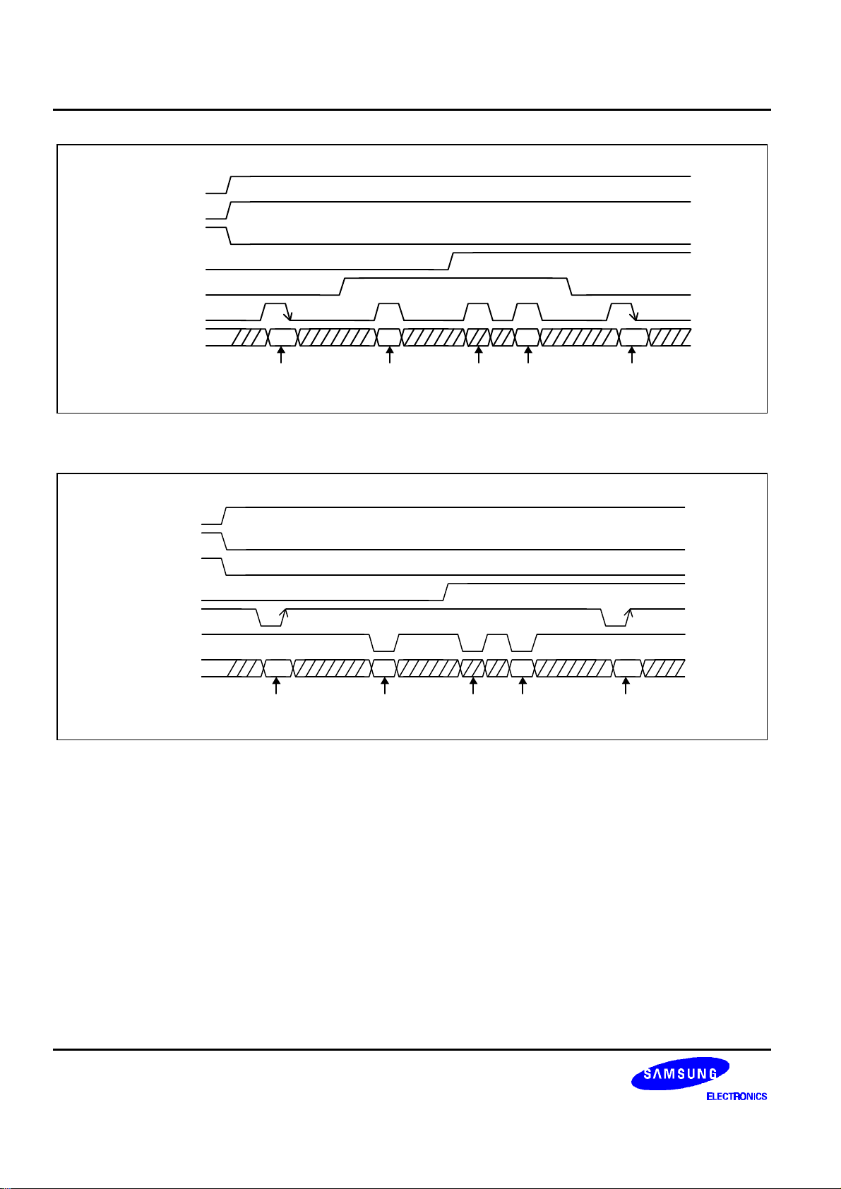
tSUtCtDHtDtFtRtHtWLt
WH
6800-series MPU Interface & Read Instruction
Table 15. AC Characteristics (6800-series Read Instruction)
Condition Characteristic
VDD = 2.4V to 3.6V,
Ta = -30 to +85 oC
VDD = 3.6V to 5.5V,
Ta = -30 to +85 oC
Symbol
Min. Typ. Max. Unit
E cycle time tC 650 -
Pulse rise / fall time tR, tF - - 25
E pulse width high tWH 450 - -
E pulse width low tWL 150 - -
RS and CSB setup time tSU 60 - -
RS and CSB hold time tH 30 - -
DB output delay time tD - - 360
DB output hold time tDH 20 - -
E cycle time tC 350 -
Pulse rise / fall time tR, tF - - 25
E pulse width high tWH 250 - -
E pulse width low tWL 100 - -
RS and CSB setup time tSU 40 - -
RS and CSB hold time tH 10 - -
DB output delay time tD - - 120
DB output hold time tDH 10 - -
ns
ns
RS, CSB
RW_WR
E_RD
DB0 to DB7
Figure 20. Read Bus Mode Timing (6800-series MPU Interface)
32
Page 37

8 COM / 80 SEG DRIVER & CONTROLLER FOR STN LCD PRELIMINARY SPEC. VER. 0.5 S6A0031
t
R
t
C
tDHt
D
tFtWHtWLtHt
SU
8080-series MPU Interface & Read Instruction
Table 16. AC Characteristics (8080-series read instruction)
Condition Characteristic
RD cycle time tC 650 Pulse rise / fall time tR, tF - - 25
RD pulse width high tWH 150 - -
VDD = 2.4V to 3.6V,
Ta = -30 to +85 oC
RD pulse width low tWL 450 - -
RS and CSB setup time tSU 60 - -
RS and CSB hold time tH 30 - -
DB output delay time tD - 360
DB output hold time tDH 20 - -
RD cycle time tC 350 Pulse rise / fall time tR, tF - - 25
RD pulse width high tWH 100 - -
VDD = 3.6V to 5.5V,
Ta = -30 to +85 oC
RD pulse width low tWL 250 - -
RS and CSB setup time tSU 40 - -
RS and CSB hold time tH 10 - -
DB output delay time tD - - 120
DB output hold time tDH 10 - -
Symbol
Min. Typ. Max. Unit
ns
ns
RS, CSB
E_RD
DB0 to DB7
Figure 21. Read Bus Mode Timing (8080-series MPU Interface)
33
 Loading...