

Page 1
NTF5P03T3
l
s
l
Preferred Device
Power MOSFET
5.2 Amps, 30 Volts
P−Channel SOT−223
Features
• Ultra Low R
DS(on)
• Higher Efficiency Extending Battery Life
• Logic Level Gate Drive
• Miniature SOT−223 Surface Mount Package
• Avalanche Energy Specified
• Pb−Free Package is Available
Applications
• DC−DC Converters
• Power Management
• Motor Controls
• Inductive Loads
• Replaces MMFT5P03HD
http://onsemi.com
5.2 AMPERES, 30 VOLTS
= 100 mW
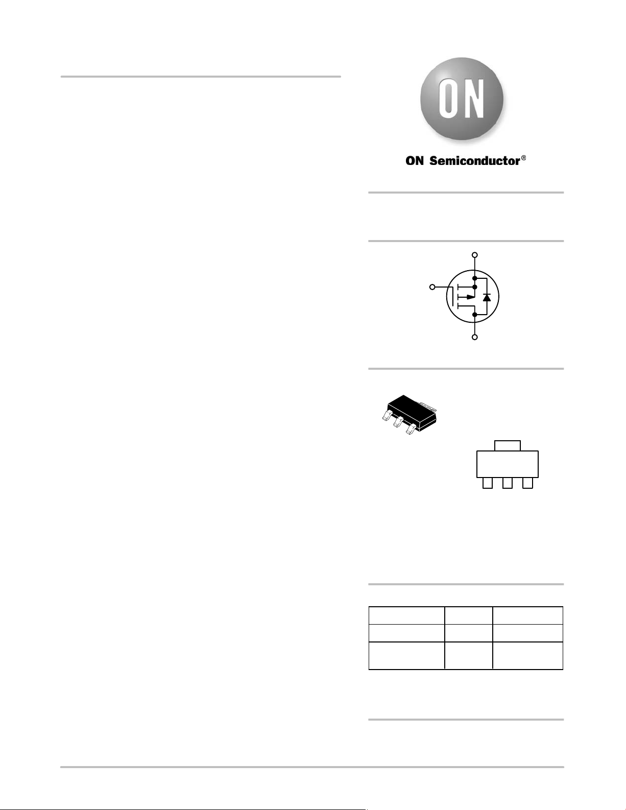
S
D
P−Channel MOSFET
MARKING
4
DIAGRAM
& PIN
ASSIGNMENT
Drain
AYM
5P03 G
1
2
SOT−223
CASE 318E
STYLE 3
3
R
DS(on)
G
4
G
© Semiconductor Components Industries, LLC, 2006
December, 2006 − Rev. 3
1
Gate2Drain3Source
A = Assembly Location
Y = Year
M = Date Code
5P03 = Specific Device Code
G = Pb−Free Package
(Note: Microdot may be in either location)
ORDERING INFORMATION
Device Package Shipping
NTF5P03T3 SOT−223 4000/Tape & Ree
NTF5P03T3G
†For information on tape and reel specifications,
including part orientation and tape sizes, please
refer to our Tape and Reel Packaging Specification
Brochure, BRD801 1/D.
Preferred devices are recommended choices for future use
and best overall value.
1
SOT−223
(Pb−Free)
Publication Order Number:
4000/Tape & Ree
NTF5P03T3/D
†
Page 2

NTF5P03T3
MAXIMUM RATINGS (T
= 25°C unless otherwise noted)
J
Negative sign for P−Channel devices omitted for clarity
Rating
Drain−to−Source Voltage V
Drain−to−Gate Voltage (RGS = 1.0 MW)
Gate−to−Source Voltage − Continuous V
1 sq in
FR−4 or G−10 PCB
10 seconds
Thermal Resistance − Junction to Ambient
Total Power Dissipation @ T
Linear Derating Factor
Drain Current − Continuous @ T
Continuous @ TA = 70°C
= 25°C
A
A
= 25°C
Pulsed Drain Current (Note 1)
Minimum
FR−4 or G−10 PCB
Thermal Resistance − Junction to Ambient
Total Power Dissipation @ T
= 25°C
A
Linear Derating Factor
10 seconds
Drain Current − Continuous @ T
Continuous @ T
= 70°C
A
= 25°C
A
Pulsed Drain Current (Note 1)
Operating and Storage Temperature Range TJ, T
Single Pulse Drain−to−Source Avalanche Energy − Starting TJ = 25°C
(V
= −30 Vdc, VGS = −10 Vdc, Peak IL = −12 Apk, L = 3.5 mH, RG = 25 W)
DD
Symbol Max Unit
−30 V
−30 V
± 20 V
40
3.13
25
°C/W
Watts
mW/°C
−5.2
−4.1
−26
80
1.56
12.5
°C/W
Watts
mW/°C
−3.7
−2.9
−19
− 55 to 150 °C
mJ
250
A
A
A
A
A
A
V
R
R
DSS
DGR
GS
THJA
P
I
D
I
D
I
DM
THJA
P
I
D
I
D
I
DM
E
AS
D
D
stg
Stresses exceeding Maximum Ratings may damage the device. Maximum Ratings are stress ratings only. Functional operation above the
Recommended Opera t i n g Conditions is not implied. Extended exposure to stresses above the Recommended Operating Conditions may affect
device reliability.
1. Repetitive rating; pulse width limited by maximum junction temperature.
http://onsemi.com
2
Page 3
NTF5P03T3
ELECTRICAL CHARACTERISTICS (T
= 25°C unless otherwise noted)
A
Characteristic
OFF CHARACTERISTICS
Drain−to−Source Breakdown Voltage (Cpk ≥ 2.0) (Notes 2 and 4)
(V
= 0 Vdc, ID = −0.25 mAdc)
GS
Temperature Coefficient (Positive)
Zero Gate Voltage Drain Current
(VDS = −24 Vdc, VGS = 0 Vdc)
(VDS = −24 Vdc, VGS = 0 Vdc, TJ = 125°C)
Gate−Body Leakage Current
(V
= ± 20 Vdc, VDS = 0 Vdc)
GS
ON CHARACTERISTICS (Note 2)
Gate Threshold Voltage
(VDS = VGS, ID = −0.25 mAdc)
Threshold Temperature Coefficient (Negative)
Static Drain−to−Source On−Resistance (Cpk ≥ 2.0) (Notes 2 and 4)
(V
= −10 Vdc, ID = −5.2 Adc)
GS
(VGS = −4.5 Vdc, ID = −2.6Adc)
Forward Transconductance (Note 2)
(V
= −15 Vdc, ID = −2.0 Adc)
DS
(Cpk ≥ 2.0) (Notes 2 and 4)
DYNAMIC CHARACTERISTICS
Input Capacitance
Output Capacitance C
(VDS = −25 Vdc, V
f = 1.0 MHz)
Transfer Capacitance C
GS
= 0 V,
SWITCHING CHARACTERISTICS (Note 3)
(V
Turn−On Delay Time
Rise Time t
= −15 Vdc, ID = −4.0 Adc,
DD
V
= −10 Vdc,
GS
= 6.0 W) (Note 2)
R
G
Turn−Off Delay Time t
Fall Time t
(V
Turn−On Delay Time
Rise Time t
= −15 Vdc, ID = −2.0 Adc,
DD
V
= −10 Vdc,
GS
= 6.0 W) (Note 2)
R
G
Turn−Off Delay Time t
Fall Time t
Gate Charge (VDS = −24 Vdc, ID = −4.0 Adc,
V
= −10 Vdc) (Note 2)
GS
SOURCE−DRAIN DIODE CHARACTERISTICS
Forward On−Voltage (IS = −4.0 Adc, VGS = 0 Vdc)
Reverse Recovery Time (IS = −4.0 Adc, VGS = 0 Vdc,
Reverse Recovery Stored Charge Q
2. Pulse Test: Pulse Width ≤ 300 ms, Duty Cycle ≤ 2.0%.
3. Switching characteristics are independent of operating junction temperatures.
4. Reflects typical values.
Cpk +
Ť
(I
= −4.0 Adc, VGS = 0 Vdc,
S
TJ = 125°C) (Note 2)
dIS/dt = 100 A/ms) (Note 2)
Max limit * Typ
3 SIGMA
Ť
Symbol Min Typ Max Unit
V
(BR)DSS
I
DSS
I
GSS
V
GS(th)
R
DS(on)
g
C
t
d(on)
d(off)
t
d(on)
d(off)
Q
Q
Q
fs
iss
oss
rss
r
f
r
f
−30
−
−
−
−
−28
−
−
−
−
−1.0
−25
− − ± 100 nAdc
−1.0
−
− 76
−1.75
3.5
107
−3.0
−
100
150
2.0 3.9 − Mhos
− 500 950
− 153 440
− 58 140
− 10 24
− 33 48
− 38 94
− 20 92
− 16 38
− 45 110
− 23 60
− 24 80
T
1
2
− 15 38
− 1.6 −
− 3.5 −
Vdc
mV/°C
mAdc
Vdc
mV/°C
mW
pF
ns
ns
nC
Q3 − 2.6 −
V
t
t
t
SD
rr
a
b
RR
−
−
−1.1
−0.89
−1.5
− 34 −
− 20 −
− 14 −
− 0.036 −
−
Vdc
ns
mC
http://onsemi.com
3
Page 4

10
0
−I
DRAIN CURRENT (AMPS)
5
4
VGS = −8.0 V
3
VGS = −10 V
TJ = 25°C
2
D,
1
0
0
0.100
0.075
NTF5P03T3
TYPICAL ELECTRICAL CHARACTERISTICS
VGS = −4.3 V
VGS = −4.5 V
VGS = −6.0 V
VGS = −4.1 V
VGS = −3.9 V
8
6
VGS = −3.7 V
4
VGS = −3.5 V
0.9
−V
DRAIN−TO−SOURCE VOLTAGE (VOLTS)
DS,
1.20.60.3
VGS = −3.3 V
VGS = −3.1 V
VGS = −2.7 V
1.5 1.8
DRAIN CURRENT (AMPS)
2
D,
−I
0
Figure 1. On−Region Characteristics Figure 2. Transfer Characteristics
0.20
ID = −4.0 A
T
= 25°C
J
0.15
V
≥ −10 V
DS
TJ = 25°C
TJ = 100°C
TJ = −55°C
363.5 54 4.5 5.5
−V
GATE−TO−SOURCE VOLTAGE (VOLTS)
GS,
TJ = 25°C
VGS = −4.5 V
0.050
0.025
DRAIN−TO−SOURCE RESISTANCE (W)
0
DS(on),
R
0
13
GATE−TO−SOURCE VOLTAGE (VOLTS)
−V
GS,
Figure 3. On−Resistance versus
Gate−to−Source V oltage
1.6
ID = −2.0 A
V
= −10 V
GS
1.4
1.2
1
(NORMALIZED)
0.8
DRAIN−TO−SOURCE RESISTANCE
0.6
−50 50250−25 75 125100
DS(on),
R
T
, JUNCTION TEMPERATURE (°C)
J
Figure 5. On−Resistance Variation with
Temperature
0.10
VGS = −10 V
0.05
DRAIN−TO−SOURCE RESISTANCE (W)
DS(on),
R
0
0
1
4653
−ID, DRAIN CURRENT (AMPS)
42
52
Figure 4. On−Resistance versus Drain Current
and Gate Voltage
100
VGS = 0 V
TJ = 125°C
10
, LEAKAGE (nA)
150
DSS
−I
1
0253
−V
DRAIN−TO−SOURCE VOLTAGE (VOLTS)
DS,
TJ = 100°C
2010 15
Figure 6. Drain−to−Source Leakage Current
versus Voltage
78
http://onsemi.com
4
Page 5

NTF5P03T3
C, CAPACITANCE (pF)
t, TIME (ns)
−I
, DRAIN CURRENT (AMPS)
0
0
DS
TYPICAL ELECTRICAL CHARACTERISTICS
6000
5000
VDS = 0 V
C
iss
VGS = 0 V
TJ = 25°C
12.5
10
−V
DS
4000
C
rss
7.5
3000
C
iss
2000
C
oss
1000
C
rss
0
−V
10 1002030
GS
−V
DS
5.0
Q
1
2.5
, GATE−TO−SOURCE VOLTAGE (V)
GS
0
−V
0504020 60
GATE−TO−SOURCE OR DRAIN−TO−SOURCE VOLTAGE
(VOLTS)
Figure 7. Capacitance Variation Figure 8. Gate−to−Source and
Drain−to−Source V oltage versus Total Charge
1000
100
VDD = −15 V
I
= −4.0 A
D
= −10 V
V
GS
t
d(off)
t
f
t
r
3
2
1
VGS = 0 V
T
J
= 25°C
Q
T
Q
2
3010
Q
, TOTAL GATE CHARGE (nC)
g
−V
GS
ID = −2 A
T
= 25°C
J
25
20
15
10
5
0
, DRAIN−TO−SOURCE VOLTAGE (V)
−V
10
1 10 100 0.5 0.70.6 1.
100
10
1
0.1
D
0.01
0.1 10 1001 25 125 15
Mounted on 2”sq. FR4 board (1”sq. 2 oz. Cu 0.06” thick
single sided) with on die operating, 10 s max.
t
d(on)
RG, GATE RESISTANCE (W)
Figure 9. Resistive Switching Time Variation
versus Gate Resistance
VGS = 20 V
SINGLE PULSE
TC = 25°C
dc
10 ms
1 ms
100 ms
R
LIMIT
DS(on)
10 ms
THERMAL LIMIT
PACKAGE LIMIT
−VDS, DRAIN−TO−SOURCE VOLTAGE (VOLTS)
Figure 11. Maximum Rated Forward Biased
Safe Operating Area
, SOURCE CURRENT (AMPS)
S
−I
0
0.8 0.9
−VSD, SOURCE−TO−DRAIN VOLTAGE (VOLTS)
Figure 10. Diode Forward Voltage versus Current
350
300
250
200
150
100
AVALANCHE ENERGY (mJ)
50
, SINGLE PULSE DRAIN−TO−SOURCE
AS
0
E
1007550
TJ, STARTING JUNCTION TEMPERATURE (°C)
Figure 12. Maximum Avalanche Energy versus
Starting Junction Temperature
ID = −6 A
http://onsemi.com
5
Page 6

NTF5P03T3
TYPICAL ELECTRICAL CHARACTERISTICS
1
D = 0.5
0.2
0.1
0.05
0.1
0.02
, EFFECTIVE TRANSIENT
THERMAL RESPONSE
THJA(t)
R
SINGLE PULSE
0.01
1.0E−03 1.0E−02 1.0E−01 1.0E+00 1.0E+01
0.01
CHIP
JUNCTION
Figure 13. FET Thermal Response
NORMALIZED TO R
0.0175 W
0.0154 F
t, TIME (s)
0.0710 W
0.0854 F
AT STEADY STATE (1″ PAD)
q
JA
0.2706 W
0.3074 F
0.5779 W
1.7891 F
0.7086 W
107.55 F
1.0E+02 1.0E+03
AMBIENT
http://onsemi.com
6
Page 7

b1
NTF5P03T3
PACKAGE DIMENSIONS
SOT−223 (TO−261)
CASE 318E−04
D
ISSUE L
NOTES:
1. DIMENSIONING AND TOLERANCING PER ANSI
Y14.5M, 1982.
2. CONTROLLING DIMENSION: INCH.
0.08 (0003)
H
e1
E
A1
4
123
e
E
b
q
A
SOLDERING FOOTPRINT*
2.0
0.079
2.3
0.091
3.8
0.15
L1
C
2.3
0.091
DIMAMIN NOM MAX MIN
A1 0.02 0.06 0.10 0.001
b 0.60 0.75 0.89 0.024
b1 2.90 3.06 3.20 0.115
c 0.24 0.29 0.35 0.009
D 6.30 6.50 6.70 0.249
E 3.30 3.50 3.70 0.130
e 2.20 2.30 2.40 0.087
e1
L1 1.50 1.75 2.00 0.060
H
E
q
STYLE 3:
PIN 1. GATE
MILLIMETERS
1.50 1.63 1.75 0.060
0.85 0.94 1.05 0.033
6.70 7.00 7.30 0.264
0° 10° 0° 10°
− −
2. DRAIN
3. SOURCE
4. DRAIN
6.3
0.248
INCHES
NOM MAX
0.064 0.068
0.002 0.004
0.030 0.035
0.121 0.126
0.012 0.014
0.256 0.263
0.138 0.145
0.091 0.094
0.037 0.041
0.069 0.078
0.276 0.287
2.0
0.079
1.5
0.059
SCALE 6:1
ǒ
inches
mm
Ǔ
*For additional information on our Pb−Free strategy and
soldering details, please download the ON Semiconductor
Soldering and Mounting Techniques Reference Manual,
SOLDERRM/D.
ON Semiconductor and are registered trademarks of Semiconductor Components Industries, LLC (SCILLC). SCILLC reserves the right to make changes without further notice
to any products herein. SCILLC makes no warranty, representation or guarantee regarding the suitability of its products for any particular purpose, nor does SCILLC assume any liability
arising out of the application or use of any product or circuit, and specifically disclaims any and all liability, including without limitation special, consequential or incidental damages.
“Typical” parameters which may be provided in SCILLC data sheets and/or specifications can and do vary in different applications and actual performance may vary over time. All
operating parameters, including “Typicals” must be validated for each customer application by customer’s technical experts. SCILLC does not convey any license under its patent rights
nor the rights of others. SCILLC products are not designed, intended, or authorized for use as components in systems intended for surgical implant into the body, or other applications
intended to support or sustain life, or for any other application in which the failure of the SCILLC product could create a situation where personal injury or death may occur. Should
Buyer purchase or use SCILLC products for any such unintended or unauthorized application, Buyer shall indemnify and hold SCILLC and its officers, employees, subsidiaries, affiliates,
and distributors harmless against all claims, costs, damages, and expenses, and reasonable attorney fees arising out of, directly or indirectly, any claim of personal injury or death
associated with such unintended or unauthorized use, even if such claim alleges that SCILLC was negligent regarding the design or manufacture of the part. SCILLC is an Equal
Opportunity/Affirmative Action Employer. This literature is subject to all applicable copyright laws and is not for resale in any manner.
PUBLICATION ORDERING INFORMATION
LITERATURE FULFILLMENT:
Literature Distribution Center for ON Semiconductor
P.O. Box 5163, Denver, Colorado 80217 USA
Phone: 303−675−2175 or 800−344−3860 Toll Free USA/Canada
Fax: 303−675−2176 or 800−344−3867 Toll Free USA/Canada
Email: orderlit@onsemi.com
N. American Technical Support: 800−282−9855 Toll Free
USA/Canada
Europe, Middle East and Africa Technical Support:
Phone: 421 33 790 2910
Japan Customer Focus Center
Phone: 81−3−5773−3850
http://onsemi.com
ON Semiconductor Website: www.onsemi.com
Order Literature: http://www.onsemi.com/orderlit
For additional information, please contact your local
Sales Representative
NTF5P03T3/D
7
 Loading...