

Page 1

NTE944 & NTE944M
Integrated Circuit
Programmable Operational Amplifier
Description:
The NTE944 (8–Lead Metal Can) and NTE944M (8–Lead MiniDIP) are extremely versatile program mable monolithic o perational amplifiers. A s ingle external master b ias current setting r esistor programs
the input b ias c urrent, i nput o ffset c urrent, quiescent power c onsumption, s lew r ate, i nput n oise, a nd t he
gain–bandwidth product. These devices are truly general purpose operational amplifiers.
Features:
D ±1V to ±18V power supply operation
D 3nA input offset current
D Standby power consumption as low as 500mW
D No frequency compensation required
D Programmable electrical characteristics
D Offset voltage nulling capability
D Can be powered by two flashlight batteries
D Short circuit protection
Absolute Maximum Ratings:
Supply Voltage ±18V. . . . . . . . . . . . . . . . . . . . . . . . . . . . . . . . . . . . . . . . . . . . . . . . . . . . . . . . . . . . . . . . . . . .
Power Dissipation (Note 1) 500mW. . . . . . . . . . . . . . . . . . . . . . . . . . . . . . . . . . . . . . . . . . . . . . . . . . . . . .
Differential Input Voltage ±30V. . . . . . . . . . . . . . . . . . . . . . . . . . . . . . . . . . . . . . . . . . . . . . . . . . . . . . . . . . .
Input Voltage (Note 2) ±15V. . . . . . . . . . . . . . . . . . . . . . . . . . . . . . . . . . . . . . . . . . . . . . . . . . . . . . . . . . . . . .
I
Current 150µA. . . . . . . . . . . . . . . . . . . . . . . . . . . . . . . . . . . . . . . . . . . . . . . . . . . . . . . . . . . . . . . . . . . . .
SET
Output Short Circuit Duration Indefinite. . . . . . . . . . . . . . . . . . . . . . . . . . . . . . . . . . . . . . . . . . . . . . . . . . .
Operating Temperature Range 0° ≤ T
Storage Temperature Range –65° to +150°C. . . . . . . . . . . . . . . . . . . . . . . . . . . . . . . . . . . . . . . . . . . . . . .
Lead Temperature (Soldering, 10sec) +300°C. . . . . . . . . . . . . . . . . . . . . . . . . . . . . . . . . . . . . . . . . . . . . .
Note 1. The maximum junction temperature of the NTE944 is 100°C. F or o perating a t elevated tem-
peratures, the NTE944 must be derated based on a thermal resistance of 150°C/W junction
to ambient, o r 45°C/W j unction t o c ase. T he t hermal r esistance o f t he N TE944M i s + 125°C/W.
Note 2. For s upply v oltages l ess t han ±15V , t he a bsolute m aximum i nput v oltage i s e qual t o t he s upply
voltage.
≤ +70°C. . . . . . . . . . . . . . . . . . . . . . . . . . . . . . . . . . . . . . . . . . . .
A
Page 2
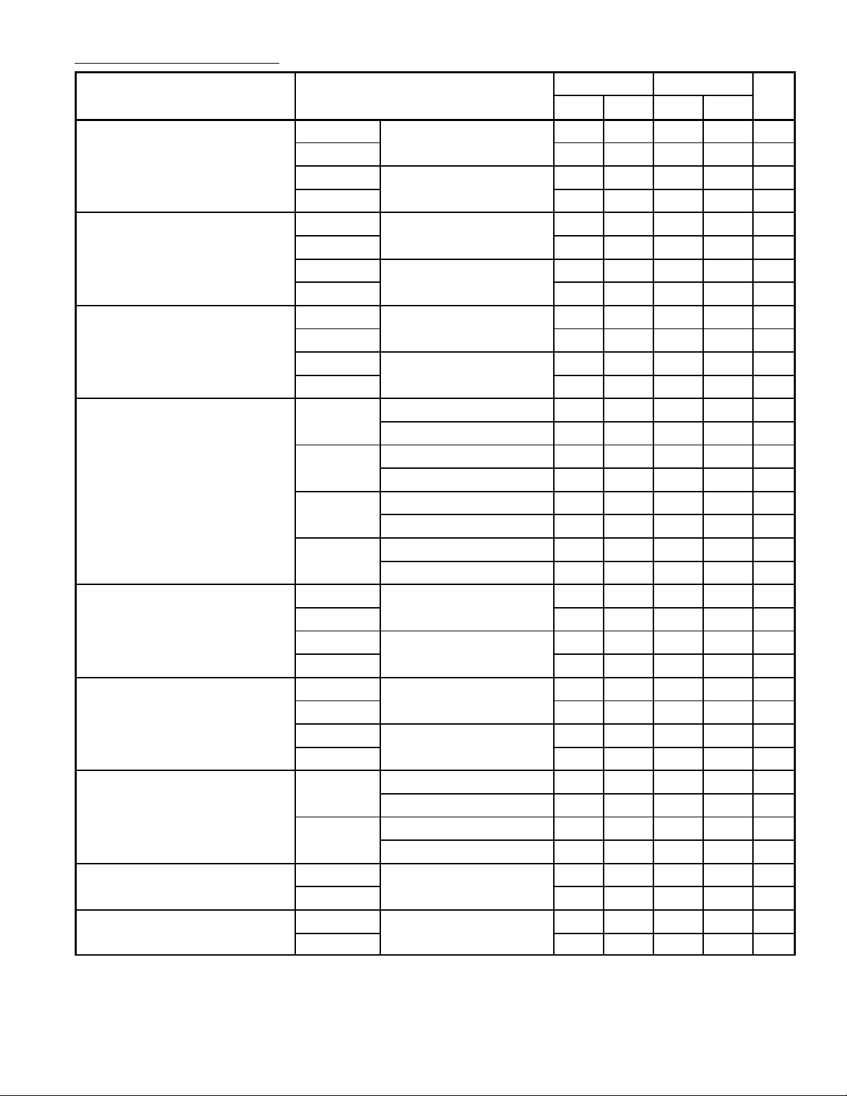
Electrical Characteristics: (0° ≤ TA ≤+70°C, unless otherwise specified)
I
= 1µA I
Parameter Test Conditions
SET
Min Max Min Max
SET
= 10µA
Unit
V
OS
VS = ±1.5V TA = +25°C, RS ≤ 100kΩ – 5 – 6 mV
VS = ±15V – 5 – 6 mV
VS = ±1.5V RS ≤ 10kΩ – 6.5 – 7.5 mV
VS = ±15V – 6.5 – 7.5 mV
I
OS
VS = ±1.5V TA = +25°C – 6 – 20 nA
VS = ±15V – 6 – 20 nA
VS = ±1.5V – 8 – 25 nA
VS = ±15V – 8 – 25 nA
I
bias
VS = ±1.5V TA = +25°C – 10 – 75 nA
VS = ±15V – 10 – 75 nA
VS = ±1.5V – 10 – 80 nA
VS = ±15V – 10 – 80 nA
Large Signal Voltage Gain VS = ±1.5V TA = +25°C, RL ≤ 100kΩ 25k – – –
VO = ±0.6V, RL ≤ 10kΩ – – 25k –
VS = ±15V TA = +25°C, RL ≤ 100kΩ 60k – – –
VO = ±10V, RL ≤ 10kΩ – – 60k –
VS = ±1.5V VO = ±0.5V, RL = 100kΩ 25k – – –
RL = 10kΩ – – 25k –
VS = ±15V VO = ±10V, RL = 100kΩ 50k – – –
RL = 10kΩ – – 50k –
Supply Current VS = ±1.5V TA = +25°C – 8 – 90 µA
VS = ±15V – 11 – 100 µA
VS = ±1.5V – 8 – 90 µA
VS = ±15V – 11 – 100 µA
Power Consumption VS = ±1.5V TA = +25°C – 24 – 270 µW
VS = ±15V – 330 – 3k µW
VS = ±1.5V – 24 – 270 µW
VS = ±15V – 330 – 3k µW
Output Voltage Swing VS = ±1.5V RL = 100kΩ ±0.6 – – – V
RL = 10kΩ – – ±0.6 – V
VS = ±15V RL = 100kΩ ±12 – – – V
RL = 10kΩ – – ±12 – V
Common Mode Rejection Ratio VS = ±1.5V RS ≤ 10kΩ 70 – 70 – dB
VS = ±15V 70 – 70 – dB
Supply Voltage Rejection Ratio VS = ±1.5V RS ≤ 10kΩ 74 – 74 – dB
VS = ±15V 74 – 74 – dB
Page 3

Resistor Biasing: (Set Current Setting Resistor to V–)
I
SET
V
S
0.1µA 0.5µA 1.0µA 5µA 10µA
±1.5V 25.6MΩ 5.04MΩ 2.5MΩ 492.0kΩ 244.0kΩ
±3.0V 55.6MΩ 11.0MΩ 5.5MΩ 1.09MΩ 544.0kΩ
±6.0V 116.0MΩ 23.0MΩ 11.5MΩ 2.29MΩ 1.14MΩ
±9.0V 176.0MΩ 35.0MΩ 17.5MΩ 3.49MΩ 1.74MΩ
±12.0V 236.0MΩ 47.0MΩ 23.5MΩ 4.69MΩ 2.34MΩ
±15.0V 296.0MΩ 59.0MΩ 29.5MΩ 5.89MΩ 2.94MΩ
Pin Connection Diagram
NTE944
(Top View)
Offset Null
5
Output
6
4
V (–)
V (+)
Quiescent Current Set
Offset Null
Inverting Input
Non–Inverting Input
V–
7
8
1
Offset Null
Pin Connection Diagram
NTE944M
1
2
3
4
Non–Inverting Input
3
2
Inverting Input
8
Quiescent Current Set
7
V+
6
Output
5
Offset Null
Page 4

Dimensional Drawing
NTE944
.177 (4.5)
Max
.492
(12.5)
Min
2
1
8
45°
7
.018 (0.45) Dia Typ
3
4
5
6
.370 (9.39) Dia Max
.335 (8.52) Dia Max
.200 (5.06)
Dia
.032 (0.82)
Dimensional Drawing
NTE944M
85
.260 (6.6)
14
.390 (9.9)
Max
.155
(3.93)
.300
(7.62)
.100 (2.54)
.145 (3.68)
.300 (7.62)
 Loading...