

Page 1

NTE902
Integrated Circuit
Operational Transconductance Amplifier
Description:
The NTE902 has a differential input and a single–ended, push–pull, class A output. In addition there
is a bias input for linear gain control, whose transconductance (g
fier bias current (I
ABC
).
Features:
• Slew rate (unity gain, compensated): 50V/µs
• Flexible supply voltage range: ±2V to ±15V
• Fully adjustable gain: 0 to gm RL limit
Applications:
• Sample and hold
• Multiplex
• Voltage follower
• Multiplier
) is directly proportional to the ampli-
m
• Comparator
Absolute Maximum Ratings:
(TA = +25°C unless otherwise specified)
DC Supply Voltage (between V+ and V– Pins) 36V. . . . . . . . . . . . . . . . . . . . . . . . . . . . . . . . . . . . . . . . .
Differential Input Voltage ±5V. . . . . . . . . . . . . . . . . . . . . . . . . . . . . . . . . . . . . . . . . . . . . . . . . . . . . . . . . . . .
DC Input Voltage V+ to V–. . . . . . . . . . . . . . . . . . . . . . . . . . . . . . . . . . . . . . . . . . . . . . . . . . . . . . . . . . . . . .
Input Signal Current 1mA. . . . . . . . . . . . . . . . . . . . . . . . . . . . . . . . . . . . . . . . . . . . . . . . . . . . . . . . . . . . . . .
Amplifier Bias Current 2mA. . . . . . . . . . . . . . . . . . . . . . . . . . . . . . . . . . . . . . . . . . . . . . . . . . . . . . . . . . . . .
Output Short–Circuit Duration (Note 1) No limitation. . . . . . . . . . . . . . . . . . . . . . . . . . . . . . . . . . . . . . . .
Device Dissipation, P
Operating Temperature Range, T
Storage Temperature Range, T
D
op
stg
Lead Temperature (During Soldering), T
–65° to +150°C. . . . . . . . . . . . . . . . . . . . . . . . . . . . . . . . . . . . . . . . . .
L
125mW. . . . . . . . . . . . . . . . . . . . . . . . . . . . . . . . . . . . . . . . . . . . . . . . . . . . . . . . . .
0° to +70°C. . . . . . . . . . . . . . . . . . . . . . . . . . . . . . . . . . . . . . . . . . . .
(At distance 1/16 ± 1/32in. (1.59 ± 0.79mm) from case for 10s max) +300°C. . . . . . . . . . . . .
Note 1. Short circuit may be applied to GND or to either supply.
Page 2
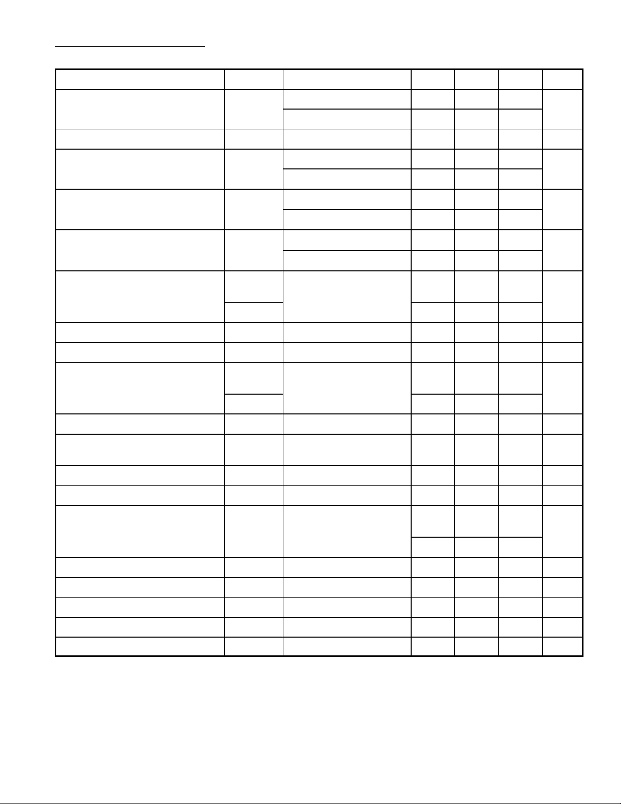
Electrical Characteristics: (V+ = 15V, V– = –15V, I
specified)
Parameter Symbol Test Conditions Min Typ Max Unit
= 500µA, TA = +25°C unless otherwise
ABC
Input Offset Voltage V
Input Offset Current I
Input Bias Current I
Forward Transconductance g
IO
IO
I
m
(Large signal)
Peak Output Current IOM
Peak Output Voltage:
Positive
Negative V–
Amplifier Supply Current I
Device Dissipation P
V+
OM
OM
A
D
Input Offset Voltage Sensitivity:
Positive
∆VIO/∆V+ – – 150 µV/V
– 0.4 5.0 mV
TA = 0 to +70°C – – 6.0
– 0.12 0.6 µA
– 2 5 µA
TA = 0 to +70°C – – 7
6700 9600 13000
µmho
TA = 0 to +70°C 5400 – –
RL = 0 350 500 650
µA
RL = 0, TA = 0 to +70°C 300 – –
RL = ∞ 12.0 13.5 – V
–12 –14.4 –
0.8 1 1.2 mA
24 30 36 mW
Negative ∆VIO/∆V– – – 150
Common–Mode Rejection Ratio CMRR 80 110 – dB
Common–Mode Input Voltage
Range
Input Resistance R
Amplifier Bias Voltage V
Slew Rate:
Maximum (uncompensated)
V
SR
ICR
I
ABC
12 to
–12
13.6 to
–14.6
– V
10 26 – kΩ
– 0.71 – V
– 75 – V/µs
Unity gain (compensated) – 50 –
Open–Loop Bandwidth BW
Input Capacitance C
Output Capacitance C
Output Resistance R
Input–to–Output Capacitance C
OL
I
O
O
I–O
f = 1MHz – 3.6 – pF
f = 1MHz – 5.6 – pF
f = 1MHz – 0.024 – pF
– 2 – MHz
– 15 – MΩ
Page 3

Pin Connection Diagram
Top View
Amplifier Bias Input
5
Output
V (+)
N.C./Tab
.177 (4.5)
7
Max
V (–)/Case
6
8
1
N.C.
4
3
Non–Inverting Input
2
Inverting Input
.370 (9.39) Dia Max
.335 (8.52) Dia Max
.492
(12.5)
Min
45°
2
1
8
7
.032 (0.82)
.018 (0.45) Dia Typ
3
4
5
6
.200 (5.06)
Dia
 Loading...