

Page 1

NTE941M & NTE941SM
Integrated Circuit
Operational Amplifier
Description:
The NTE941M and NTE941SM (Surface Mount) are general purpose operational amplifiers in
8–Lead DIP type packages and offer many features which make their application nearly foolproof:
overload protection on the input and output, no latch–up when the common mode range is exceeded,
as well as freedom from oscillators.
Absolute Maximum Ratings:
Supply Voltage, V
Differential Input Voltage, V
Common Mode Input Voltage (Note 2), V
Power Dissipation (Note 1), P
Output Short–Circuit Duration, t
Operating Temperature Range, T
Storage Temperature Range, T
Junction Temperature, T
S
ID
ICM
D
S
opr
stg
J
Lead Temperature (During Soldering, 10sec), T
Thermal Resistance, Junction–to–Ambient, R
thJA
NTE941M +100°C/W. . . . . . . . . . . . . . . . . . . . . . . . . . . . . . . . . . . . . . . . . . . . . . . . . . . . . . . . . . . . .
NTE941SM +195°C/W. . . . . . . . . . . . . . . . . . . . . . . . . . . . . . . . . . . . . . . . . . . . . . . . . . . . . . . . . . . .
Continuous. . . . . . . . . . . . . . . . . . . . . . . . . . . . . . . . . . . . . . . . . . . . . .
0° to +70°C. . . . . . . . . . . . . . . . . . . . . . . . . . . . . . . . . . . . . . . . . . .
–65° to +150°C. . . . . . . . . . . . . . . . . . . . . . . . . . . . . . . . . . . . . . . . . .
L
±18V. . . . . . . . . . . . . . . . . . . . . . . . . . . . . . . . . . . . . . . . . . . . . . . . . . . . . . . . . . . . . . . .
±30V. . . . . . . . . . . . . . . . . . . . . . . . . . . . . . . . . . . . . . . . . . . . . . . . . . . . . . .
±15V. . . . . . . . . . . . . . . . . . . . . . . . . . . . . . . . . . . . . . . . . .
500mW. . . . . . . . . . . . . . . . . . . . . . . . . . . . . . . . . . . . . . . . . . . . . . . . . . .
+100°C. . . . . . . . . . . . . . . . . . . . . . . . . . . . . . . . . . . . . . . . . . . . . . . . . . . . . . . . .
+260°C. . . . . . . . . . . . . . . . . . . . . . . . . . . . . . . . . . . .
Note 1. For operation at elevated temperatures, these devices must be derated based on thermal
resistance, and T
Max (TJ = TA + (R
J
thJA PD
).
Note 2. For supply voltage less than ±15V , the absolute maximum input voltage is equal to the supply
voltage.
Page 2
Electrical Characteristics: (VS = ±15V, 0° ≤ TA ≤ +70°C unless otherwise specified)
Parameter Symbol Test Conditions Min Typ Max Unit
Input Offset Voltage V
IO
RS ≤ 10kΩ TA = +25°C – 2.0 6.0 mV
– – 7.5 mV
Input Offset Voltage Adjustment Range V
Input Offset Current I
IOR
IO
VS = ±20V, TA = +25°C – ±15 – V
TA = +25°C – 20 200 nA
– – 300 nA
Input Bias Current I
IB
TA = +25°C – 80 500 nA
– – 0.8 µA
Input Resistance r
Common Mode Input Voltage Range V
Large Signal Voltage Gain A
Output Voltage Swing V
ICR
VS = ±20V, TA = +25°C 0.3 2.0 – MΩ
i
TA = +25°C – ±12 ±13 V
VO = ±10V,
V
RL ≥ 2kΩ
RL ≥ 10kΩ ±12 ±14 – V
O
TA = +25°C 20 200 – V/mV
15 – – V/mV
RL ≥ 2kΩ ±10 ±13 – V
Output Short–Circuit Current I
OS
TA = +25°C – 25 – mA
Common–Mode Rejection Ratio CMRR RS ≤ 10kΩ, VCM = ±12V 70 90 – dB
Supply Voltage Rejection Ratio PSRR VS = ±20V to ±5V, RS ≤ 10kΩ 77 96 – dB
Transient Response Rise Time t
TLH
TA = +25°C, Unity Gain – 0.3 – µs
Transient Response Overshoot os – 5 – %
Transient Response Slew Rate SR – 0.5 – V/µs
Supplu Current I
Power Consumption P
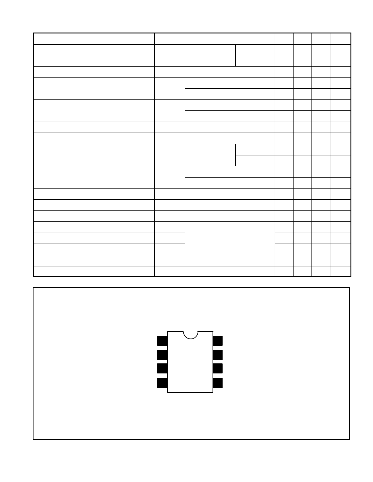
Pin Connection Diagram
Offset Null
Inverting Input
Non–Inverting Input
V (–)
1
2
3
4
D
TA = +25°C – 1.7 2.8 mA
TA = +25°C – 50 85 mW
C
8
N.C.
V (+)
7
Output
6
5 Of fset Null
Page 3

NTE941M
85
.256 (6.52) Max
14
.393 (10.0)
Max
.300 (7.62)
.192 (4.9)
.300 (7.62)
.150
(3.81)
.070 (1.77) Min.100 (2.54)
NTE941SM
.050 (1.27)
85
14
.006 (.152)
.236
(5.99)
.154
(3.91)
016
(.406)
061
(1.53)
.198 (5.03)
NOTE: Pin1 on Beveled Edge
 Loading...