

Page 1
Cascadable Silicon Bipolar
MMIC␣ Amplifier
Technical Data
MSA-1023
Features
• High Output Power:
+27 dBm Typical P
• Low Distortion:
37 dBm Typical IP3 at 1.0␣ GHz
• 8.5 dB Typical Gain at
1.0␣ GHz
• Hermetic, Metal/Beryllia
at 1.0␣ GHz
1dB
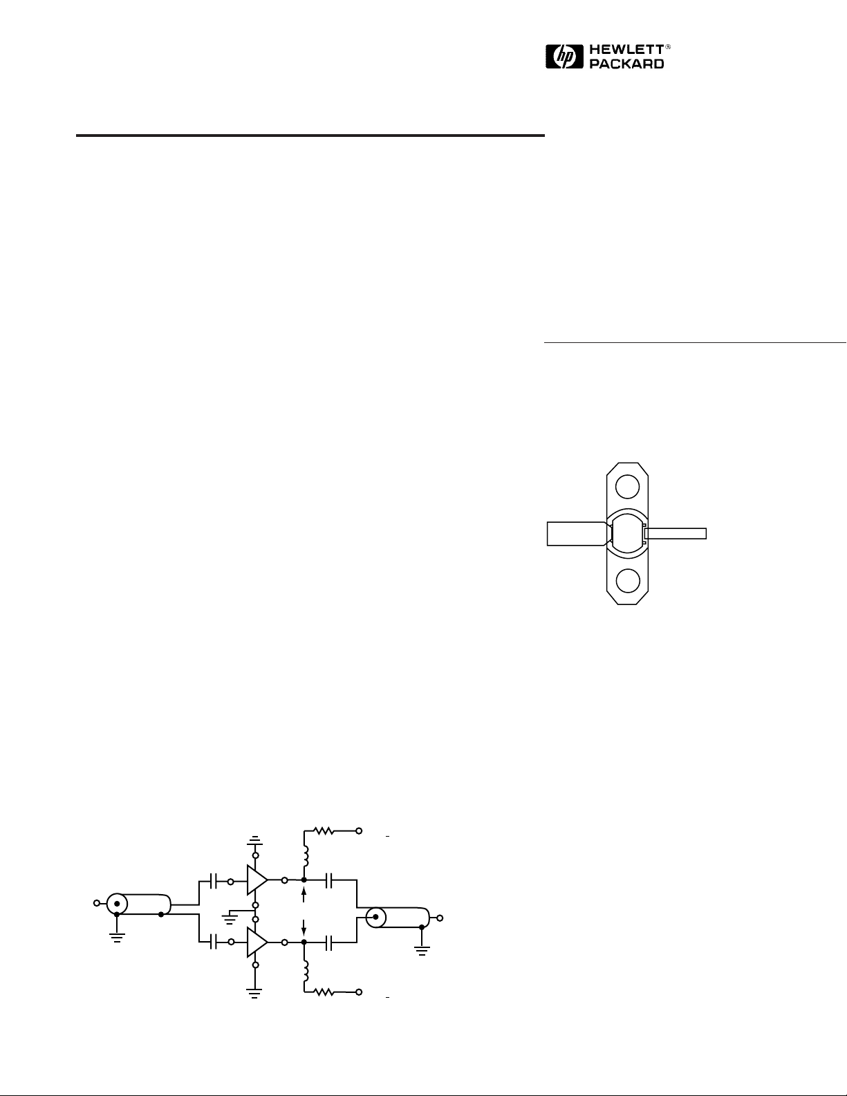
This MMIC is designed for use in a
push-pull configuration in a 25␣ Ω
system. The MSA-1023 can also be
used as a single-ended amplifier in
a 50␣ Ω system with slightly
reduced performance. Typical
applications include narrow and
broadband RF amplifiers in
industrial and military systems.
Stripline Package
• Impedance Matched to 25 Ω
for Push-Pull Configurations
The MSA-series is fabricated using
HP’s 10 GHz fT, 25␣ GHz f
silicon bipolar MMIC process
which uses nitride self-alignment,
Description
The MSA-1023 is a high performance, medium power silicon
bipolar Monolithic Microwave
Integrated Circuit (MMIC) housed
in a hermetic, BeO flange package
for good thermal characteristics.
ion implantation, and gold metallization to achieve excellent
performance, uniformity and
reliability. The use of an external
bias resistor for temperature and
current stability also allows bias
flexibility.
Typical Push-Pull Biasing Configuration
R
bias
C
block
IN
50 Ω
C
block
4
MSA
1
2
4
1
MSA
2
RFC
C
block
3
V
= 15 V
d
3
C
block
RFC
R
bias
V
>
20
CC
50 Ω
V
>
20
CC
230 mil BeO Flange Package
,
MAX
V
OUT
V
5965-9554E
6-446
Page 2
MSA-1023 Absolute Maximum Ratings
Parameter Absolute Maximum
Device Current 425 mA
Power Dissipation
RF Input Power +25 dBm
Junction Temperature 200°C
Storage Temperature –65 to 200° C
Notes:
1. Permanent damage may occur if any of these limits are exceeded.
2. T
3. Derate at 66.7 mW/°C for T
4. The small spot size of this technique results in a higher, though more
= 25°C.
CASE
accurate determination of θ
MENTS section “Thermal Resistance” for more information.
[2,3]
7.0 W
> 95°C.
C
than do alternate methods. See MEASURE-
jc
[1]
Thermal Resistance
θjc = 15°C/W
[2,4]
:
[2]
[1]
, T
= 25° C
A
= 25 Ω Units Min. Typ. Max.
O
GHz 2.5
Electrical Specifications
Symbol Parameters and Test Conditions: Id = 325 mA, Z
G
∆G
f
3 dB
P
Power Gain (|S21|2) f = 1.0 GHz dB 7.5 8.5 9.5
Gain Flatness f = 0.1 to 2.0 GHz dB ±0.6
P
3 dB Bandwidth
Input VSWR f = 0.1 to 2.0 GHz 2.0:1
VSWR
Output VSWR f = 0.1 to 2.0 GHz 2.8:1
NF 25 Ω Noise Figure f = 1.0 GHz dB 7.0
P
IP
t
V
1 dB
3
D
d
Output Power at 1 dB Gain Compression f = 1.0 GHz dBm 25.0 27.0
Third Order Intercept Point f = 1.0 GHz dBm 37.0
Group Delay f = 1.0 GHz psec 250
Device Voltage V 13.5 15.0 16.5
dV/dT Device Voltage Temperature Coefficient mV/°C –18.0
Notes:
1. The recommended operating current range for this device is 150 to 400 mA. Typical performance as a function of
current is on the following page.
Referenced from 10 MHz gain (GP).
2.
6-447
Page 3

MSA-1023 Typical Scattering Parameters (Z
Freq.
S
11
S
21
= 50 Ω, TA = 25° C, I
O
S
12
S
= 325 mA)
d
22
GHz Mag Ang dB Mag Ang dB Mag Ang Mag Ang k
0.001 .40 –121 15.3 5.85 149 –17.9 .128 22 .42 –99 0.69
0.005 .51 –167 8.5 2.67 156 –15.9 .160 6 .45 –161 1.05
0.010 .52 –174 7.5 2.36 166 –15.8 .162 3 .45 –171 1.16
0.025 .52 –178 7.2 2.28 172 –15.8 .162 1 .45 –177 1.20
0.050 .52 179 7.1 2.26 173 –15.8 .161 –1 .45 –179 1.21
0.100 .53 176 7.0 2.25 170 –15.8 .161 –3 .45 179 1.21
0.200 .53 172 7.0 2.25 163 –15.8 .161 –5 .46 174 1.21
0.400 .51 164 7.0 2.24 146 –15.8 .161 –11 .46 170 1.22
0.600 .48 157 7.0 2.24 130 –16.0 .159 –16 .45 165 1.23
0.800 .45 151 7.0 2.23 113 –16.1 .157 –21 .44 161 1.24
1.000 .42 146 7.0 2.23 95 –16.2 .155 –26 .44 157 1.24
1.200 .38 144 6.9 2.22 78 –16.4 .151 –31 .44 155 1.24
1.400 .35 145 6.8 2.20 61 –16.7 .146 –36 .45 154 1.24
1.600 .34 149 6.6 2.15 44 –17.0 .141 –41 .46 153 1.22
1.800 .36 152 6.3 2.07 19 –17.3 .136 –45 .49 150 1.18
2.000 .39 153 5.9 1.97 11 –17.7 .130 –49 .62 148 1.13
2.500 .51 148 4.6 1.69 –24 –18.3 .121 –52 .52 140 .91
3.000 .60 133 3.0 1.41 –57 –17.9 .127 –57 .70 128 .59
A model for this device is available in the DEVICE MODELS section.
Typical Performance, T
(unless otherwise noted)
10
1.0 GHz
1.5 GHz
1.0 GHz,
4.0 GHz
0.5 GHz
0.5 GHz
1.0 GHz
2.0 GHz
8
6
GAIN (dB)
4
2
0
2.0 GHz
1816 20 22 26 2824 30 32
POWER OUT (dBm)
Figure 1. Typical Gain vs. Power Out,
ZO = 25°Ω, Id = 325 mA.
32
30
28
26
(dBm)
1 dB
P
24
22
20
+25–50 +100
TEMPERATURE (°C)
Figure 4. Output Power at 1 dB Gain
Compression vs. Temperature,
= 25 Ω, Id = 325 mA.
Z
O
= 25° C
A
400
TC = +100°C
T
= +25°C
C
T
= –50°C
C
300
200
(mA)
d
I
100
0
2046810
(V)
V
d
Figure 2. Device Current vs. Voltage.
10
8
6
(dB)
4
GAIN
2
0
0.1 0.2 0.3 0.5 2.01.0 4.0
Id = 400 mA
Id = 325 mA
= 150 mA
I
d
ZO = 50 Ω
FREQUENCY (GHz)
ZO = 25 Ω
Figure 5. Gain vs. Frequency,
Id = 325 mA.
6-448
40
36
(dBm)
3
32
28
24
(dBm) IP
1 dB
P
20
200150 250 300 350 400
(mA)
I
d
Figure 3. Output Power at 1 dB
Gain Compression, Third Order
Intercept Point vs. Current,
=25Ω, f = 1.0 GHz.
Z
O
6
5
4
Input ZO = 50 Ω
3
VSWR
Output Z
= 50 Ω
2
1
0
0.1 0.2 0.3 0.5 2.01.0 3.0
O
Input ZO = 25 Ω
Output Z
= 25 Ω
O
FREQUENCY (GHz)
Figure 6. VSWR vs. Frequency,
Id = 325 mA.
IP
3
P
1 dB
Page 4

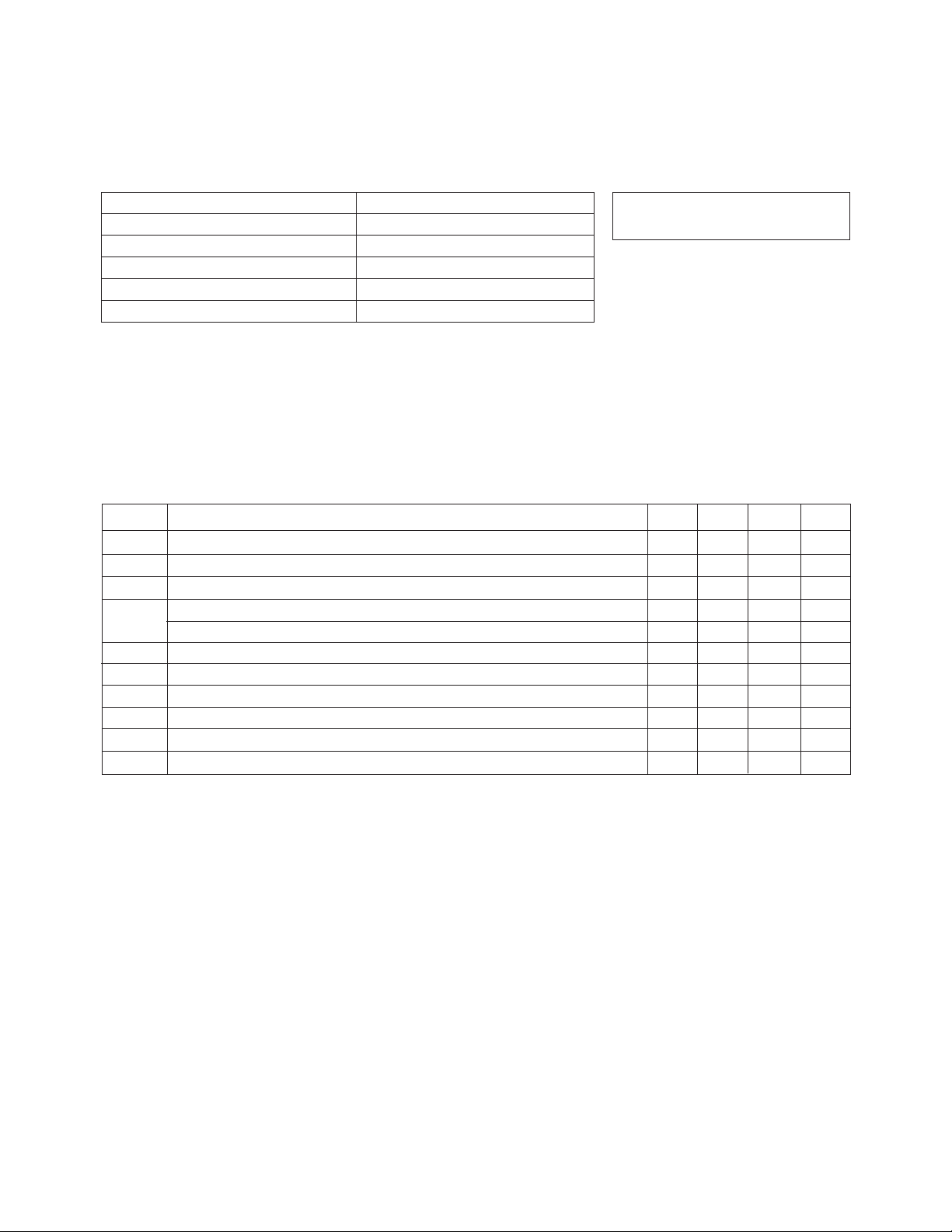
230 mil BeO Flange Package
.725 ± .030
18.42 ± .76
20.32
.562
14.27
.130 ± .010
3.30 ± .25
.004 ± .002
.10 ± .05
.800
RF
INPUT
1
.120
3.05
.130
3.30
4
2
.230
5.84
GROUND
.050
3
.060
1.52
1.27
in
mm
RF OUTPUT
AND BIAS
GROUND
Notes:
(unless otherwise specified)
1. Dimensions are
2. Tolerances
in .xxx = ± 0.005
mm .xx = ± 0.13
6-449
 Loading...