

Page 1
Cascadable Silicon Bipolar
MMIC␣ Amplifier
Technical Data
MSA-0686
Features
• Cascadable 50 Ω Gain Block
• Low Operating Voltage:
3.5 V Typical V
• 3 dB Bandwidth:
DC to 0.8 GHz
• High Gain:
18.5␣ dB Typical at 0.5 GHz
• Low Noise Figure:
3.0 dB Typical at 0.5 GHz
• Surface Mount Plastic
Package
• Tape-and-Reel Packaging
Available
Note:
1. Refer to PACKAGING section “Tapeand-Reel Packaging for Surface
Mount Semiconductors”.
d
[1]
The MSA-0686 is a high performance silicon bipolar Monolithic
Microwave Integrated Circuit
(MMIC) housed in a low cost,
surface mount plastic package.
This MMIC is designed for use as a
general purpose 50 Ω gain block.
Applications include narrow and
broad band IF and RF amplifiers
in commercial and industrial
applications.
The MSA-series is fabricated using
HP’s 10 GHz fT, 25␣ GHz f
MAX
,
silicon bipolar MMIC process
which uses nitride self-alignment,
ion implantation, and gold metallization to achieve excellent
performance, uniformity and
reliability. The use of an external
bias resistor for temperature and
current stability also allows bias
flexibility.
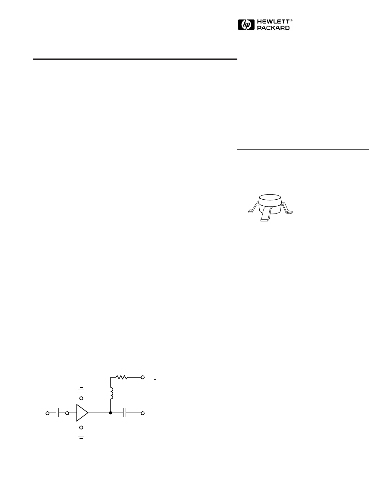
86 Plastic PackageDescription
Typical Biasing Configuration
R
bias
RFC (Optional)
C
block
IN OUT
4
3
MSA
1
2
V
= 3.5 V
d
C
block
5965-9588E
V
CC
> 5 V
6-382
Page 2
MSA-0686 Absolute Maximum Ratings
Parameter Absolute Maximum
Device Current 50 mA
Power Dissipation
[2,3]
200 mW
RF Input Power +13 dBm
Junction Temperature 150°C
Storage Temperature –65 to 150° C
Notes:
1. Permanent damage may occur if any of these limits are exceeded.
CASE
= 25°C.
> 126° C.
C
2. T
3. Derate at 8.3 mW/° C for T
4. See MEASUREMENTS section “Thermal Resistance” for more information.
[1]
Thermal Resistance
θjc = 120°C/W
[2,4]
:
Electrical Specifications
Symbol Parameters and Test Conditions: Id = 16 mA, Z
G
P
Power Gain (|S21|2) f = 0.1 GHz dB 20.0
[1]
, T
A
= 25° C
= 50 Ω Units Min. Typ. Max.
O
f = 0.5 GHz 16.5 18.5
∆G
f
3 dB
VSWR
Gain Flatness f = 0.1 to 0.5 GHz dB ±0.7
P
3 dB Bandwidth GHz 0.8
Input VSWR f = 0.1 to 1.5 GHz 1.7:1
Output VSWR f = 0.1 to 1.5 GHz 1.7:1
NF 50 Ω Noise Figure f = 0.5 GHz dB 3.0
P
IP
t
V
1 dB
3
D
d
Output Power at 1 dB Gain Compression f = 0.5 GHz dBm 2.0
Third Order Intercept Point f = 0.5 GHz dBm 14.5
Group Delay f = 0.5 GHz psec 225
Device Voltage V 2.8 3.5 4.2
dV/dT Device Voltage Temperature Coefficient mV/°C –8.0
Notes:
1. The recommended operating current range for this device is 12 to 20 mA. Typical performance as a function of current
is on the following page.
Part Number Ordering Information
Part Number No. of Devices Container
MSA-0686-TR1 1000 7" Reel
MSA-0686-BLK 100 Antistatic Bag
For more information, see “Tape and Reel Packaging for Semiconductor Devices”.
6-383
Page 3

MSA-0686 Typical Scattering Parameters (Z
G
p
(dB)
0.1 0.3 0.5 1.0 3.0 6.0
FREQUENCY (GHz)
Figure 1. Typical Power Gain vs.
Frequency, TA = 25°C.
102345
V
d
(V)
Figure 2. Device Current vs. Voltage.
0
3
6
9
12
15
18
24
21
0
5
10
15
20
25
Gain Flat to DC
I
d
(mA)
TC = +85°C
T
C
= +25°C
T
C
= –25°C
0.1 0.2 0.3 0.5 2.01.0 4.0
FREQUENCY (GHz)
Figure 4. Output Power at 1 dB Gain
Compression vs. Frequency.
–4
0
4
8
12
P
1 dB
(dBm)
Id = 20 mA
Id = 30 mA
Id = 12 mA
I
d
= 16 mA
I
d
= 25 mA
Id = 12 mA
Id = 16 mA
2.5
2.0
3.0
3.5
4.0
NF (dB)
FREQUENCY (GHz)
Figure 5. Noise Figure vs. Frequency.
0.1 0.2 0.3 0.5 2.01.0 4.0
0
1
2
3
4
5
0
1
2
3
4
5
17
18
19
20
–25 +250 +55 +85
P
1 dB
(dBm)
NF (dB)
Gp (dB)
TEMPERATURE (°C)
Figure 3. Output Power at 1 dB Gain
Compression, NF and Power Gain vs.
Case Temperature, f = 1.0 GHz,
I
d
=16mA.
P
1 dB
NF
G
P
Id= 12 mA
I
d
= 16 mA, 30 mA
I
d
= 20 mA
Freq.
S
11
S
21
= 50 Ω, TA = 25° C, I
O
S
12
S
= 16 mA)
d
22
GHz Mag Ang dB Mag Ang dB Mag Ang Mag Ang k
0.1 .06 –175 20.1 10.08 170 –23.3 .069 4 .04 –84 1.05
0.2 .06 –169 19.8 9.77 161 –23.2 .069 8 .07 –103 1.05
0.3 .07 –164 19.4 9.35 152 –22.5 .075 13 .10 –113 1.03
0.4 .08 –158 19.1 8.98 144 –22.2 .078 16 .13 –123 1.02
0.5 .08 –154 18.7 8.58 135 –21.6 .083 18 .15 –131 1.01
0.6 .09 –152 18.0 7.94 128 –21.1 .088 21 .18 –140 1.01
0.8 .12 –152 17.2 7.25 114 –20.3 .097 25 .21 –155 1.00
1.0 .15 –154 16.3 6.51 102 –19.5 .106 25 .24 –168 0.99
1.5 .25 –171 14.0 5.01 76 –17.6 .133 22 .27 165 0.99
2.0 .34 171 11.9 3.94 56 –16.1 .157 19 .27 147 1.01
2.5 .43 155 9.8 3.09 42 –15.9 .161 16 .27 134 1.06
3.0 .49 140 8.0 2.51 28 –15.3 .171 11 .26 124 1.10
3.5 .56 128 6.4 2.09 15 –15.1 .175 6 .25 118 1.13
4.0 .61 118 5.0 1.78 3 –14.9 .180 3 .24 115 1.15
5.0 .70 99 2.4 1.32 –18 –14.7 .185 –2 .24 118 1.16
Note:
1. A model for this device is available in the DEVICE MODELS section.
Typical Performance, T
(unless otherwise noted)
= 25° C
A
6-384
Page 4

86 Plastic Package Dimensions
0.51 ± 0.13
(0.020 ± 0.005)
RF INPUT
1.52 ± 0.25
(0.060 ± 0.010)
0.66 ± 0.013
(0.026 ± 0.005)
0.30 MIN
(0.012 MIN)
GROUND
45°
1
GROUND
2.67 ± 0.38
(0.105 ± 0.15)
(0.085 ± 0.005)
DIMENSIONS ARE IN MILLIMETERS (INCHES)
A06
5° TYP.
2.16 ± 0.13
4
RF OUTPUT
AND DC BIAS
3
2.34 ± 0.38
(0.092 ± 0.015)
2
(0.006 ± 0.002)
8° MAX
0° MIN
0.203 ± 0.051
C
L
6-385
 Loading...