

Page 1
MIC5204 Micrel
MIC5204
SCSI-II Active Terminator
Preliminary Information
General Description
The MIC5204 is an active terminator designed to comply with
SCSI-II specifications. The MIC5204 is enabled by a CMOS
or TTL compatible logic signal. When disabled, power
consumption drops nearly to zero and the output goes into a
high impedance state. Key MIC5204 features include protection against reversed battery, current limiting, and overtemperature shutdown.
Ordering Information
Features
• ± 1% output voltage accuracy
• Guaranteed 500mA output
• Low quiescent current
• Low dropout voltage
• Extremely tight load and line regulation
• Very low temperature coefficient
• Current and thermal limiting
• Zero off-mode current
• Logic-controlled electronic shutdown
• Available in SO-8 and SOT-223 packages
2
Applications
• SCSI-II active terminator
• Desktop, laptop, notebook, and palmtop computers
• Intelligent instrumentation
• Printers
• Disk drives
• Voltage reference
Pin Configuration
Part Number Junction Temp. Range Package
MIC5204BM –40°C to +125°C SO-8
MIC5204BS –40°C to +125°C SOT-223
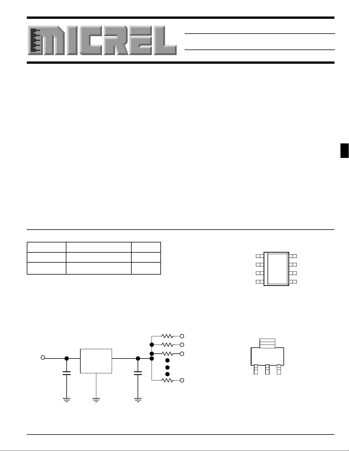
T ypical Application
+
MIC5204
+
22µF10µF
+5V
110Ω
110Ω
110Ω
110Ω
SCSI Bus
18 to 27
Lines
V
OUT
V
OUT
NC
GROUND
V
IN
V
IN
NC
ENABLE
MIC5204BM
Both VIN and both V
together. ENABLE must be pulled high for
operation.
1 2 3
IN GND OUT
MIC5204-xxBS
pins must be tied
OUT
TAB IS GROUND
February 1999 59 MIC5204
Page 2

MIC5204 Micrel
Absolute Maximum Ratings (Note 1)
Input Voltage (VIN) ........................................ –20V to +20V
Enable Input Voltage (VEN) .......................... –0.3V to +20V
Power Dissipation (PD)................Internally Limited, Note 3
Operating Ratings (Note 2)
Input Voltage (VIN) ............................................ +3V to +6V
Enable Input Voltage (VEN) ............................. –0.3V to V
Junction Temperature Range (TJ) ........... –40°C to +125°C
Lead Temperature (soldering, 5 sec.) ....................... 260°C
ESD Rating .............................................................>2000V
Electrical Characteristics
VIN = V
Symbol Parameter Conditions Min Typical Max Units
V
O
∆V
O
∆V
O/VIN
∆V
O/IL
+ 1V; IL = 1mA; CL = 3.3µF; VEN ≥ 2.0V; TJ = 25°C, bold values indicate –40°C ≤ TJ ≤ +125°C; unless noted.
OUT
Output Voltage Accuracy 2.821 2.85 2.87 V
2.793 2.907
/∆T Output Voltage Note 4 20 100 ppm/°C
Temperature Coef.
Line Regulation VIN = V
+ 1V to 6V 0.004 0.10 %
OUT
0.40
Load Regulation IL = 0.1mA to 100mA, Note 5 0.04 0.16 %
0.30
IN
VIN–V
O
Dropout Voltage, Note 6 IL = 100µA30mV
75
IL = 50mA 190
240
= 100mA 210
I
L
350
IL = 500mA 450
750
I
Q
I
GND
Quiescent Current V
Ground Pin Current V
≤ 0.7V (Shutdown) 0.01 µA
ENABLE
≥ 2.0V, IL = 100µA 130 µA
ENABLE
= 20mA 240
I
L
I
= 30mA 300
L
= 50mA 450
I
L
IL = 100mA 900
PSRR Ripple Rejection 70 dB
I
GNDDO
Ground Pin VIN = 0.5V less than designed V
OUT
270 330 µA
Current at Dropout IL = 100µA, Note 7
I
LIMIT
∆V
e
n
O
/∆P
D
Current Limit V
= 0V 750 mA
OUT
Thermal Regulation Note 8 0.05 %/W
Output Noise 30 µV
Enable Input
Input Voltage Level
V
IL
Logic Low off 0.7 V
Logic High on 2.0
I
IL
I
IH
Enable Input Current VIL ≤ 0.7V 0.01 µA
VIH ≥ 2.0V 15 50
February 1999 60 MIC5204
Page 3

Note 1. Exceeding the absolute maximum rating may damage the device.
3.0
3.5
4.0
4.5
5.0
5.5
6.0
-50 -25 0 25 50 75 100 125
GROUND CURRENT (mA)
JUNCTION TEMPERATURE (˚C)
Note 2. The device is not guaranteed to function outside its operating rating.
Note 3. The maximum allowable power dissipation is a function of the maximum junction temperature, T
resistance, θJA, and the ambient temperature, TA. The maximum allowable power dissipation at any ambient temperature is calculated using:
P
= (T
(max)
go into thermal shutdown. The θJC of the MIC5204BS is 15°C/W and θJA for the MIC5204BM is 160°C/W mounted on a PC board (see
J(max)–TA
) θJA. Exceeding the maximum allowable power dissipation will result in excessive die temperature, and the regulator will
, the junction-to-ambient thermal
J(max)
“Thermal Considerations” for details).
Note 4. Output voltage temperature coefficient is defined as the worst case voltage change divided by the total temperature range.
Note 5. Regulation is measured at constant junction temperature using low duty cycle pulse testing. Parts are tested for load regulation in the load
range from 0.1mA to 100mA. Changes in output voltage due to heating effects are covered by the thermal regulation specification.
Note 6. Dropout Voltage is defined as the input to output differential at which the output voltage drops 2% below its nominal value measured at 1V
differential.
Note 7. Ground pin current is the regulator quiescent current plus pass transistor base current. The total current drawn from the supply is the sum of
the load current plus the ground pin current.
Note 8. Thermal regulation is defined as the change in output voltage at a time “t” after a change in power dissipation is applied, excluding load or line
regulation effects. Specifications are for a 500mA load pulse at VIN = 6V for t = 10ms.
T ypical Characteristics
Output Voltage Variation
vs. Junction Temperature
1.0
0.8
0.6
0.4
0.2
0.0
-0.2
-0.4
-0.6
-0.8
-1.0
OUTPUT VOLTAGE VARIATION (%)
-50 -25 0 25 50 75 100 125
JUNCTION TEMPERATURE (˚C)
Ground Current
vs. Junction Temperature
RL = 20Ω
= 6V
V
IN
Page 4

MIC5204 Micrel
Thermal ConsiderationsApplications Information
External Capacitors
A 2.2µF capacitor is recommended between the MIC5204
output and ground to prevent oscillations due to instability.
Larger values serve to improve the regulator's transient response. Most types of tantalum or aluminum electrolytics will
be adequate; film types will work. Many aluminum electrolytics
have electrolytes that freeze at about –30°C, so solid tantalums
are recommended for operation below –25°C. The important
parameters of the capacitor are an effective series resistance
of about 5Ω or less and a resonant frequency above 500kHz.
The value of this capacitor may be increased without limit.
A 1µF capacitor should be placed from the MIC5204 input to
ground if there is more than 10 inches of wire between the
input and the AC filter capacitor or if a battery is used as the
input.
The MIC5204 will remain stable and in regulation with no load
in addition to the internal voltage divider.
Part I. Layout
The MIC5204BM (8-pin surface mount package) has the
following thermal characteristics when mounted on a single
layer copper-clad printed circuit board.
PC Board
Dielectric
FR4 160°C/W
Ceramic 120°C/W
θθ
θ
θθ
JA
Multi-layer boards having a ground plane, wide traces near
the pads, and large supply bus lines provide better thermal
conductivity. The "worst case" value of 160°C/W assumes no
ground plane, minimum trace widths, and a FR4 material
board.
Part II. Nominal Power Dissipation and Die Temperature
The MIC5204BM at a 25°C ambient temperature will operate
reliably at up to 625mW power dissipation when mounted in
the "worst case" manner described above. At an ambient
temperature of 55°C, the device may safely dissipate 440mW.
These power levels are equivalent to a die temperature of
125°C, the recommended maximum temperature for nonmilitary grade silicon integrated circuits. In normal SCSI
terminator applications, the average power dissipation is very
small and this minimum geometry heat sink is suitable. The
total dissipation does not approact the 400mW to 625mW
range described above.
For MIC5204BS (SOT-223 package) heat sink characteristics, please refer to Micrel Application Hint 17, “P.C. Board
Heat Sinking”. As with the SO-8, average power dissipation
in SCSI terminator applications is low and a minimum pad size
is generally adequate.
50 mil
245 mil
30 mil 50 mil
150 mil
Minimum recommended board pad size, SO-8.
February 1999 62 MIC5204
 Loading...