

Page 1
MIC5209 Micrel
MIC5209
500mA Low-Noise LDO Regulator
General Description
The MIC5209 is an efficient linear voltage regulator with very
low dropout voltage, typically 10mV at light loads and less
than 500mV at full load, with better than 1% output voltage
accuracy.
Designed especially for hand-held, battery-powered devices,
the MIC5209 features low ground current to help prolong
battery life. An enable/shutdown pin on SO-8 and TO-263-5
versions can further improve battery life with near-zero shutdown current.
Key features include reversed-battery protection, current
limiting, overtemperature shutdown, ultra-low-noise capability (SO-8 and TO-263-5 versions), and availability in thermally efficient packaging. The MIC5209 is available in adjustable or fixed output voltages.
For space-critical applications where peak currents do not
exceed 500mA, see the MIC5219.
Features
• Meets Intel® Slot 1 and Slot 2 requirements
• Guaranteed 500mA output over the full operating
temperature range
• Low 500mV maximum dropout voltage at full load
• Extremely tight load and line regulation
• Thermally-efficient surface-mount package
• Low temperature coefficient
• Current and thermal limiting
• Reversed-battery protection
• No-load stability
• 1% output accuracy
• Ultra-low-noise capability in SO-8 and TO-263-5
Applications
• Pentium II Slot 1 and Slot 2 support circuits
• Laptop, notebook, and palmtop computers
• Cellular telephones
• Consumer and personal electronics
• SMPS post-regulator/dc-to-dc modules
• High-efficiency linear power supplies
Typical Applications
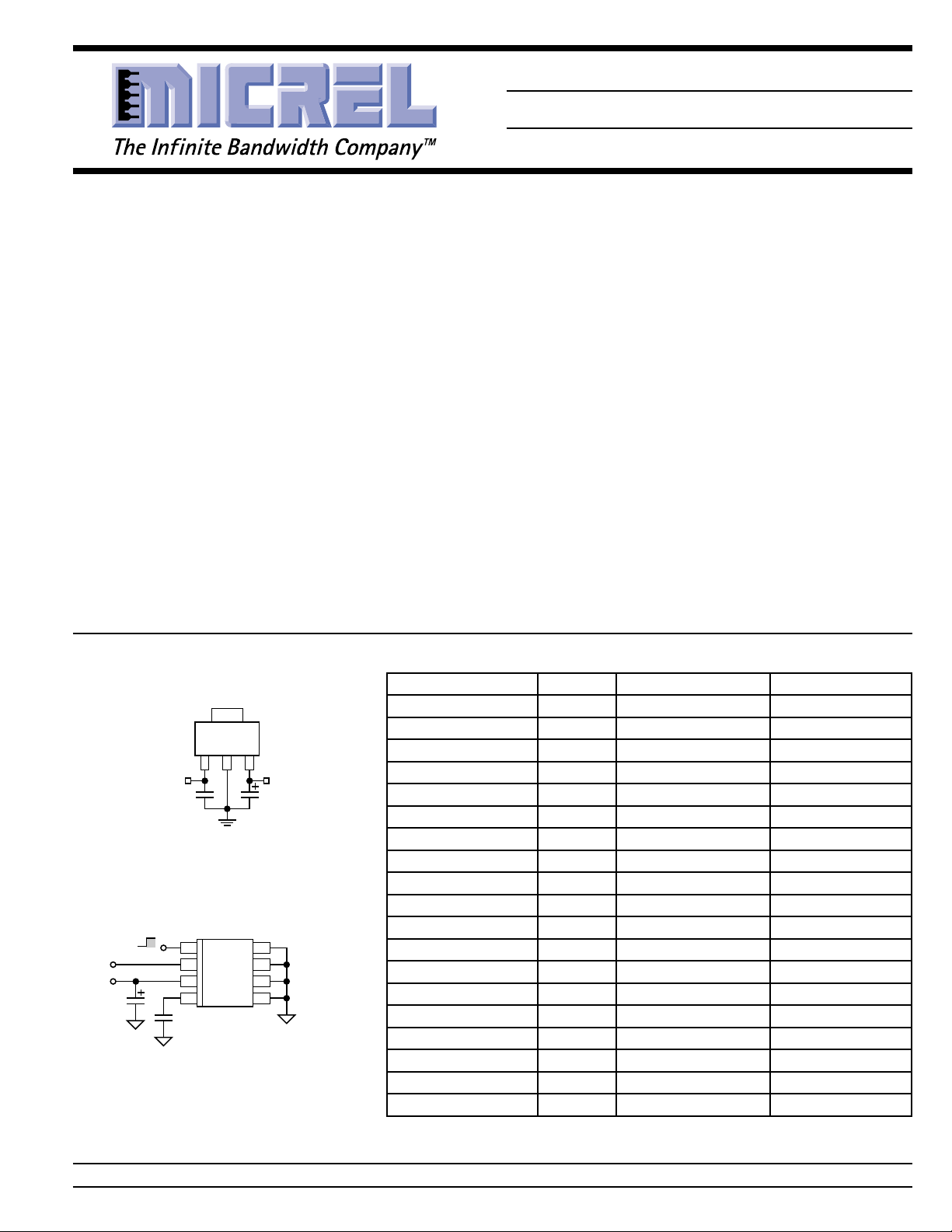
MIC5209-2.5BS
132
V
IN
≥ 3.0V
0.1µF
3.3V Nominal-Input Slot-1
Power Supply
ENABLE
SHUTDOWN
V
IN
6V
V
OUT
5V
2.2µF
tantalum
MIC5209-5.0BM
1
2
3
4
470pF
(OPTIONAL)
Ultra-Low-Noise 5V Regulator
22µF
tantalum
V
OUT
2.5V ±1%
8
7
6
5
Ordering Information
Part Number Voltage Junct. Temp. Range Package
MIC5209-2.5BS 2.5V –40°C to +125°C SOT-223
MIC5209-3.0BS 3.0V –40°C to +125°C SOT-223
MIC5209-3.3BS 3.3V –40°C to +125°C SOT-223
MIC5209-3.6BS 3.6V –40°C to +125°C SOT-223
MIC5209-4.2BS 4.2V –40°C to +125°C SOT-223
MIC5209-5.0BS 5.0V –40°C to +125°C SOT-223
MIC5209-1.8BM 1.8V 0°C to +125°C SO-8
MIC5209-2.5BM 2.5V –40°C to +125°C SO-8
MIC5209-3.0BM 3.0V –40°C to +125°C SO-8
MIC5209-3.3BM 3.3V –40°C to +125°C SO-8
MIC5209-3.6BM 3.6V –40°C to +125°C SO-8
MIC5209-5.0BM 5.0V –40°C to +125°C SO-8
MIC5209BM Adj. –40°C to +125°C SO-8
MIC5209-2.5BU 2.5V –40°C to +125°C TO-263-5
MIC5209-3.0BU 3.0V –40°C to +125°C TO-263-5
MIC5209-3.3BU 3.3V –40°C to +125°C TO-263-5
MIC5209-3.6BU 3.6V –40°C to +125°C TO-263-5
MIC5209-5.0BU 5.0V –40°C to +125°C TO-263-5
MIC5209BU Adj. –40°C to +125°C TO-263-5
Micrel, Inc. • 1849 Fortune Drive • San Jose, CA 95131 • USA • tel + 1 (408) 944-0800 • fax + 1 (408) 944-0970 • http://www.micrel.com
August 2, 2000 1 MIC5209
Page 2
MIC5209 Micrel
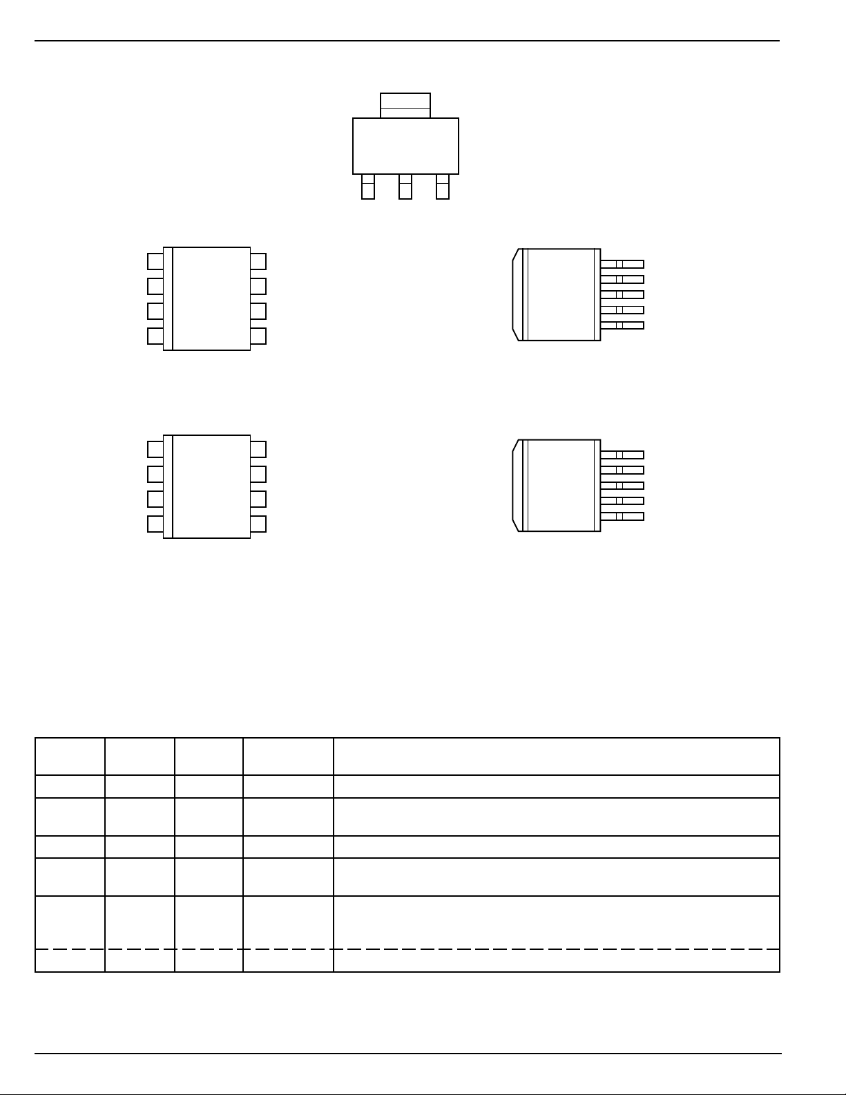
Pin Configuration
GND
TAB
132
IN OUTGND
MIC5209-x.xBS
EN
IN
OUT
BYP
1
2
3
4
GND
8
GND
7
GND
6
GND
5
SOT-223
Fixed Voltages
TAB
GND
5 BYP
4 OUT
3 GND
2IN
1EN
MIC5209-x.xBM
SO-8
TO-263-5
Fixed Voltages
Fixed Voltages
MIC5209-x.xBU
EN
1
IN
2
OUT
3
ADJ
4
MIC5209BM
Adjustable Voltage
SO-8
GND
8
GND
7
TAB
GND
6
GND
5
GND
5 ADJ
4 OUT
3 GND
2IN
1EN
MIC5209BU
TO-263-5
Adjustable Voltage
Pin Description
Pin No. Pin No. Pin No. Pin Name Pin Function
SOT-223 SO-8 TO-263-5
1 2 2 IN Supply Input
TAB 5–8 3 GND Ground: SOT-223 pin 2 and TAB are internally connected. SO-8 pins 5
2,
through 8 are internally connected.
3 3 4 OUT Regulator Output
1 1 EN Enable (Input): CMOS compatible control input. Logic high = enable; logic
low or open = shutdown.
4 (fixed) 5 (fixed) BYP Reference Bypass: Connect external 470pF capacitor to GND to reduce
output noise. May be left open. For 1.8V or 2.5V operation, see “Applica-
tions Information.”
4 (adj.) 5 (adj.) ADJ Adjust (Input): Feedback input. Connect to resistive voltage-divider network.
MIC5209 2 August 2, 2000
Page 3
MIC5209 Micrel
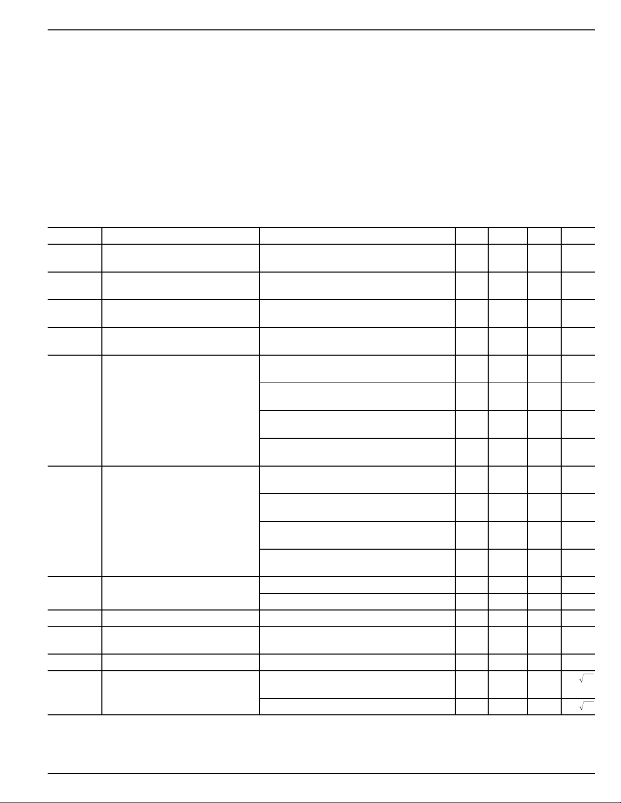
Absolute Maximum Ratings (Note 1)
Supply Input Voltage (V
Power Dissipation (P
Junction Temperature (T
all except 1.8V......................................–40°C to +125°C
1.8V only ..................................................0°C to +125°C
Lead Temperature (soldering, 5 sec.) ....................... 260°C
Storage Temperature (T
) ............................ –20V to +20V
IN
) ............... Internally Limited, Note 3
D
)
J
) ....................... –65°C to +150°C
S
Operating Ratings (Note 2)
Supply Input Voltage (V
Enable Input Voltage (V
Junction Temperature (TJ)
all except 1.8V......................................–40°C to +125°C
1.8V only ..................................................0°C to +125°C
Package Thermal Resistance .................................. Note 3
) ........................... +2.5V to +16V
IN
) .................................. 0V to V
EN
Electrical Characteristics
VIN = V
0°C ≤ TJ ≤ +125°C for 1.8V version; unless noted.
Symbol Parameter Conditions Min Typical Max Units
V
OUT
∆V
OUT
∆V
OUT/VOUT
∆V
OUT/VOUT
V
IN
I
GND
I
GND
PSRR Ripple Rejection f = 120Hz 75 dB
I
LIMIT
∆V
OUT
e
no
+ 1.0V; C
OUT
Output Voltage Accuracy variation from nominal V
= 4.7µF, I
OUT
= 100µA; TJ = 25°C, bold values indicate –40°C ≤ TJ ≤ +125°C except
OUT
OUT
–11%
–2 2 %
/∆T Output Voltage Note 4 40 ppm/°C
Temperature Coefficient
– V
OUT
Line Regulation VIN = V
Load Regulation I
Dropout Voltage, Note 6 I
OUT
OUT
+ 1V to 16V 0.009 0.05 %/V
OUT
0.1 %/V
= 100µA to 500mA, Note 5 0.05 0.5 %
0.7 %
= 100µA1060mV
80 mV
I
= 50mA 115 175 mV
OUT
250 mV
I
= 150mA 165 300 mV
OUT
400 mV
I
= 500mA 350 500 mV
OUT
600 mV
Ground Pin Current, Notes 7, 8 VEN ≥ 3.0V, I
= 100µA80130µA
OUT
170 µA
V
≥ 3.0V, I
EN
= 50mA 350 650 µA
OUT
900 µA
V
≥ 3.0V, I
EN
= 150mA 1.8 2.5 mA
OUT
3.0 mA
V
≥ 3.0V, I
EN
= 500mA 8 20 mA
OUT
25 mA
Ground Pin Quiescent Current, VEN ≤ 0.4V (shutdown) 0.05 3 µA
Note 8
Current Limit V
VEN ≤ 0.18V (shutdown) 0.10 8 µA
= 0V 700 900 mA
OUT
1000 mA
/∆P
Thermal Regulation Note 9 0.05 %/W
D
Output Noise V
Note 10 C
OUT
OUT
I
= 50mA, C
OUT
= 2.5V, I
= 2.2µF, C
OUT
= 50mA, 500
= 0
BYP
= 2.2µF, C
OUT
= 470pF 300
BYP
nV/ Hz
nV/ Hz
IN
August 2, 2000 3 MIC5209
Page 4

MIC5209 Micrel
ENABLE Input
V
ENL
I
ENL
I
ENH
Note 1. Exceeding the absolute maximum rating may damage the device.
Note 2. The device is not guaranteed to function outside its operating rating.
Note 3: The maximum allowable power dissipation at any TA (ambient temperature) is calculated using: P
Note 4: Output voltage temperature coefficient is the worst case voltage change divided by the total temperature range.
Note 5: Regulation is measured at constant junction temperature using low duty cycle pulse testing. Parts are tested for load regulation in the load
Note 6: Dropout voltage is defined as the input to output differential at which the output voltage drops 2% below its nominal value measured at 1V
Note 7: Ground pin current is the regulator quiescent current plus pass transistor base current. The total current drawn from the supply is the sum of
Note 8: VEN is the voltage externally applied to devices with the EN (enable) input pin. [SO-8 (M) and TO-263-5 (U) packages only.]
Note 9: Thermal regulation is the change in output voltage at a time “t” after a change in power dissipation is applied, excluding load or line regulation
Note 10: C
Enable Input Logic-Low Voltage VEN = logic low (regulator shutdown) 0.4 V
0.18 V
VEN = logic high (regulator enabled) 2.0 V
Enable Input Current V
maximum allowable power dissipation will result in excessive die temperature, and the regulator will go into thermal shutdown. See Table 1
and the “Thermal Considerations” section for details.
range from 100µA to 500mA. Changes in output voltage due to heating effects are covered by the thermal regulation specification.
differential.
the load current plus the ground pin current.
effects. Specifications are for a 500mA load pulse at VIN = 16V for t = 10ms.
is an optional, external bypass capacitor connected to devices with a BYP (bypass) or ADJ (adjust) pin. [SO-8 (M) and TO-263-5 (U)
BYP
packages only].
≤ 0.4V 0.01 –1 µA
ENL
V
≤ 0.18V 0.01 –2 µA
ENL
V
≥ 2.0V 5 20 µA
ENH
D(max)
= (T
– TA) ÷ θJA. Exceeding the
J(max)
25 µA
MIC5209 4 August 2, 2000
Page 5
MIC5209 Micrel
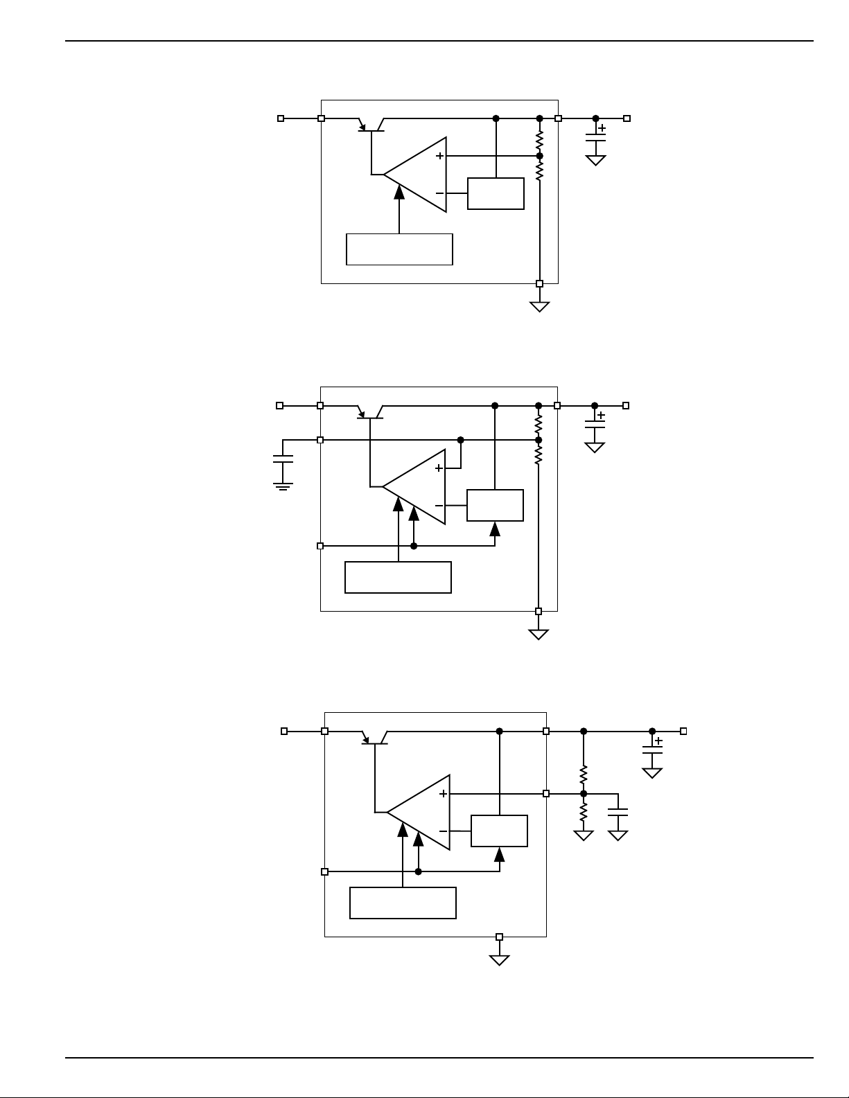
Block Diagrams
V
IN
V
IN
C
BYP
(optional)
IN
OUT
Bandgap
Ref.
Current Limit
Thermal Shutdown
MIC5209-x.xBS
GND
Low-Noise Fixed Regulator (SOT-223 version only)
IN
BYP
EN
Bandgap
Ref.
V
REF
OUT
V
OUT
C
OUT
V
OUT
C
OUT
Current Limit
Thermal Shutdown
MIC5209-x.xBM/U
GND
Ultra-Low-Noise Fixed Regulator
V
IN
IN
Bandgap
Ref.
V
REF
EN
Current Limit
Thermal Shutdown
MIC5209BM/U [adj.]
GND
OUT
ADJ
R1
R2
C
C
BYP
(optional)
OUT
V
OUT
Ultra-Low-Noise Adjustable Regulator
August 2, 2000 5 MIC5209
Page 6
MIC5209 Micrel
√
√
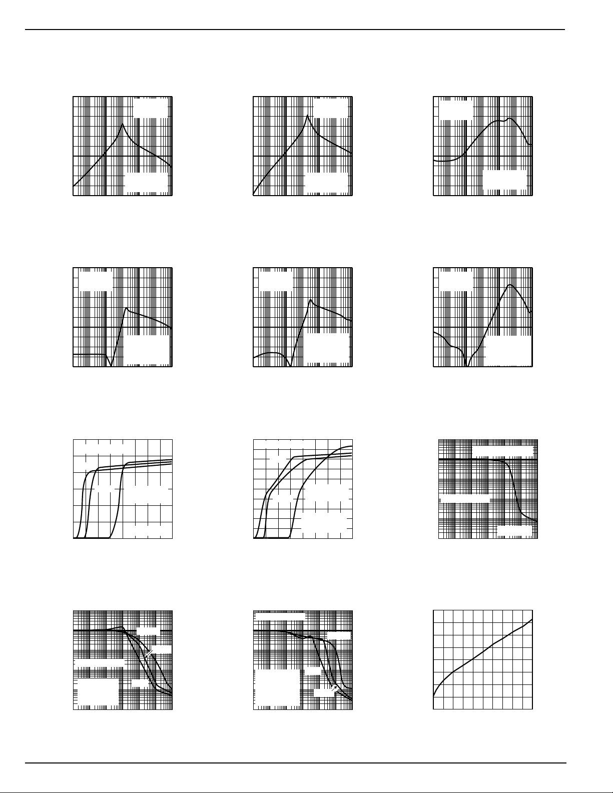
Typical Characteristics
Power Supply
Rejection Ratio
0
-20
VIN = 6V
V
= 5V
OUT
-40
-60
PSRR (dB)
-80
-100
1E+11E+21E+3 1E+41E+51E+6 1E+7
10
100
FREQUENCY (Hz)
I
= 100µA
OUT
C
= 1µF
OUT
1k
10k
100k
Power Supply
Rejection Ratio
0
VIN = 6V
V
-20
-40
-60
PSRR (dB)
-80
-100
= 5V
OUT
I
= 100µA
OUT
C
= 2.2µF
OUT
C
= 0.01µF
BYP
1E+11E+21E+3 1E+41E+51E+6 1E+7
10
1k
100
10k
FREQUENCY (Hz)
100k
1M
1M
10M
10M
Power Supply
Rejection Ratio
0
-20
VIN = 6V
V
= 5V
OUT
-40
-60
PSRR (dB)
-80
-100
1E+11E+21E+3 1E+41E+51E+6 1E+7
10
100
FREQUENCY (Hz)
I
= 1mA
OUT
C
= 1µF
OUT
1k
10k
100k
1M
Power Supply
Rejection Ratio
0
VIN = 6V
V
-20
-40
-60
PSRR (dB)
-80
-100
= 5V
OUT
I
= 1mA
OUT
C
= 2.2µF
OUT
C
= 0.01µF
BYP
1E+11E+21E+3 1E+41E+51E+6 1E+7
10
1k
100
10k
FREQUENCY (Hz)
100k
1M
10M
10M
Power Supply
Rejection Ratio
0
VIN = 6V
V
OUT
= 5V
-20
-40
-60
PSRR (dB)
I
10k
C
OUT
OUT
= 100mA
= 1µF
100k
1M
-80
-100
1E+11E+21E+3 1E+41E+51E+6 1E+7
10
1k
100
FREQUENCY (Hz)
Power Supply
Rejection Ratio
0
VIN = 6V
V
-20
-40
-60
PSRR (dB)
-80
-100
= 5V
OUT
I
= 100mA
OUT
C
= 2.2µF
OUT
C
= 0.01µF
BYP
1E+11E+21E+3 1E+41E+51E+6 1E+7
10
1k
100
10k
FREQUENCY (Hz)
100k
1M
10M
10M
Power Supply Ripple Rejection
vs. Voltage Drop
60
500mA pending
50
1mA
40
30
20
10
RIPPLE REJECTION (dB)
10mA
I
= 100mA
OUT
C
= 1µF
0
0 0.1 0.2 0.3 0.4
VOLTAGE DROP (V)
OUT
Power Supply Ripple Rejection
100
RIPPLE REJECTION (dB)
vs. Voltage Drop
500mA pending
90
80
1mA
70
60
50
40
10mA
30
20
10
0
0 0.1 0.2 0.3 0.4
VOLTAGE DROP (V)
I
C
OUT
C
BYP
= 100mA
OUT
= 2.2µF
= 0.01µF
Noise Performance
10
10mA, C
1
OUT
0.1
500mA Pending
0.01
NOISE (µV/√Hz)
0.001
V
0.0001
10
1E+11E+21E+3 1E+41E+51E+61E+7
1k
100
10k 100k 1M 10M
FREQUENCY (Hz)
OUT
= 1µF
= 5V
Dropout Voltage
Noise Performance
10
1
Hz)
0.1
500mA Pending
0.01
NOISE (µV/
V
= 5V
OUT
0.001
C
= 10µF
OUT
electrolytic
0.0001
10
1E+11E+21E+31E+4 1E+51E+61E+7
1k
100
FREQUENCY (Hz)
100mA
10mA
1mA
10k 100k1M10M
Hz)
NOISE (µV/
0.001
0.0001
Noise Performance
10
500mA Pending
1
100mA
0.1
0.01
V
= 5V
OUT
C
= 10µF
OUT
electrolytic
C
= 100pF
BYP
10
1E+11E+21E+31E+4 1E+51E+61E+7
100
FREQUENCY (Hz)
1mA
10mA
1k
10k 100k1M10M
vs. Output Current
400
300
200
100
DROPOUT VOLTAGE (mV)
0
0 100 200 300 400 500
OUTPUT CURRENT (mA)
MIC5209 6 August 2, 2000
Page 7
MIC5209 Micrel
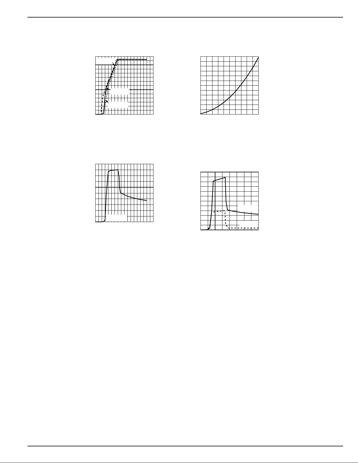
Dropout Characteristics
3.5
IL =100µA
3.0
2.5
2.0
1.5
1.0
OUTPUT VOLTAGE (V)
0.5
0
IL=100mA
IL=500mA
0123456789
INPUT VOLTAGE (V)
Ground Current
vs. Supply Voltage
25
20
15
10
5
GROUND CURRENT (mA)
IL=500mA
0
0123456789
INPUT VOLTAGE (V)
Ground Current
vs. Output Current
12
10
8
6
4
2
GROUND CURRENT (mA)
0
0 100 200 300 400 500
OUTPUT CURRENT (mA)
Ground Current
vs. Supply Voltage
3.0
2.5
2.0
1.5
1.0
0.5
GROUND CURRENT (mA)
0
02468
INPUT VOLTAGE (V)
IL=100 mA
IL=100µA
August 2, 2000 7 MIC5209
Page 8
MIC5209 Micrel
Applications Information
Enable/Shutdown
Enable is available only on devices in the SO-8 (M) and
TO-263-5 (U) packages.
Forcing EN (enable/shutdown) high (> 2V) enables the regulator. EN is compatible with CMOS logic. If the enable/
shutdown feature is not required, connect EN to IN (supply
input).
Input Capacitor
A 1µF capacitor should be placed from IN to GND if there is
more than 10 inches of wire between the input and the ac filter
capacitor or if a battery is used as the input.
Output Capacitor
An output capacitor is required between OUT and GND to
prevent oscillation. The minimum size of the output capacitor
is dependent upon whether a reference bypass capacitor is
used. 1µF minimum is recommended when C
(see Figure 1). 2.2µF minimum is recommended when C
is 470pF (see Figure 2). Larger values improve the regulator’s
transient response.
The output capacitor should have an ESR (equivalent series
resistance) of about 5Ω and a resonant frequency above
1MHz. Ultra-low-ESR capacitors can cause a low amplitude
oscillation on the output and/or underdamped transient response. Most tantalum or aluminum electrolytic capacitors
are adequate; film types will work, but are more expensive.
Since many aluminum electrolytics have electrolytes that
freeze at about –30°C, solid tantalums are recommended for
operation below –25°C.
At lower values of output current, less output capacitance is
needed for output stability. The capacitor can be reduced to
0.47µF for current below 10mA or 0.33µF for currents below
1mA.
No-Load Stability
The MIC5209 will remain stable and in regulation with no load
(other than the internal voltage divider) unlike many other
voltage regulators. This is especially important in CMOS
RAM keep-alive applications.
Reference Bypass Capacitor
BYP (reference bypass) is available only on devices in SO-8
and TO-263-5 packages.
BYP is connected to the internal voltage reference. A 470pF
capacitor (C
) connected from BYP to GND quiets this
BYP
reference, providing a significant reduction in output noise
(ultra-low-noise performance). Because C
phase margin, the output capacitor should be increased to at
least 2.2µF to maintain stability.
The start-up speed of the MIC5209 is inversely proportional
to the size of the reference bypass capacitor. Applications
requiring a slow ramp-up of output voltage should consider
larger values of C
consider omitting C
If output noise is not critical, omit C
. Likewise, if rapid turn-on is necessary,
BYP
.
BYP
and leave BYP open.
BYP
is not used
BYP
reduces the
BYP
BYP
Thermal Considerations
The SOT-223 has a ground tab which allows it to dissipate
more power than the SO-8. Refer to “Slot-1 Power Supply” for
details. At 25°C ambient, it will operate reliably at 2W dissipation with “worst-case” mounting (no ground plane, minimum
trace widths, and FR4 printed circuit board).
Thermal resistance values for the SO-8 represent typical
mounting on a 1"-square, copper-clad, FR4 circuit board. For
greater power dissipation, SO-8 versions of the MIC5209
feature a fused internal lead frame and die bonding arrangement that reduces thermal resistance when compared to
standard SO-8 packages.
Package
SOT-223 (S) 50°C/W 8°C/W
SO-8 (M) 50°C/W 25°C/W
TO-263-5 (U) — 2°C/W
θθ
θ
θθ
JA
θθ
θ
θθ
JC
Table 1. MIC5209 Thermal Resistance
Multilayer boards with a ground plane, wide traces near the
pads, and large supply-bus lines will have better thermal
conductivity and will also allow additional power dissipation.
For additional heat sink characteristics, please refer to Micrel
Application Hint 17, “Designing P.C. Board Heat Sinks”,
included in Micrel’s
Databook
. For a full discussion of heat
sinking and thermal effects on voltage regulators, refer to
Regulator Thermals section of Micrel’s
Dropout Voltage Regulators
handbook.
Designing with Low-
Low-Voltage Operation
The MIC5209-1.8 and MIC5209-2.5 require special consideration when used in voltage-sensitive systems. They may
momentarily overshoot their nominal output voltages unless
appropriate output and bypass capacitor values are chosen.
During regulator power up, the pass transistor is fully saturated for a short time, while the error amplifier and voltage
reference are being powered up more slowly from the output
(see “Block Diagram”). Selecting larger output and bypass
capacitors allows additional time for the error amplifier and
reference to turn on and prevent overshoot.
To ensure that no overshoot is present when starting up into
a light load (100µA), use a 4.7µF output capacitance and
470pF bypass capacitance. This slows the turn-on enough to
allow the regulator to react and keep the output voltage from
exceeding its nominal value. At heavier loads, use a 10µF
output capacitance and 470pF bypass capacitance. Lower
values of output and bypass capacitance can be used,
depending on the sensitivity of the system.
Applications that can withstand some overshoot on the
output of the regulator can reduce the output capacitor and/
or reduce or eliminate the bypass capacitor. Applications that
are not sensitive to overshoot due to power-on reset delays
can use normal output and bypass capacitor configurations.
Please note the junction temperature range of the regulator
at 1.8V output (fixed and adjustable) is 0˚C to +125˚C.
MIC5209 8 August 2, 2000
Page 9
MIC5209 Micrel
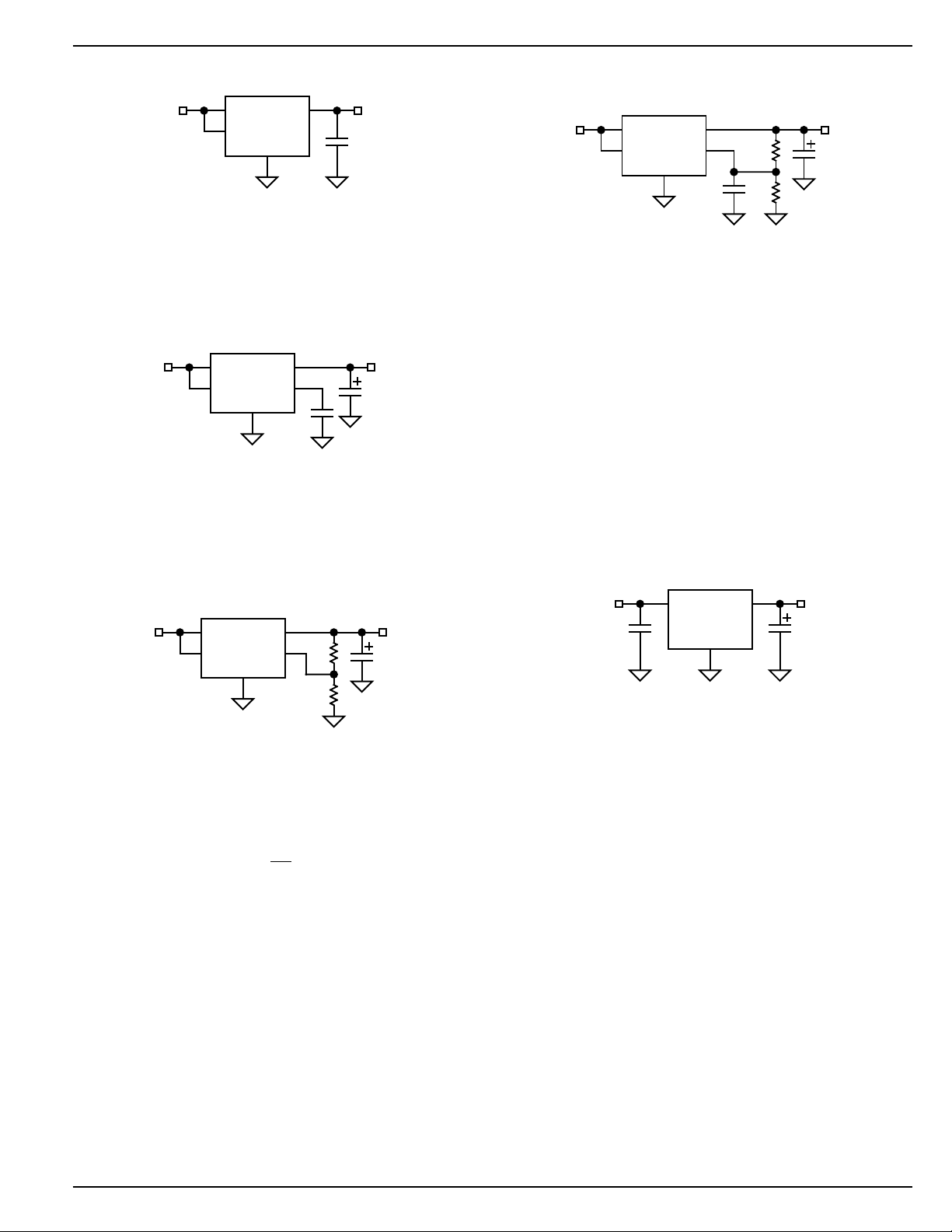
Fixed Regulator Circuits
MIC5209-x.xBM
V
IN
2
IN OUT
1
EN BYP
GND
5–8
V
OUT
3
4
1µF
Figure 1. Low-Noise Fixed Voltage Regulator
Figure 1 shows a basic MIC5209-x.xBM (SO-8) fixed-voltage
regulator circuit. See Figure 5 for a similar configuration
using the more thermally-efficient MIC5209-x.xBS (SOT-223).
A 1µF minimum output capacitor is required for basic fixedvoltage applications.
MIC5209-x.xBM
V
IN
2
IN OUT
1
EN BYP
3
4
GND
5–8
470pF
V
OUT
2.2µF
Figure 2. Ultra-Low-Noise Fixed Voltage Regulator
Figure 2 includes the optional 470pF noise bypass capacitor
between BYP and GND to reduce output noise. Note that the
minimum value of C
must be increased when the bypass
OUT
capacitor is used.
Adjustable Regulator Circuits
IN
MIC5209BM
2
IN OUT
1
EN ADJ
GND
5–8
V
3
4
R1
OUT
1µF
R2
V
Although ADJ is a high-impedance input, for best performance, R2 should not exceed 470kΩ.
IN
MIC5209BM
2
IN OUT
1
EN ADJ
GND
5–8
3
4
470pF
R1
R2
V
OUT
2.2µF
V
Figure 4. Ultra-Low-Noise Adjustable Application.
Figure 4 includes the optional 470pF bypass capacitor from
ADJ to GND to reduce output noise.
Slot-1 Power Supply
Intel’s Pentium II processors have a requirement for a 2.5V
±5% power supply for a clock synthesizer and its associated
loads. The current requirement for the 2.5V supply is dependant upon the clock synthesizer used, the number of clock
outputs, and the type of level shifter (from core logic levels to
2.5V levels). Intel estimates a worst-case load of 320mA.
The MIC5209 was designed to provide the 2.5V power
requirement for Slot-1 applications. Its guaranteed performance of 2.5V ±3% at 500mA allows adequate margin for all
systems, and its dropout voltage of 500mV means that it
operates from a worst-case 3.3V supply where the voltage
can be as low as 3.0V.
IN
C
IN
MIC5209-x.xBS
1
IN OUT
GND
2,TAB
V
OUT
3
C
OUT
22µF
V
0.1µF
Figure 5. Slot-1 Power Supply
Figure 3. Low-Noise Adjustable Voltage Regulator
The MIC5209BM/U can be adjusted to a specific output
voltage by using two external resistors (Figure 3). The resistors set the output voltage based on the equation:
R2
R1
V = 1.242V +
OUT
1
This equation is correct due to the configuration of the
bandgap reference. The bandgap voltage is relative to the
output, as seen in the block diagram. Traditional regulators
normally have the reference voltage relative to ground;
therefore, their equations are different from the equation for
the MIC5209BM/U.
A Slot-1 power supply (Figure 5) is easy to implement. Only
two capacitors are necessary, and their values are not critical.
CIN bypasses the internal circuitry and should be at least
0.1µF. C
provides output filtering, improves transient
OUT
response, and compensates the internal regulator control
loop. Its value should be at least 22µF. CIN and C
OUT
may be
increased as much as desired.
Slot-1 Power Supply Power Dissipation
Powered from a 3.3V supply, the Slot-1 power supply of
Figure 5 has a nominal efficiency of 75%. At the maximum
anticipated Slot 1 load (320mA), the nominal power dissipation is only 256mW.
The SOT-223 package has sufficient thermal characteristics
for wide design margins when mounted on a single layer
copper-clad printed circuit board. The power dissipation of
August 2, 2000 9 MIC5209
Page 10
MIC5209 Micrel
the MIC5209 is calculated using the voltage drop across the
device × output current plus supply voltage × ground current.
Considering worst case tolerances, the power dissipation
could be as high as:
(V
IN(max)
– V
OUT(max)
) × I
OUT
+ V
IN(max)
× I
GND
[(3.6V – 2.375V) × 320mA] + (3.6V × 4mA)
PD = 407mW
Using the maximum junction temperature of 125°C and a θ
JC
of 8°C/W for the SOT-223, 25°C/W for the SO-8, or 2°C/W for
the TO-263 package, the following worst-case heat-sink
thermal resistance (θSA) requirements are:
T T
θ
JA
θθθ
SA
T
A
θ
(limit) 209°C/W 184°C/W 160°C/W 123°C/W
JA
J(max) A
=
=−
JA
θSA SOT-223 201°C/W 176°C/W 152°C/W 115°C/W
θSA SO-8 184°C/W 159°C/W 135°C/W 98°C/W
θSA TO-263-5 207°C/W 182°C/W 158°C/W 121°C/W
−
P
D
JC
40°C50°C60°C75°C
Table 2. Maximum Allowable Thermal Resistance
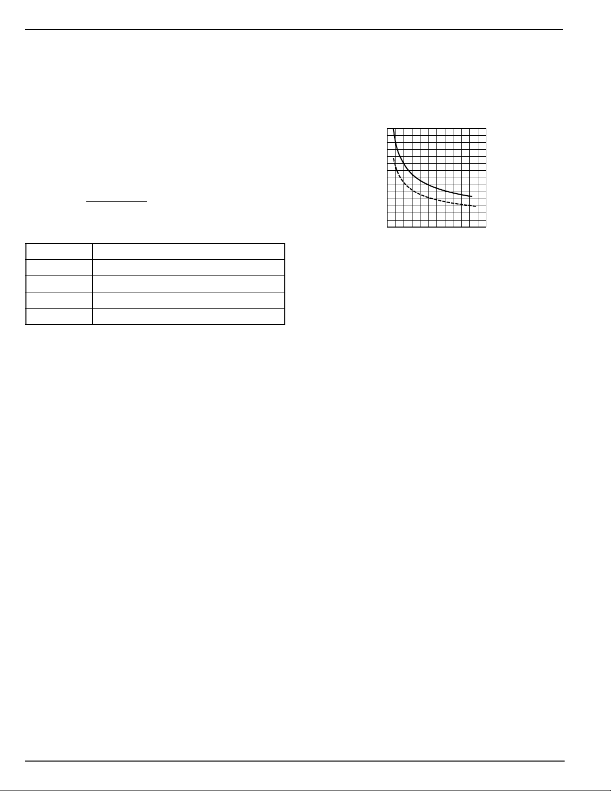
Table 2 and Figure 6 show that the Slot-1 power supply
application can be implemented with a minimum footprint
layout. Figure 6 shows the necessary copper pad area to
obtain specific heat sink thermal resistance (θSA) values. The
θ
values in Table 2 require much less than 500mm2 of
SA
copper, according to Figure 6, and can easily be accomplished with the minimum footprint.
70
60
50
40
30
20
10
THERMAL RESISTANCE (°C/W)
0
0 2000 4000 6000
COPPER HEAT SINK AREA (mm2)
Figure 6. PCB Heat Sink Thermal Resistance
MIC5209 10 August 2, 2000
Page 11
MIC5209 Micrel
16°
10°
0.84 (0.033)
0.64 (0.025)
1.04 (0.041)
0.85 (0.033)
2.41 (0.095)
2.21 (0.087)
4.7 (0.185)
4.5 (0.177)
6.70 (0.264)
6.30 (0.248)
7.49 (0.295)
6.71 (0.264)
3.71 (0.146)
3.30 (0.130)
3.15 (0.124)
2.90 (0.114)
10°
MAX
0.10 (0.004)
0.02 (0.0008)
0.038 (0.015)
0.25 (0.010)
C
L
DIMENSIONS:
MM (INCH)
C
L
1.70 (0.067)
1.52 (0.060)
0.91 (0.036) MIN
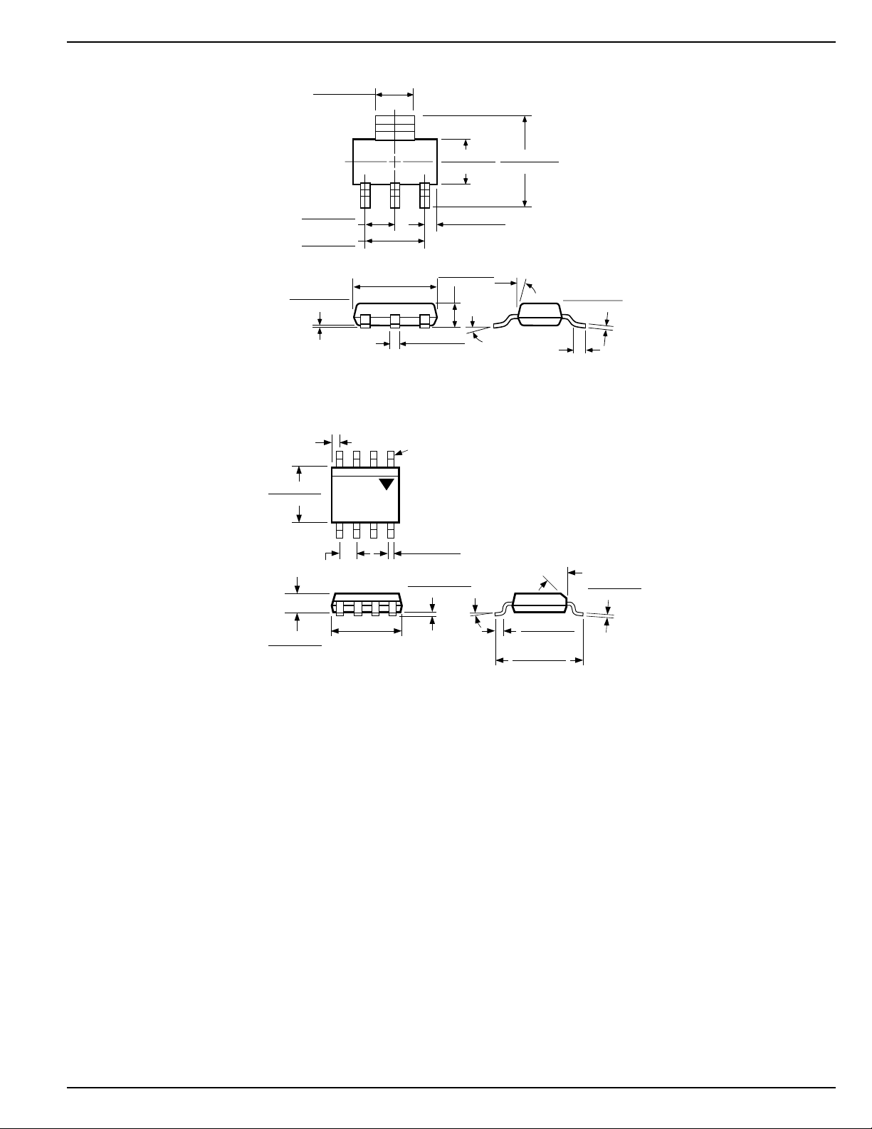
Package Information
SOT-223 (S)
0.026 (0.65)
MAX)
PIN 1
0.157 (3.99)
0.150 (3.81)
0.050 (1.27)
0.064 (1.63)
0.045 (1.14)
TYP
0.197 (5.0)
0.189 (4.8)
0.020 (0.51)
0.013 (0.33)
0.0098 (0.249)
0.0040 (0.102)
SEATING
PLANE
0°–8°
DIMENSIONS:
INCHES (MM)
0.050 (1.27)
0.016 (0.40)
0.244 (6.20)
0.228 (5.79)
45°
0.010 (0.25)
0.007 (0.18)
8-Pin SOP (M)
August 2, 2000 11 MIC5209
Page 12
MIC5209 Micrel
0.405±0.005
0.065±0.010
20°±2°
0.067±0.005 0.032 ±0.003
DIM. = INCH
0.050±0.005
0.360±0.005
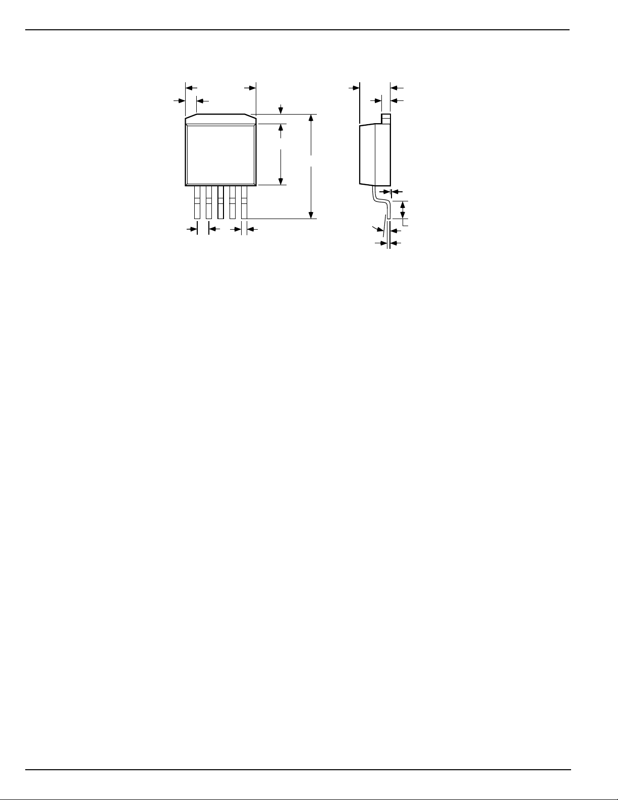
TO-263-5 (U)
0.600±0.025
8° MAX
0.015 ±0.002
0.176±0.005
0.060±0.005
SEATING PLANE
+0.004
0.004
–0.008
0.100±0.01
MIC5209 12 August 2, 2000
Page 13

MIC5209 Micrel
MICREL INC. 1849 FORTUNE DRIVE SAN JOSE, CA 95131 USA
TEL + 1 (408) 944-0800 FAX + 1 (408) 944-0970 WEB http://www.micrel.com
This information is believed to be accurate and reliable, however no responsibility is assumed by Micrel for its use nor for any infringement of patents or
other rights of third parties resulting from its use. No license is granted by implication or otherwise under any patent or patent right of Micrel Inc.
© 2000 Micrel Incorporated
August 2, 2000 13 MIC5209
 Loading...