

Page 1
MIC5206 Micrel
MIC5206
150mA Low-Noise LDO Regulator
General Description
The MIC5206 is an efficient linear voltage regulator with very
low dropout voltage (typically 17mV at light loads and 165mV
at 150mA), and very low ground current (600µA at 100mA
output), with better than 1% initial accuracy. It has a logic
compatible enable/shutdown control input and an internal
undervoltage monitor.
Designed especially for hand-held, battery-powered devices,
the MIC5206 can be switched by a CMOS or TTL compatible
logic signal. When disabled, power consumption drops
nearly to zero. Dropout ground current is minimized to
prolong battery life.
Key features include an undervoltage monitor with an error
flag output, a reference bypass pin to improve its already lownoise performance (8-lead versions only), reversed-battery
protection, current limiting, and overtemperature shutdown.
The MIC5206 is available in several fixed voltages in a tiny
SOT-23-5 package. It features a pinout, similar to the LP2980,
but has significantly better performance. Fixed and adjustable output voltage versions, featuring the reference bypass
option, are available in the 8-lead Micrel Mini 8™ 8-lead
MSOP (micro small-outline package).
For low-dropout regulators that are stable with ceramic
output capacitors, see the µCap MIC5245/6/7 family.
Features
• Error flag indicates undervoltage fault
• High output voltage accuracy
• Guaranteed 150mA output
• Ultra-low-noise output (8-lead versions)
• Low quiescent current
• Low dropout voltage
• Extremely tight load and line regulation
• Very low temperature coefficient
• Current and thermal limiting
• Reversed-battery protection
•“Zero” off-mode current
• Logic-controlled electronic enable
Applications
• Cellular telephones
• Laptop, notebook, and palmtop computers
• Battery-powered equipment
• PCMCIA VCC and V
• Consumer/personal electronics
• SMPS post-regulator/dc-to-dc modules
• High-efficiency linear power supplies
regulation/switching
PP
Typical Applications
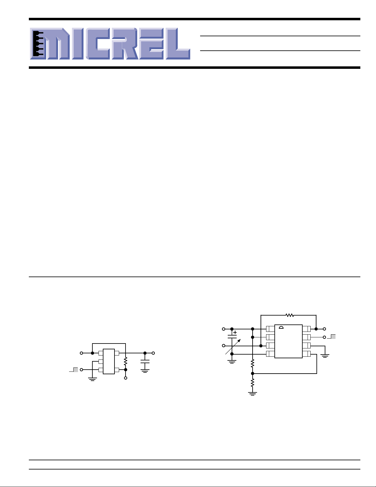
47k
MIC5206BMM
V
Enable
Shutdown
Enable (pin 3) may be
connected directly to
Supply Input (pin 1).
MIC5206-x.xBM5
IN
15
2
34
V
100k
Flag Output
(optional)
OUT
C
OUT
1µF tantalum
V
OUT
Flag Output
(optional)
tantalum
1µF
1
2
3
4
R1
R2
SOT-23-5 Fixed Voltage Application Adjustable Voltage Application
Micrel Mini 8™ is a trademark of Micrel, Inc.
Micrel, Inc. • 1849 Fortune Drive • San Jose, CA 95131 • USA • tel + 1 (408) 944-0800 • fax + 1 (408) 944-0970 • http://www.micrel.com
January 2000 1 MIC5206
8
V
7
6
5
IN
Enable (pin 7) may be
connected directly to
Supply Input (pin 8).
Enable
Shutdown
Page 2
MIC5206 Micrel
Ordering Information
Part Number Marking Volts Accuracy Junction Temp. Range Package
MIC5206-2.5BM5 LD25 2.5 1% –40°C to +125°C SOT-23-5
MIC5206-2.7BM5 LD27 2.7 1% –40°C to +125°C SOT-23-5
MIC5206-3.0BM5 LD30 3.0 1% –40°C to +125°C SOT-23-5
MIC5206-3.2BM5 LD32 3.2 1% –40°C to +125°C SOT-23-5
MIC5206-3.3BM5 LD33 3.3 1% –40°C to +125°C SOT-23-5
MIC5206-3.6BM5 LD36 3.6 1% –40°C to +125°C SOT-23-5
MIC5206-3.8BM5 LD38 3.8 1% –40°C to +125°C SOT-23-5
MIC5206-4.0BM5 LD40 4.0 1% –40°C to +125°C SOT-23-5
MIC5206-5.0BM5 LD50 5.0 1% –40°C to +125°C SOT-23-5
MIC5206BMM — Adj 1% –40°C to +125°C 8-lead MSOP
MIC5206-3.0BMM — 3.0 1% –40°C to +125°C 8-lead MSOP
MIC5206-3.3BMM — 3.3 1% –40°C to +125°C 8-lead MSOP
MIC5206-3.6BMM — 3.6 1% –40°C to +125°C 8-lead MSOP
MIC5206-3.8BMM — 3.8 1% –40°C to +125°C 8-lead MSOP
MIC5206-4.0BMM — 4.0 1% –40°C to +125°C 8-lead MSOP
MIC5206-5.0BMM — 5.0 1% –40°C to +125°C 8-lead MSOP
Other voltages available. Contact Micrel for details.
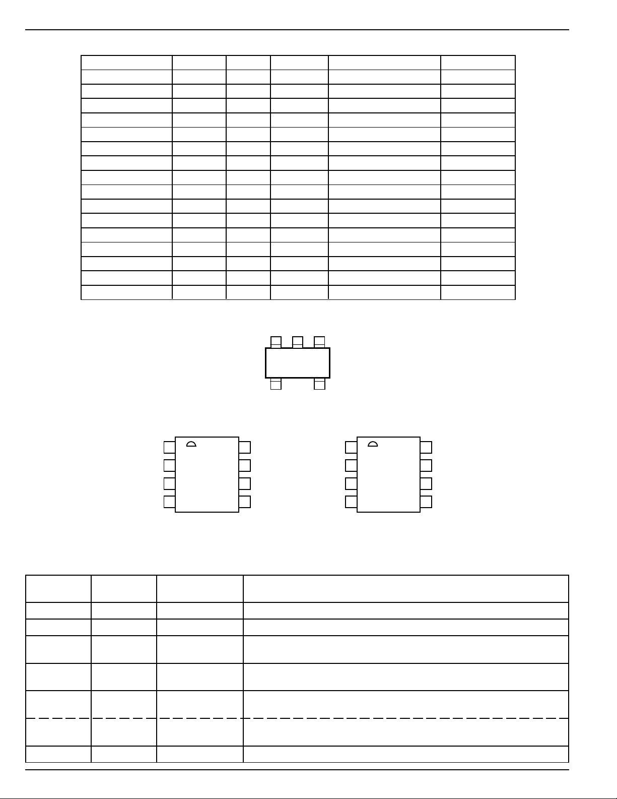
Pin Configuration
EN
GND
2
IN
13
LDxx
45
OUTFLAG
MIC5206-xxBM5
(Fixed Output Voltage)
1
OUT
2
OUT
GND
3
4
FLAG
MIC5206-x.xBMM
(Fixed Output Voltage)
8
IN
7
EN
6
GND
BYP
5
FLAG
OUT
OUT
GND
1
2
3
4
MIC5206BMM
(Adjustable Ouput Voltage)
8
IN
7
EN
6
GND
ADJ
5
Pin Description
MIC5206 MIC5206 Pin Name Pin Function
SOT-23-5 MSOP-8
1 8 IN Supply Input
2 4, 6 GND Ground
3 7 EN Enable/Shutdown (Input): CMOS compatible input. Logic high = enable,
logic low or open = shutdown. Do not leave floating.
4 3 FLAG Error Flag (Output): Open-collector output. Active low indicates an ouput
undervoltage condition.
5 (fixed) BYP Reference Bypass: Connect external 470pF capacitor to GND to reduce
output noise. May be left open.
5 (adj.) ADJ Adjust (Input): Adjustable regulator feedback input. Connect to resistor
voltage divider.
5 1,2 OUT Regulator Output
MIC5206 2 January 2000
Page 3
MIC5206 Micrel
Absolute Maximum Ratings (Note 1)
Supply Input Voltage (V
Enable Input Voltage (V
Power Dissipation (P
Junction Temperature (TJ) ....................... –40°C to +125°C
Lead Temperature (Soldering, 5 sec.) ...................... 260°C
) ............................ –20V to +20V
IN
) ........................... –20V to +20V
EN
) ............... Internally Limited, Note 3
D
Operating Ratings (Note 2)
Supply Input Voltage (V
Enable Input Voltage (V
Junction Temperature (TJ) ....................... –40°C to +125°C
SOT-23-5 (θJA).........................................................Note 3
8-lead MSOP (θ
) ................................................... Note 3
JA
) ........................... +2.5V to +16V
IN
) .................................. 0V to V
EN
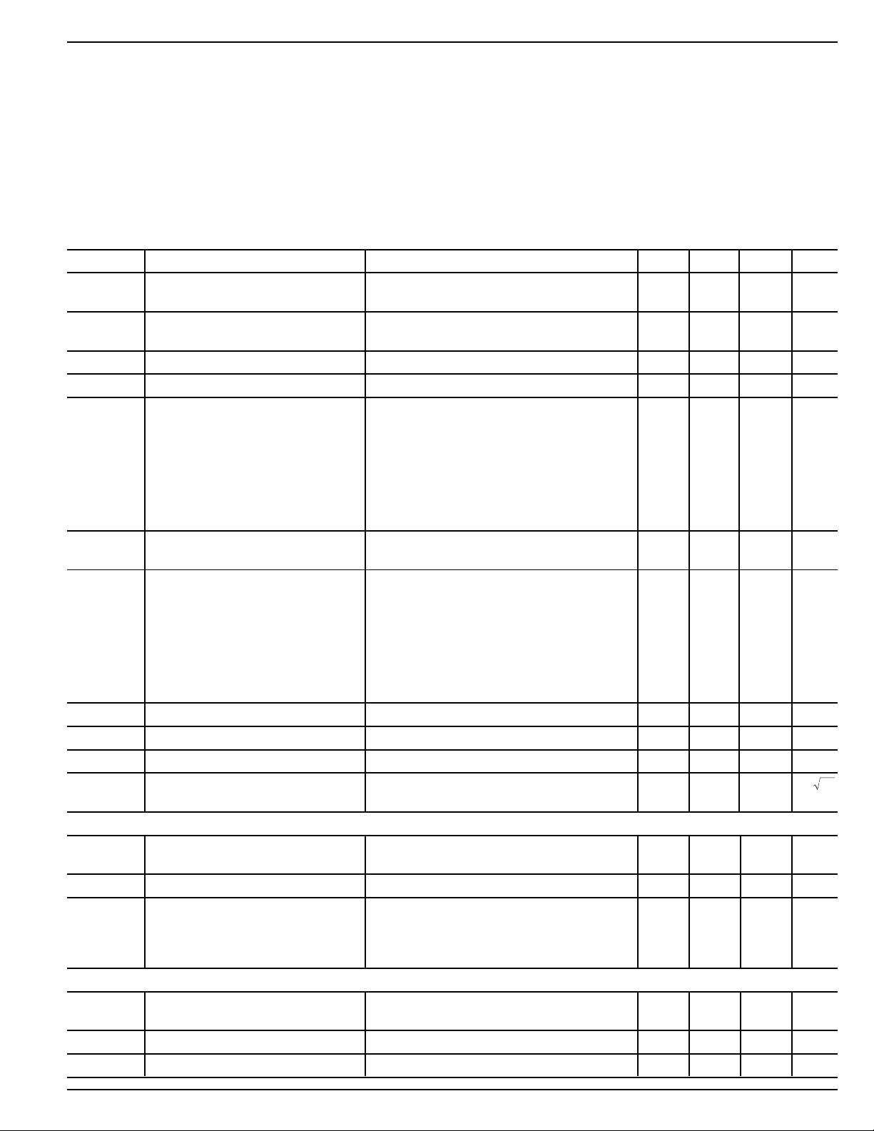
Electrical Characteristics
VIN = V
Symbol Parameter Conditions Min Typical Max Units
V
O
∆V
O
∆VO/V
∆VO/V
V
– V
IN
I
GND
I
GND
PSRR Ripple Rejection 75 dB
I
LIMIT
∆VO/∆P
e
no
Enable Input
V
IL
V
IH
I
IL
I
IH
Error Flag Output
V
ERR
V
OL
I
FL
+ 1V; IL = 100µA; CL = 1.0µF; VEN ≥ 2.0V; TJ = 25°C, bold values indicate –40°C ≤ TJ ≤ +125°C; unless noted.
OUT
Output Voltage Accuracy variation from nominal V
OUT
–11%
–22%
/∆T Output Voltage Note 4 40 ppm/°C
Temperature Coefficient
O
O
O
Line Regulation VIN = V
Load Regulation IL = 0.1mA to 150mA, Note 5 0.02 0.2 %
Dropout Voltage, Note 6 IL = 100µA1750mV
+ 1V to 16V 0.004 0.012 % / V
OUT
70 mV
IL = 50mA 110 150 mV
230 mV
= 100mA 140 250 mV
I
L
300 mV
IL = 150mA 165 275 mV
350 mV
Quiescent Current VEN ≤ 0.4V (shutdown) 0.01 1 µA
VEN ≤ 0.18V (shutdown) 5 µA
Ground Pin Current, Note 7 VEN ≥ 2.0V, IL = 100µA80125µA
150 µA
IL = 50mA 350 600 µA
800 µA
= 100mA 600 1000 µA
I
L
1500 µA
IL = 150mA 1300 1900 µA
2500 µA
Current Limit V
D
Thermal Regulation Note 8 0.05 %/W
Output Noise IL = 50mA, CL = 4.7µF, 470pF from BYP 260
= 0V 320 500 mA
OUT
nV Hz
to GND (MM package only)
Enable Input Logic-Low Voltage regulator shutdown 0.4 V
0.18 V
Enable Input Logic-High Voltage regulator enabled 2.0 V
Enable Input Current VIL ≤ 0.4V 0.01 –1 µA
≤ 0.18V –2 µA
V
IL
VIH ≥ 2.0V 5 20 µA
VIH ≥ 2.0V 25 µA
Flag Threshold undervoltage condition (below nominal) –2 –6 –10 %
Note 9
Output Logic-Low Voltage IL = 1mA, undervoltage condition 0.2 0.4 V
Flag Leakage Current flag off, V
= 0V to 16V –1 0.1 +1 µA
FLAG
IN
January 2000 3 MIC5206
Page 4
MIC5206 Micrel
Note 1: Exceeding the absolute maximum rating may damage the device.
Note 2. The device is not guaranteed to function outside its operating rating.
Note 3: The maximum allowable power dissipation at any T
allowable power dissipation will result in excessive die temperature, and the regulator will go into thermal shutdown. The θ
(ambient temperature) is P
A
MIC5205-x.xBM5 (all versions) is 220°C/W, and the MIC5206-x.xBMM (all versions) is 200°C/W, mounted on a PC board (see “Thermal
Considerations” for further details).
Note 4: Output voltage temperature coefficient is defined as the worst case voltage change divided by the total temperature range.
Note 5: Regulation is measured at constant junction temperature using low duty cycle pulse testing. Parts are tested for load regulation in the load
range from 0.1mA to 150mA. Changes in output voltage due to heating effects are covered by the thermal regulation specification.
Note 6: Dropout Voltage is defined as the input to output differential at which the output voltage drops 2% below its nominal value measured at 1V
differential.
Note 7: Ground pin current is the regulator quiescent current plus pass transistor base current. The total current drawn from the supply is the sum of
the load current plus the ground pin current.
Note 8: Thermal regulation is defined as the change in output voltage at a time “t” after a change in power dissipation is applied, excluding load or line
regulation effects. Specifications are for a 150mA load pulse at VIN = 16V for t = 10ms.
Note 9: The error flag comparator includes 3% hysteresis.
D(max)
= (T
– TA) ÷ θJA. Exceeding the maximum
J(max)
JA
of the
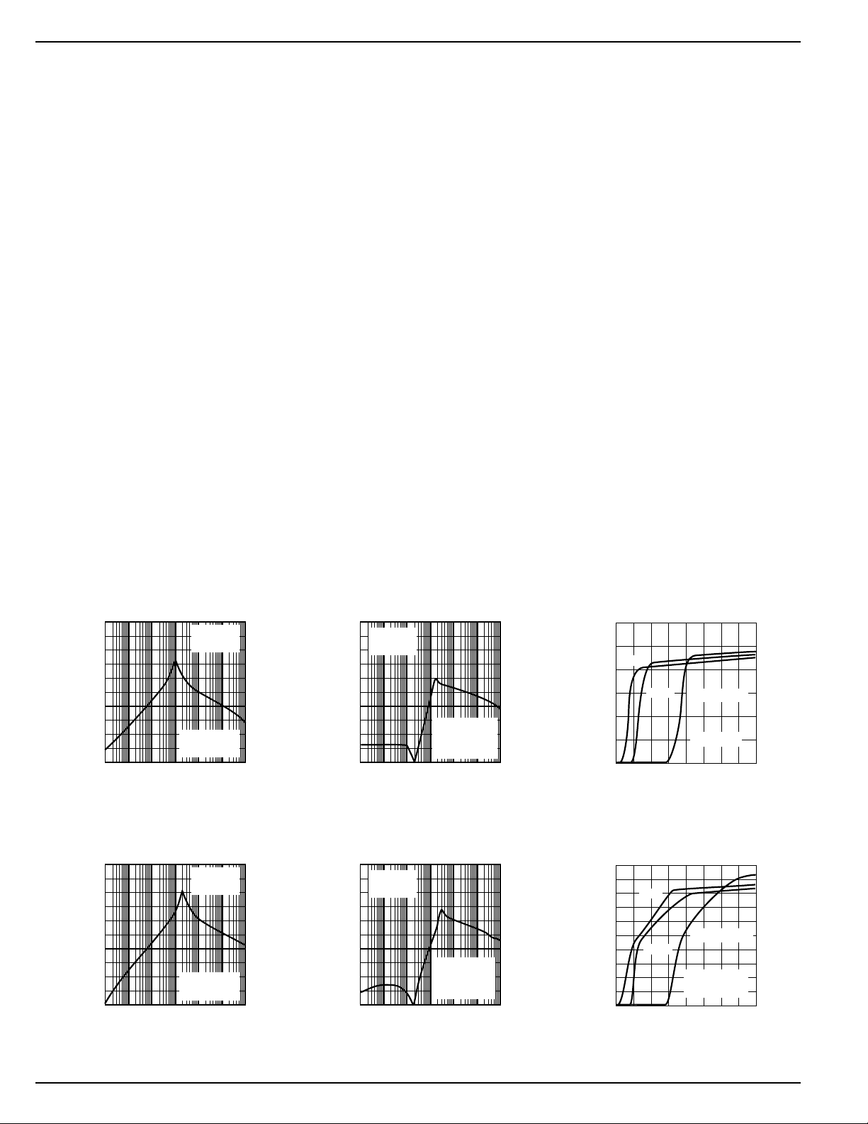
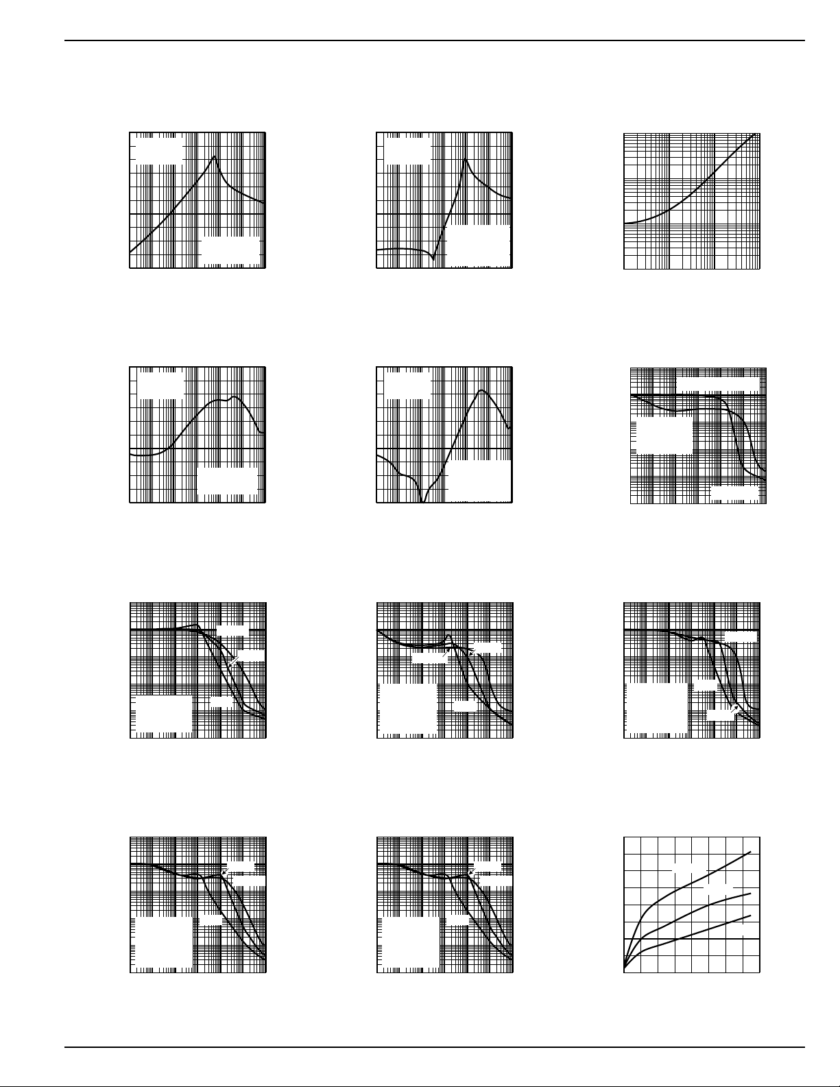
Typical Characteristics
Power Supply
Rejection Ratio
0
-20
-40
-60
PSRR (dB)
-80
-100
1E+11E+21E+31E+41E+51E+61E+7
10
1k
100
FREQUENCY (Hz)
Power Supply
Rejection Ratio
0
-20
-40
-60
PSRR (dB)
-80
-100
1E+11E+21E+31E+41E+51E+61E+7
10
1k
100
FREQUENCY (Hz)
10k
10k
I
C
I
C
OUT
OUT
100k
OUT
OUT
100k
VIN = 6V
V
= 5V
OUT
= 100µA
= 1µF
VIN = 6V
V
= 5V
OUT
= 1mA
= 1µF
1M
1M
10M
10M
Power Supply
Rejection Ratio
0
VIN = 6V
V
-20
-40
-60
PSRR (dB)
-80
-100
= 5V
OUT
I
= 100µA
OUT
C
= 2.2µF
OUT
C
= 0.01µF
BYP
1E+11E+21E+31E+41E+51E+61E+7
10
1k
100
10k
FREQUENCY (Hz)
100k
1M
Power Supply
Rejection Ratio
0
VIN = 6V
V
-20
-40
-60
PSRR (dB)
-80
-100
= 5V
OUT
I
= 1mA
OUT
C
= 2.2µF
OUT
C
= 0.01µF
BYP
1E+11E+21E+31E+41E+51E+61E+7
10
1k
100
10k
FREQUENCY (Hz)
100k
1M
10M
10M
Power Supply Ripple Rejection
vs. Voltage Drop
60
50
1mA
40
30
20
10
RIPPLE REJECTION (dB)
10mA
I
= 100mA
OUT
C
= 1µF
OUT
0
0 0.1 0.2 0.3 0.4
VOLTAGE DROP (V)
Power Supply Ripple Rejection
100
RIPPLE REJECTION (dB)
vs. Voltage Drop
90
80
1mA
70
60
50
40
10mA
30
20
10
0
0 0.1 0.2 0.3 0.4
VOLTAGE DROP (V)
I
C
OUT
C
BYP
= 100mA
OUT
= 2.2µF
= 0.01µF
MIC5206 4 January 2000
Page 5
MIC5206 Micrel
√
0.0001
0.001
0.01
0.1
1
10
1E+11E+21E+31E+41E+51E+6 1E+7
NOISE (µV/√Hz)
FREQUENCY (Hz)
√
√
0.0001
0.001
0.01
0.1
1
10
1E+11E+21E+31E+41E+51E+6 1E+7
NOISE (µV/√Hz)
FREQUENCY (Hz)
Typical Characteristics
Power Supply
Rejection Ratio
0
VIN = 6V
V
OUT
= 5V
-20
-40
-60
PSRR (dB)
-80
-100
1E+11E+21E+31E+41E+51E+61E+7
10
100
FREQUENCY (Hz)
I
= 10mA
OUT
C
= 1µF
OUT
1k
10k
100k
1M
Power Supply
Rejection Ratio
0
VIN = 6V
V
-20
-40
-60
PSRR (dB)
-80
-100
= 5V
OUT
I
= 100mA
OUT
C
= 1µF
OUT
1E+11E+21E+31E+41E+51E+61E+7
10
1k
100
10k
FREQUENCY (Hz)
100k
1M
10M
10M
Power Supply
Rejection Ratio
0
VIN = 6V
V
OUT
= 5V
-20
-40
-60
PSRR (dB)
-80
-100
1E+11E+21E+31E+41E+51E+61E+7
10
100
FREQUENCY (Hz)
I
= 10mA
OUT
C
= 2.2µF
OUT
C
= 0.01µF
BYP
1k
10k
100k
1M
Power Supply
Rejection Ratio
0
VIN = 6V
V
-20
-40
-60
PSRR (dB)
-80
-100
= 5V
OUT
I
= 100mA
OUT
C
= 2.2µF
OUT
C
= 0.01µF
BYP
1E+11E+21E+31E+41E+51E+61E+7
10
1k
100
10k
FREQUENCY (Hz)
100k
1M
10M
10M
Turn-On Time
vs. Bypass Capacitance
10000
1000
TIME (µs)
100
10
10 100 1000 10000
CAPACITANCE (pF)
Noise Performance
10
1
0.1
0.01
NOISE (µV/√Hz)
0.001
0.0001
1E+11E+21E+31E+41E+51E+61E+7
10
10mA, C
1mA
C
= 1µF
OUT
C
= 10nF
BYP
1k
100
FREQUENCY (Hz)
10k 100k 1M 10M
OUT
V
OUT
= 1µF
= 5V
Noise Performance
10
Hz)
1
0.1
100mA
0.01
NOISE (µV/
V
= 5V
OUT
0.001
C
= 10µF
OUT
electrolytic
0.0001
1E+11E+21E+31E+41E+51E+6 1E+7
10
100
FREQUENCY (Hz)
1mA
1k
10k 100k1M10M
10mA
Noise Performance
100mA
V
= 5V
OUT
C
= 22µF
OUT
tantalum
C
= 10nF
BYP
100
1k
10
10mA
1mA
10k 100k1M10M
Noise Performance
10
1
Hz)
0.1
0.01
V
= 5V
NOISE (µV/
0.0001
OUT
C
= 10µF
OUT
0.001
electrolytic
C
= 100pF
BYP
1E+11E+21E+31E+41E+51E+6 1E+7
10
100
FREQUENCY (Hz)
1mA
10mA
1k
10k 100k1M10M
100mA
Dropout Voltage
Noise Performance
10
1
Hz)
0.1
0.01
V
NOISE (µV/
0.001
0.0001
= 5V
OUT
C
= 10µF
OUT
electrolytic
C
= 1nF
BYP
1E+11E+21E+31E+41E+51E+6 1E+7
10
1k
100
FREQUENCY (Hz)
10mA
100mA
1mA
10k 100k1M10M
Noise Performance
V
= 5V
OUT
C
= 10µF
OUT
electrolytic
C
= 1nF
BYP
100
1k
10
10mA
100mA
1mA
DROPOUT VOLTAGE (mV)
10k 100k1M10M
vs. Output Current
320
280
240
200
+125°C
+25°C
160
120
80
40
0
0 40 80 120 160
OUTPUT CURRENT (mA)
–40°C
January 2000 5 MIC5206
Page 6
MIC5206 Micrel
Applications Information
Enable/Shutdown
Forcing EN (enable/shutdown) high (> 2V) enables the regulator. EN is compatible with CMOS logic gates.
If the enable/shutdown feature is not required, connect EN
(enable) to IN (supply input). Refer to the text with Figures 1a
and 2.
Input Capacitor
A 1µF capacitor should be placed from IN to GND if there is
more than 10 inches of wire between the input and the ac filter
capacitor or if a battery is used as the input.
Reference Bypass Capacitor
BYP (reference bypass) is connected to the internal voltage
reference. A 470pF capacitor (C
GND quiets this reference, providing a significant reduction in
output noise. See Figure 2. C
margin; when using C
BYP
, output capacitors of 2.2µF or
BYP
greater are generally required to maintain stability.
The start-up speed of the MIC5206 is inversely proportional
to the size of the reference bypass capacitor. Applications
requiring a slow ramp-up of output voltage should consider
larger values of C
consider omitting C
. Likewise, if rapid turn-on is necessary,
BYP
.
BYP
If output noise is not a major concern, omit C
BYP open.
Output Capacitor
An output capacitor is required between OUT and GND to
prevent oscillation. The minimum size of the output capacitor
is dependent upon whether a reference bypass capacitor is
used. 1.0µF minimum is recommended when C
used (see Figure 2). 2.2µF minimum is recommended when
C
is 470pF (see Figure 2). Larger values improve the
BYP
regulator’s transient response. The output capacitor value
may be increased without limit.
The output capacitor should have an ESR (effective series
resistance) of about 5Ω or less and a resonant frequency
above 1MHz. Most tantalum or aluminum electrolytic capacitors are adequate; film types will work, but are more expensive. Since many aluminum electrolytics have electrolytes
that freeze at about –30°C, solid tantalums are recommended for operation below –25°C.
At lower values of output current, less output capacitance is
required for output stability. The capacitor can be reduced to
0.47µF for current below 10mA or 0.33µF for currents below
1mA.
No-Load Stability
The MIC5205 will remain stable and in regulation with no load
(other than the internal voltage divider) unlike many other
voltage regulators. This is especially important in CMOS
RAM keep-alive applications.
Error Flag Ouput
The error flag is an open-collector output and is active (low)
when an undervoltage of approximately 5% below the nominal output voltage is detected. A pullup resistor from IN to
FLAG is shown in all schematics.
) connected from BYP to
BYP
reduces the regulator phase
and leave
BYP
is not
BYP
If an error indication is not required, FLAG may be left open
and the pullup resistor may be omitted.
Enable Pin Ramp and the Error Flag
To prevent indeterminate behavior on the error flag during
power down of the device, ensure that the fall time of the
enable pin signal, from logic high to logic low, is faster than
100µs.
Fixed Regulator Applications
MIC5206-x.xBM5
V
IN
EN (pin 3) may be
connected directly
to IN (pin 1).
15
2
34
100k
Error Flag
V
OUT
C
OUT
1µF
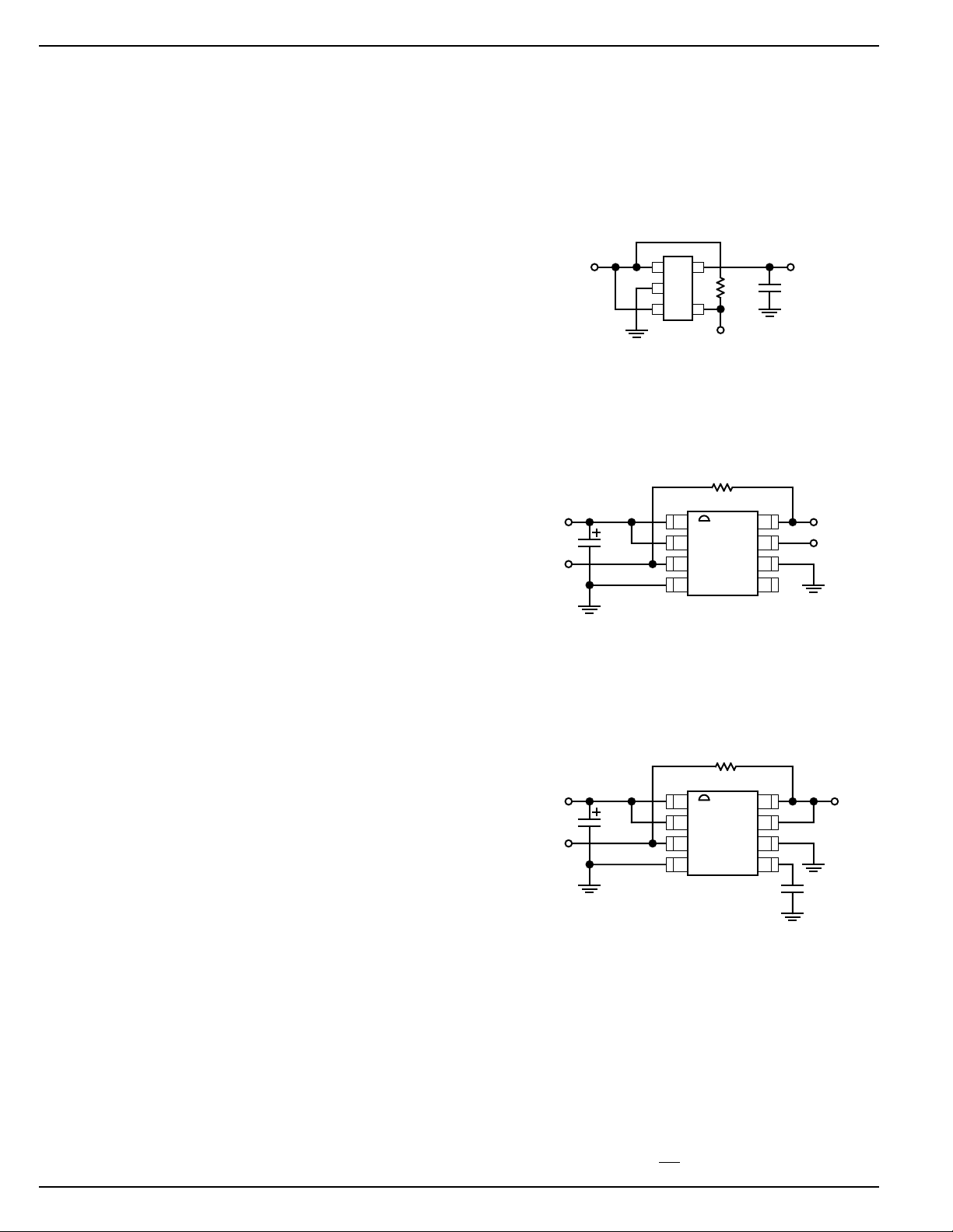
Figure 1a. Low-Noise Fixed Voltage Application
EN (pin 3) is shown connected to IN (pin 1) for an application
where enable/shutdown is not required. The error flag is
shown with a 100kΩ pullup resistor.
V
OUT
Flag Output
(optional)
1µF
1
47k
2
3
4
MIC5206-x.xBMM
8
V
7
6
5
IN
Enable
Figure 1b. Low-Noise Fixed Voltage Application
Figure 1b is an example of a basic configuration where the
lowest-noise operation is not required. C
= 1µF minimum.
OUT
The error flag is shown with a 47kΩ pullup resistor.
Ultra-Low-Noise Application
V
OUT
Flag Output
(optional)
2.2µF
1
2
3
4
MIC5206-x.xBMM
47k
BYP
8
7
6
5
C
BYP
470pF
V
IN
Figure 2. Ultra-Low-Noise Fixed Voltage Application
Figure 2 includes a 470pF capacitor for low-noise operation
and shows EN (pin 7) connected to IN (pin 8) for an application where enable/shutdown is not required. The error flag is
shown with a 47kΩ pullup resistor.
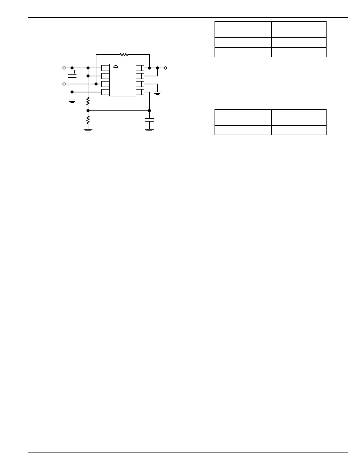
Adjustable Regulator Applications
Figure 3 shows the MIC5206BMM adjustable output voltage
configuration. Two resistors set the output voltage. The
formula for output voltage is:
R2
V = 1.242V
OUT
×+
R1
1
MIC5206 6 January 2000
Page 7
MIC5206 Micrel
Resistor values are not critical because ADJ (adjust) has a
high input impedance, but for best results use resistors of
470kΩ or less. A capacitor from ADJ to ground provides
greatly improved noise performance.
V
OUT
Flag Output
(optional)
2.2µF
1
2
3
4
R1
R2
47k
ADJ
MIC5206BMM
8
7
6
5
C
BYP
470pF
V
IN
Figure 3. Ultra-Low-Noise
Adjustable Voltage Application
Figure 3 also includes a 470pF capacitor for lowest-noise
operation and shows EN (pin 7) connected to IN (pin 8) for an
application where enable/shutdown is not required. C
OUT
=
2.2µF minimum. The error flag is shown with a 47kΩ pullup
resistor.
Thermal Considerations
Layout
The MIC5206-x.xBM5 (5-lead SOT-23 package) has the
following thermal characteristics when mounted on a single
layer copper-clad printed circuit board.
Multilayer boards having a ground plane, wide traces near the
pads, and large supply bus lines provide better thermal
conductivity.
PC Board
Dielectric
θθ
θ
θθ
JA
FR4 220°C/W
Ceramic 200°C/W
SOT-23-5 Thermal Characteristics
The “worst case” value of 220°C/W assumes no ground
plane, minimum trace widths, and a FR4 material board.
The MIC5206-xxBMM (8-lead MSOP) has a thermal resistance of 200°C/W when mounted on a FR4 board with
minimum trace widths and no ground plane.
PC Board
Dielectric
FR4 200°C
θθ
θ
θθ
JA
MSOP Thermal Characteristics
Nominal Power Dissipation and Die Temperature
The MIC5206-x.xBM5 at a 25°C ambient temperature will
operate reliably at over 450mW power dissipation when
mounted in the “worst case” manner described above. At an
ambient temperature of 40°C, the device may safely dissipate over 380mW. These power levels are equivalent to a die
temperature of 125°C, the maximum operating junction temperature for the MIC5206.
For additional heat sink characteristics, please refer to Micrel
Application Hint 17, “Calculating P.C. Board Heat Sink Area
For Surface Mount Packages”.
January 2000 7 MIC5206
Page 8
MIC5206 Micrel
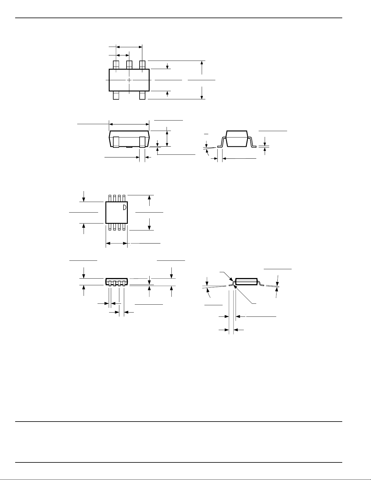
Package Information
1.90 (0.075) REF
0.95 (0.037) REF
3.02 (0.119)
2.80 (0.110)
0.122 (3.10)
0.112 (2.84)
0.50 (0.020)
0.35 (0.014)
1.75 (0.069)
1.50 (0.059)
1.30 (0.051)
0.90 (0.035)
0.199 (5.05)
0.187 (4.74)
0.120 (3.05)
0.116 (2.95)
3.00 (0.118)
2.60 (0.102)
0.15 (0.006)
0.00 (0.000)
SOT-23-5 (M5)
10°
0°
DIMENSIONS:
MM (INCH)
0.20 (0.008)
0.09 (0.004)
0.60 (0.024)
0.10 (0.004)
DIMENSIONS:
INCH (MM)
0.036 (0.90)
0.032 (0.81)
0.012 (0.03)
0.0256 (0.65) TYP
0.008 (0.20)
0.004 (0.10)
0.043 (1.09)
0.038 (0.97)
0.012 (0.30) R
5° MAX
0° MIN
0.007 (0.18)
0.005 (0.13)
0.012 (0.03) R
0.039 (0.99)
0.035 (0.89)
0.021 (0.53)
8-Lead MSOP (MM)
MICREL INC. 1849 FORTUNE DRIVE SAN JOSE, CA 95131 USA
TEL + 1 (408) 944-0800 FAX + 1 (408) 944-0970 WEB http://www.micrel.com
This information is believed to be accurate and reliable, however no responsibility is assumed by Micrel for its use nor for any infringement of patents or
other rights of third parties resulting from its use. No license is granted by implication or otherwise under any patent or patent right of Micrel Inc.
© 2000 Micrel Incorporated
MIC5206 8 January 2000
 Loading...