

Page 1
MIC5012 Micrel
MIC5012
Dual High- or Low-Side MOSFET Driver
Not Recommended for New Designs
General Description
The MIC5012 is the dual member of the Micrel MIC501X
driver family. These ICs are designed to drive the gate of an
N-channel power MOSFET above the supply rail in highside power switch applications. The 14-pin MIC5012 is
extremely easy to use, requiring only a power FET and
nominal supply decoupling to implement either a high- or
low-side switch.
The MIC5012 charges a 1nF load in 60µs typical. Operation
down to 4.75V allows the MIC5012 to drive standard
MOSFETs in 5V low-side applications by boosting the gate
voltage above the logic supply. In addition, multiple, paralleled MOSFETs can be driven by a single MIC5012 for ultrahigh current applications.
Features
• 4.75V to 32V operation
• 2 independent drivers; implements high and low side
drivers
• Less than 1µA standby current in the “off” state per
channel
• Available in small outline SOIC packages
• Internal charge pump to drive the gate of an N-channel
power FET above supply
• Internal zener clamp for gate protection
• Minimum external parts count
• Can be used to boost drive to low-side power FETs
operating on logic supplies
• Independent supply pins for half-bridge applications
Other members of the Micrel driver family include the
MIC5010 full-featured driver, MIC5011 minimum parts count
driver, and MIC5013 protected 8-pin driver.
Applications
• Lamp drivers
• Motion Control
• Heater switching
For new designs, Micrel recommends the pin-compatible
MIC5016 dual MOSFET driver.
• Power bus switching
• Half or full H-bridge drivers
Typical Applications Ordering Information
ON
10µF
Control Input
OFF
ON
Control Input
OFF
+
1/2 MIC5012
V+
Input
Source
Gnd
Gate
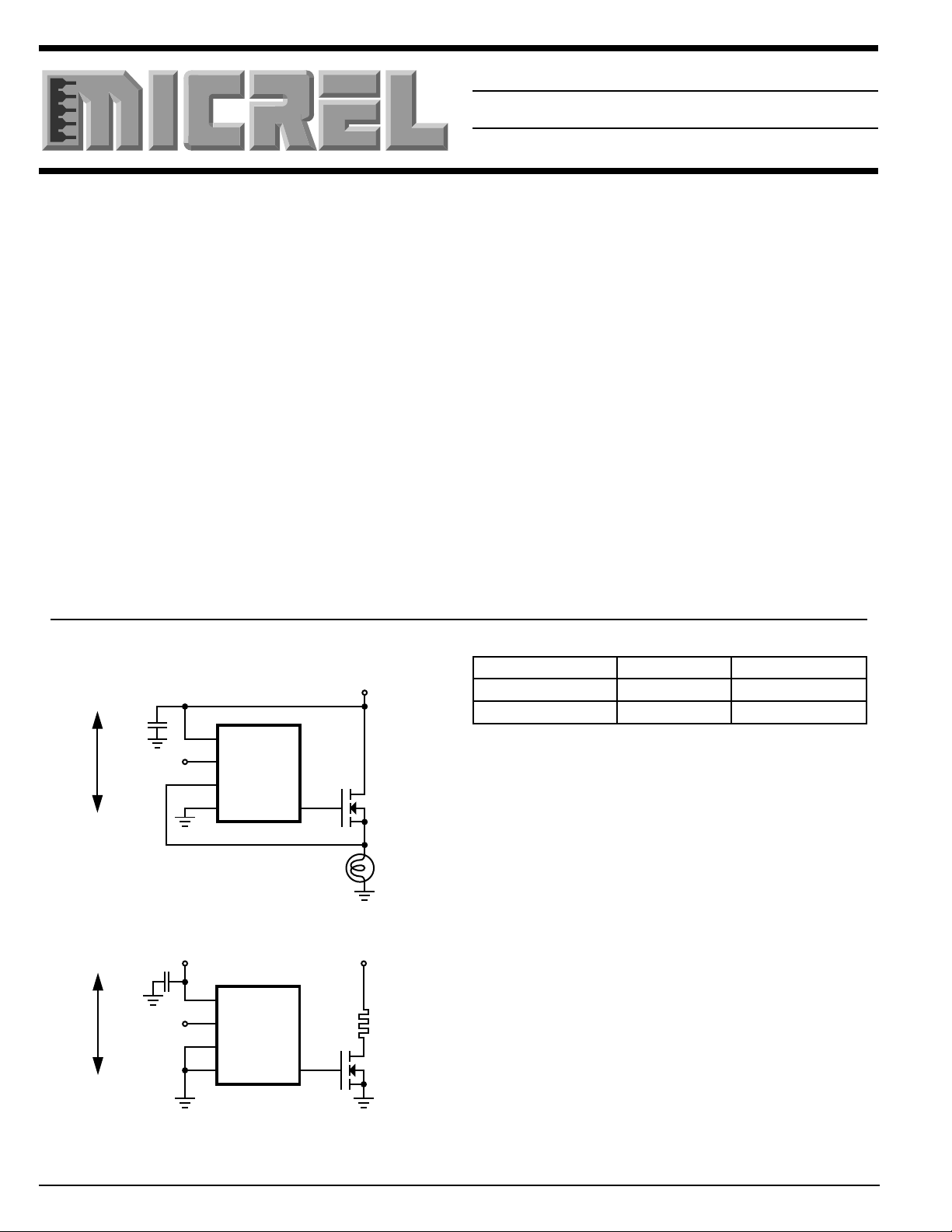
Figure 1. High Side Driver
10µF
+
1/2 MIC5012
V+
Input
Source
Gnd
Gate
14.4V
48V5V
IRF531
#6014
100W
Heater
IRF530
Part Number Temp. Range Package
MIC5012BN –40°C to +85°C 14-pin Plastic DIP
MIC5012BWM –40°C to +85°C 16-pin Wide SOIC
Note: The MIC5012 is ESD sensitive.
Figure 2. Low Side Driver
Protected under one or more of the following Micrel patents:
patent #4,951,101; patent #4,914,546
5-114 April 1998
Page 2
MIC5012 Micrel
34567
A
34567
A
8
Absolute Maximum Ratings (Note 1, 2)
Supply Voltage (V+), Pins 10, 12 –0.5V to 36V
Input Voltage, Pins 11, 14 –10V to V
Source Voltage, Pins 2, 5 –10V to V
Current into Pins 2, 5 50mA
Gate Voltage, Pins 4, 6 –1V to 50V
Junction Temperature 150°C
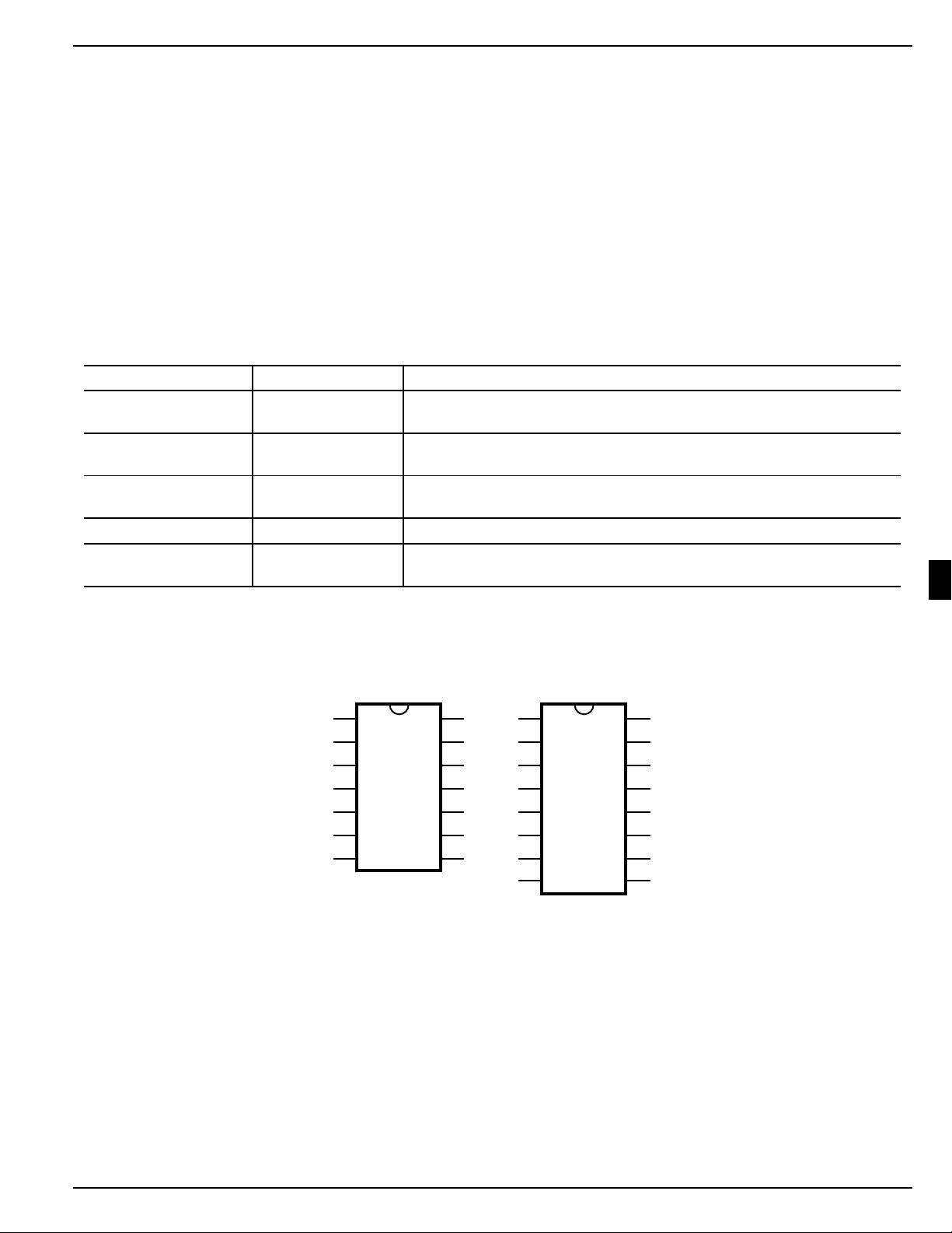
Pin Description (Refer to Typical Applications)
DIP Pin Number Pin Name Pin Function
12, 10 V
14, 11 Input Turns on power MOSFET when taken above threshold (3.5V typical).
2, 5 Source Connects to source lead of power FET and is the return for the gate clamp
3 Ground
4, 6 Gate Drives and clamps the gate of the power FET. Clamped to approximately –
+
Supply; must be decoupled to isolate from large transients caused by the
power FET drain. 10µF is recommended close to pins 1 and 4.
Requires <1 µA to switch.
zener. Can safely swing to –10V when turning off inductive loads.
0.7V by an internal diode when turning off inductive loads.
Operating Ratings (Notes 1, 2)
Power Dissipation 1.56W
+
θJA (Plastic DIP) 80 °C/W
+
θJA (SOIC) 105°C/W
Ambient Temperature: B version –40°C to +85°C
Storage Temperature –65°C to +150°C
Lead Temperature 260°C
(Soldering, 10 seconds)
Supply Voltage (V+), Pin 1 4.75V to 32V high side
4.75V to 15V low side
5
Pin Configuration
MIC5012 (N, J)
1
2
Input A
NC
Source A
Gnd
Source B V+ B
Gate B
NC
V+
Input BGate A
NC
NC
NC
14
13
12
11
10
MIC5012 (WM)
1
NC
2
Source A
Gnd
Source B V+ B
9
8
Gate B
NC
NC
Input A
NC
V+
Input BGate A
NC
NC
NC
16
15
14
13
12
11
10
9
April 1998 5-115
Page 3
MIC5012 Micrel
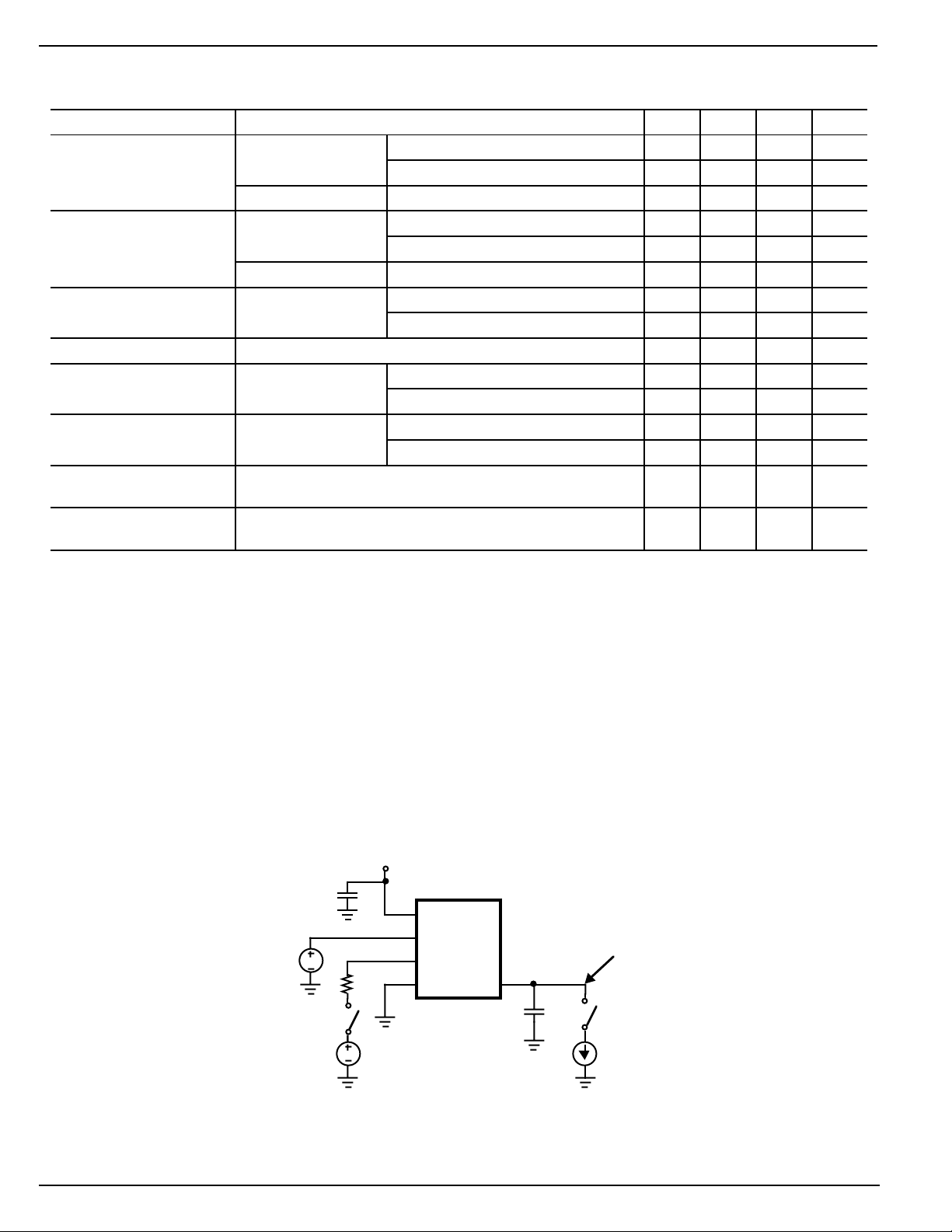
Electrical Characteristics (Note 3) Test circuit. T
= –55°C to +125°C, V+ = 15V, all switches open, unless
A
otherwise specified.
Parameter Conditions Min Typical Max Units
Supply Current V+ = 32V VIN = 0V, S2 closed 0.1 10 µA
(per section) VIN = VS = 32V 8 20 mA
V+ = 5V VIN = 5V, S2 closed 1.6 4 mA
Logic Input Voltage V+ = 4.75V Adjust VIN for V
Adjust VIN for V
V+ = 15V Adjust VIN for V
Logic Input Current, I
2
V+ = 32V VIN = 0V –1 µA
VIN = 32V 1 µA
Input Capacitance Pins 11, 14 5 pF
Gate Drive, V
GATE
S1, S2 closed, V+ = 4.75V, I
VS = V+, VIN = 5V V+ = 15V, I
GATE
GATE
Zener Clamp, S2 closed, VIN = 5V V+ = 15V, VS = 15V 11 12.5 15 V
V
– V
GATE
Gate Turn-on Time, t
(Note 4) for V
Gate Turn-off Time, t
Note 1 Absolute Maximum Ratings indicate limits beyond which damage to the device may occur. Electrical specifications do not apply when
Note 2 The MIC5012 is ESD sensitive.
Note 3 Minimum and maximum Electrical Characteristics are 100% tested at TA = 25°C and TA = 85°C, and 100% guaranteed over the entire
Note 4 Test conditions reflect worst case high-side driver performance. Low-side and bootstrapped topologies are significantly faster—see
SOURCE
ON
OFF
operating the device beyond its specified Operating Ratings.
range. Typicals are characterized at 25°C and represent the most likely parametric norm.
Applications Information. Maximum value of switching speed seen at 125°C, units operated at room temperature will reflect the typical
values shown.
VIN switched from 0 to 5V; measure time 60 200 µs
to reach 20V
GATE
VIN switched from 5 to 0V; measure time 4 10 µs
for V
to reach 1V
GATE
V+ = 32V, VS = 32V 11 13 16 V
low 2 V
GATE
high 4.5 V
GATE
high 5.0 V
GATE
= 0, VIN = 4.5V 7 10 V
= 100µA, VIN = 5V 24 27 V
Test Circuit
V+
+
1µF
V
IN
500Ω
1W
S2
VS
1/2 MIC5012
V+
Input
Source
Gnd
Gate
1nF
S1
I
V
GATE
GATE
5-116 April 1998
Page 4
MIC5012 Micrel
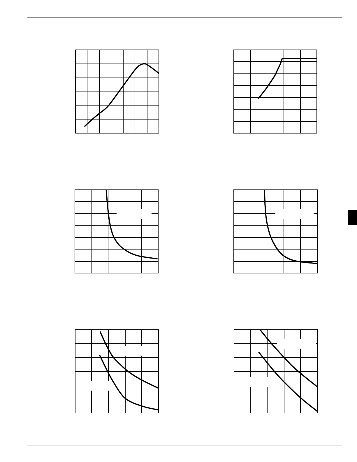
Typical Characteristics (Continued)
DC Gate Voltage
Supply Current
12
above Supply
14
10
8
6
4
2
SUPPLY CURRENT (mA)
0
0 5 10 15 20 25 30 35
SUPPLY VOLTAGE (V)
High-side Turn-on Time*
350
300
250
200
C =1 nF
GATE
12
10
8
6
VGATE – V+ (V)
4
2
0
0 3 6 9 12 15
SUPPLY VOLTAGE (V)
High-side Turn-on Time*
3.5
3.0
C =10 nF
2.5
2.0
GATE
5
150
100
TURN-ON TIME (µS)
50
0
03691215
SUPPLY VOLTAGE (V)
Low-side Turn-on Time
for Gate = 5V
1000
TURN-ON TIME (µS)
300
100
30
10
3
C =1 nF
GATE
C =10 nF
GATE
1.5
1.0
TURN-ON TIME (mS)
0.5
0
03691215
SUPPLY VOLTAGE (V)
Low-side Turn-on Time
for Gate = 10V
3000
C =10 nF
1000
TURN-ON TIME (µS)
300
100
30
10
C =1 nF
GATE
GATE
1
03691215
SUPPLY VOLTAGE (V)
* Time for gate to reach V+ + 5V in test circuit with VS = V+ – 5V.
April 1998 5-117
3
03691215
SUPPLY VOLTAGE (V)
Page 5
MIC5012 Micrel
Typical Characteristics (Continued)
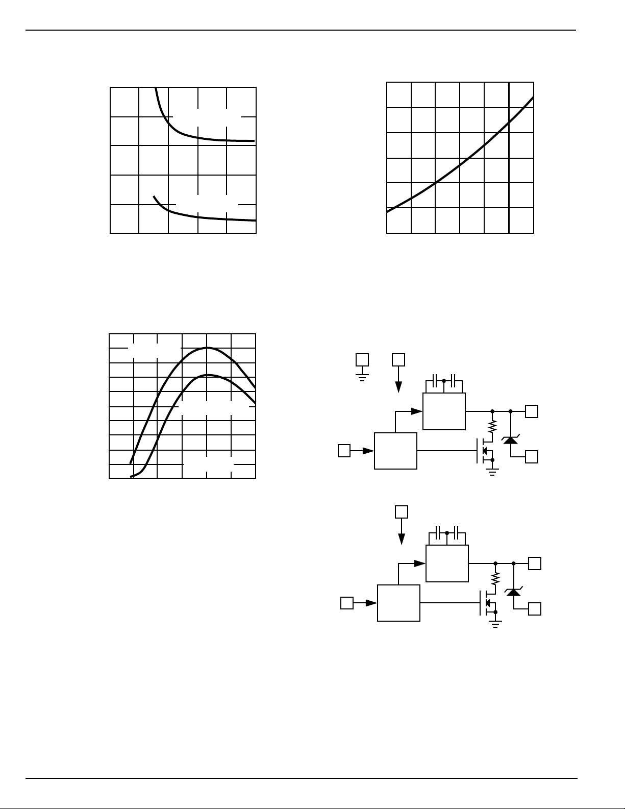
Turn-off Time
50
40
30
20
TURN-OFF TIME (µS)
10
0
03691215
C =10 nF
GATE
C =1 nF
GATE
SUPPLY VOLTAGE (V)
Charge Pump
Output Current
250
+
200
V =V
GATE
Turn-on Time
2.0
1.75
1.5
1.25
1.0
0.75
NORMALIZED TURN-ON TIME
0.5
–25 0 25 50 75 100 125
Block Diagram
Ground
312
V+
DIE TEMPERATURE (°C)
MIC5012
150
V =V +5V
GATE
100
50
VS=V –5V
CHARGE-PUMP CURRENT (µA)
0
0 5 10 15 20 25 30
+
+
SUPPLY VOLTAGE (V)
Applications Information
Functional Description (Refer to Block Diagram)
The MIC5012 consists of two independent drivers sharing
a common ground. The functions are controlled via a logic
block connected to the logic input. When the input is low, all
functions are turned off for low standby current and the gate
of the power MOSFET is also held low through 500Ω to an
N-channel switch. When the input is taken above the turnon threshold (3.5V typical), the N-channel switch turns off
and the charge pump is turned on to charge the gate of the
power FET.
The charge pump incorporates a 100kHz oscillator and onchip pump capacitors capable of charging 1nF to 5V above
supply in 60µs typical. The charge pump is capable of
pumping the gate up to over twice the supply voltage. For
this reason, a zener clamp (12.5V typical) is provided
between the gate pin and source pin to prevent exceeding
Input
Input
14
11
CHARGE
PUMP
500Ω
LOGIC
V+
10
CHARGE
PUMP
500Ω
LOGIC
4
12.5V
2
6
12.5V
5
Gate
Source
Gate
Source
the VGS rating of the MOSFET at high supplies.
Since the supply pins are independent, the two drivers
contained in the MIC5012 can be operated from separate
supplies of different values (see Figure 6).
Construction Hints
High current pulse circuits demand equipment and assembly techniques that are more stringent than normal, low
current lab practices. The following are the sources of
5-118 April 1998
Page 6
MIC5012 Micrel
Input
Source
Gate
1/2 MIC5012
V+
Gnd
IRFP044 (2)
10µF
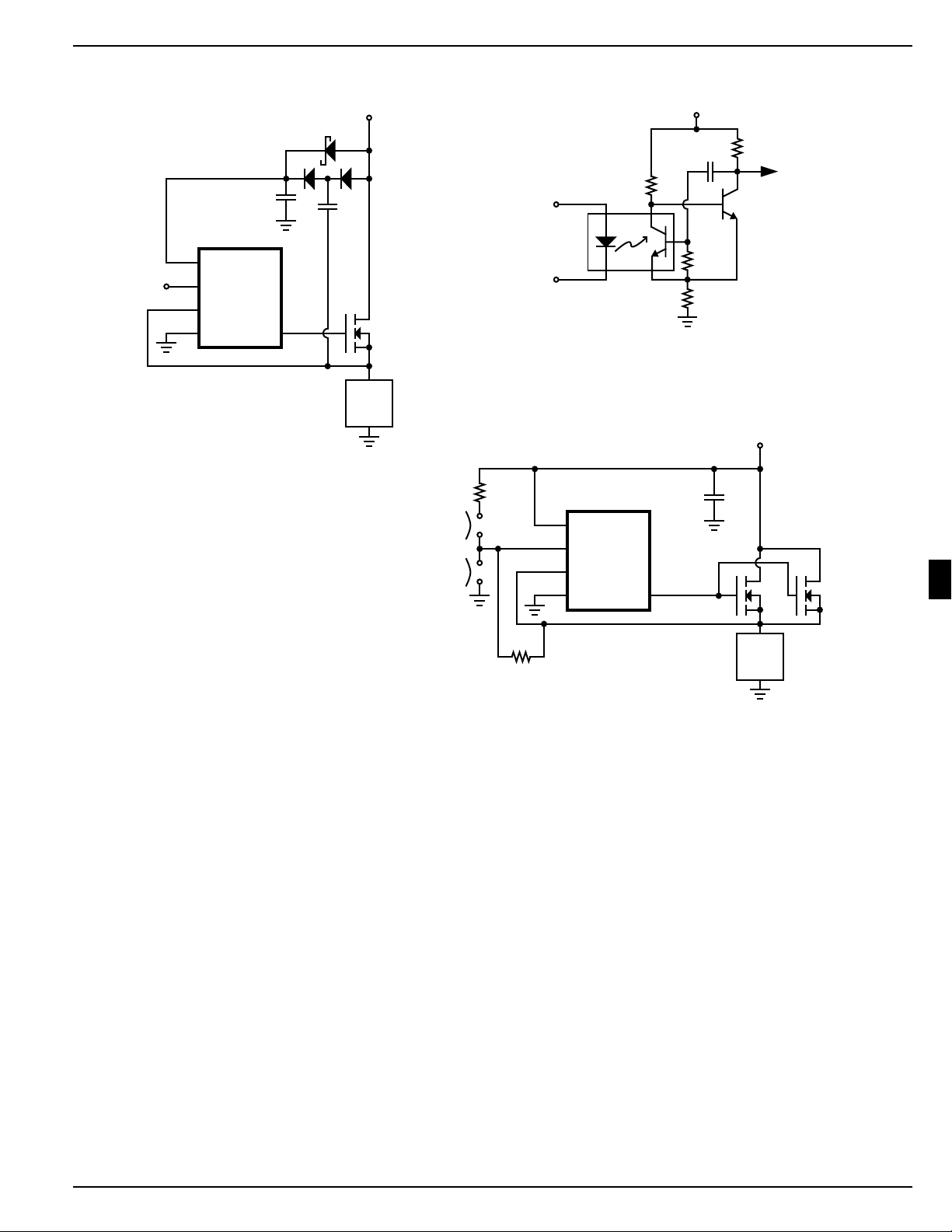
Figure 5. 50-Ampere
Industrial Switch
+
LOAD
24V
330kΩ
100kΩ
OFF
ON
CR2943-NA102A
(GE)
Applications Information (Continued)
Control Input
1N5817
100nF
1/2 MIC5012
V+
Input
Source
Gnd
Gate
+
Figure 3. Bootstrapped
High-Side Driver
7 to 15V
10µF
LOAD
1N4001 (2)
IRF540
10mA
Control Input
15V
33pF
100kΩ
4N35
100kΩ
1kΩ
33kΩ
To MIC5012
MPSA05
Figure 4. Improved
Opto-Isolator Performance
Input
pitfalls most often encountered during prototyping: Supplies: many bench power supplies have poor transient
response. Circuits that are being pulse tested, or those that
operate by pulse-width modulation will produce strange
results when used with a supply that has poor ripple
rejection, or a peaked transient response. Always monitor
the power supply voltage that appears at the drain of a highside driver (or the supply side of the load in a low-side driver)
with an oscilloscope. It is not uncommon to find bench
power supplies in the 1kW class that overshoot or undershoot by as much as 50% when pulse loaded. Not only will
the load current and voltage measurements be affected, but
it is possible to over-stress various components—especially electrolytic capacitors—with possibly catastrophic
results. A 10µF supply bypass capacitor at the chip is
recommended.
Residual Resistances:
may also cause confusing results. For example, a circuit
may employ a 50mΩ power MOSFET for low drop, but
careless construction techniques could easily add 50 to
100mΩ resistance. Do not use a socket for the MOSFET. If
the MOSFET is a TO-220 type package, make high-current
drain connections to the tab. Wiring losses have a profound
effect on high-current circuits. A floating millivoltmeter can
identify connections that are contributing excess drop under load.
Resistances in circuit connections
Circuit Topologies
The MIC5012 is suited for use with standard MOSFETs in
high- or low-side driver applications. In addition, the MIC5012
works well in applications where, for faster switching times,
the supply is bootstrapped from the MOSFET source output. Low voltage, high-side drivers (such as shown in Figure
1) are the slowest; their speed is reflected in the gate turnon time specifications. The fastest drivers are the low-side
and bootstrapped high-side types (Figures 2 and 4). Load
current switching times are often much faster than the time
to full gate enhancement, depending on the circuit type, the
MOSFET, and the load. Turn-off times are essentially the
same for all circuits (less than 10µs to VGS = 1V). The choice
of one topology over another is based on a combination of
considerations including speed, voltage, and desired system characteristics.
High-Side Driver (Figure 1). The high-side topology works
well down to V+ = 7V with standard MOSFETs. From 4.75
to 7V supply, a logic-level MOSFET can be substituted
since the MIC5012 will not reach 10V gate enhancement
(10V is the maximum rating for logic-compatible MOSFETs).
5
April 1998 5-119
Page 7
MIC5012 Micrel
Applications Information (Continued)
High-side drivers implemented with MIC501X drivers are
self-protected against inductive switching transients. During turn-off an inductive load will force the MOSFET source
5V or more below ground, while the MIC5012 holds the gate
at ground potential. The MOSFET is forced into conduction,
and it dissipates the energy stored in the load inductance.
The MIC5012 source pin is designed to withstand this
negative excursion without damage. External clamp diodes
are unnecessary.
Low-Side Driver (Figure 2). A key advantage of the lowside topology is that the load supply is limited only by the
MOSFET BV
protect the MOSFET drain terminal from inductive switching transients. The MIC5012 supply should be limited to
15V in low-side topologies; otherwise, a large current will be
forced through the gate clamp zener. The switching speed
to 10V enhancement is 300µs driving 1nF on a 5V supply.
On a 15V supply the turn-on time is less than 2µs to 10V
Low-side drivers constructed with the MIC501X family are
also fast; the MOSFET gate is driven to near supply
immediately when commanded ON. Typical circuits achieve
10V enhancement in 10µs or less on a 12 to 15V supply.
Modifying Switching Times. Do not add external capacitors
to the MOSFET gate. Add a resistor (1kΩ to 51kΩ) in series
with the gate to slow down the switching time.
Bootstrapped High-Side Driver (Figure 3). The speed of
a high-side driver can be increased to better than 10µs by
bootstrapping the supply off of the MOSFET source. This
topology can be used where the load is pulse-width modulated (100Hz to 20kHz), or where it is energized continu-
rating. Clamping may be required to
DSS
ously. The Schottky barrier diode prevents the MIC5012
supply pin from dropping more than 200mV below the drain
supply, and it also improves turn-on time on supplies of less
than 10V. Since the supply current in the “off” state is only
a small leakage, the 100nF bypass capacitor tends to
remain charged for several seconds after the MIC5012 is
turned off. In a PWM application the chip supply is sustained
at a higher potential than the system supply, which improves switching time.
Opto-Isolated Interface (Figure 4). Although the MIC5012
has no special input slew rate requirement, the lethargic
transitions provided by an opto-isolator may cause oscillations on the rise and fall of the output. The circuit shown
accelerates the input transitions from a 4N35 opto-isolator
by adding hysteresis. Opto-isolators are used where the
control circuitry cannot share a common ground with the
MIC5012 and high-current power supply, or where the
control circuitry is located remotely. This implementation is
intrinsically safe; if the control line is severed the MIC5012
will turn OFF.
Industrial Switch (Figure 5). The most common manual
control for industrial loads is a push button on/off switch.
The “on” button is physically arranged in a recess so that in
a panic situation the “off” button, which extends out from the
control box, is more easily pressed. This circuit is compatible with control boxes such as the CR2943 series (GE).
The circuit is configured so that if both switches close
simultaneously, the “off” button has precedence.
This application also illustrates how two (or more) MOSFETs
PWM
INPUT
1N4148
22kΩ
22kΩ
2N3904
220pF
15V
1nF
10kΩ
1/2 MIC5012
V+
Input
Source
Gate
+
10µF
1/2 MIC5012
V+
Input
Source
Gnd
Gate
100nF
1N5817
+
1µF
15V
1N4001 (2)
IRF541
IRF541
12V,
M
10A Stalled
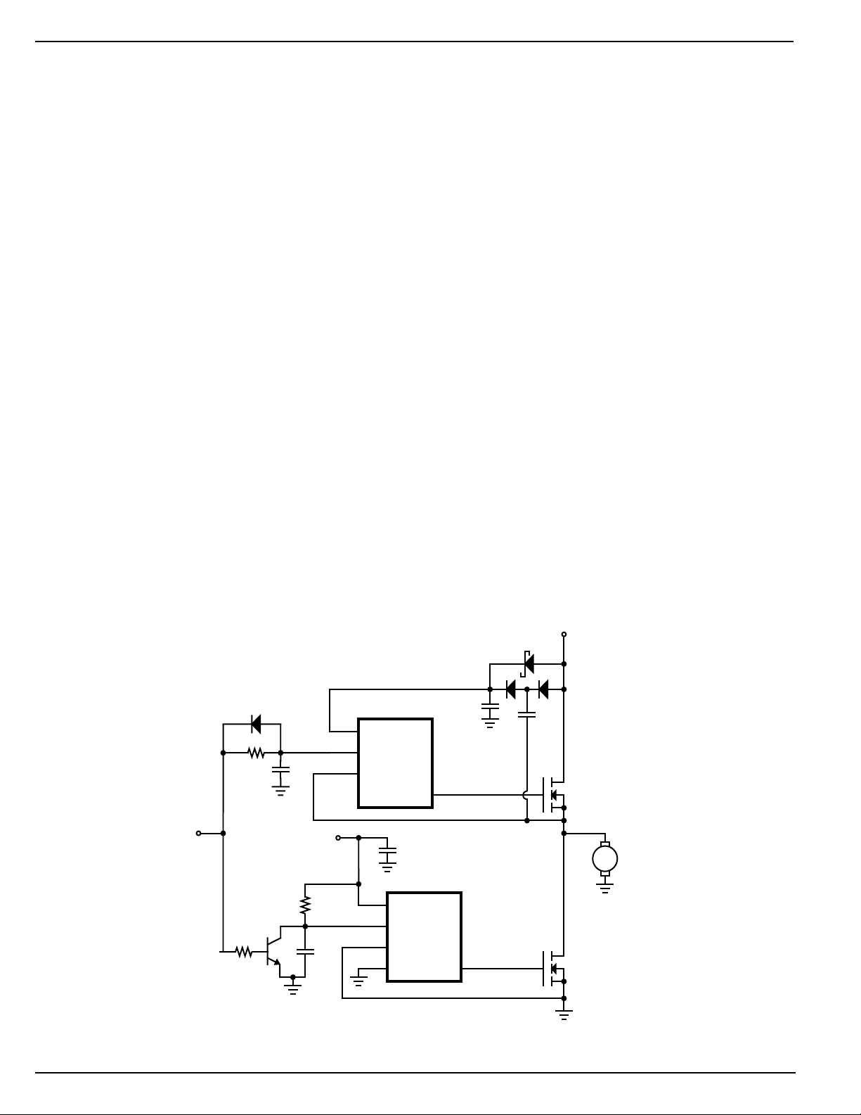
Figure 6. Half-Bridge
Motor Driver
5-120 April 1998
Page 8
MIC5012 Micrel
Applications Information (Continued)
can be paralleled. This reduces the switch drop, and distributes the switch dissipation into multiple packages.
Half-Bridge Motor Driver (Figure 6). Closed loop control of
motor speed requires a half-bridge driver. This topology
presents an extra challenge since the two output devices
should not cross conduct (shoot-through) when switching.
Cross conduction increases output device power dissipation. Speed is also important, since PWM control requires
the outputs to switch in the 2 to 20kHz range.
The circuit of Figure 6 utilizes fast configurations for both the
top- and bottom-side drivers. Delay networks at each input
provide a 2 to 3µs dead time effectively eliminating cross
conduction. Two of these circuits can be connected together to form an H-bridge for locked antiphase or sign/
magnitude control.
Time-Delay Relay (Figure 7). The MIC5012 forms the
basis of a simple time-delay relay. As shown, the delay
commences when power is applied, but the 100kΩ/1N4148
could be independently driven from an external source such
as a switch or another high-side driver to give a delay
relative to some other event in the system. Hysteresis has
been added to guarantee clean switching at turn-on.
Motor Driver with Stall Shutdown (Figure 8). Tachometer
feedback can be used to shut down a motor driver circuit
when a stall condition occurs. The control switch is a 3-way
type; the “START” position is momentary and forces the
driver ON. When released, the switch returns to the “RUN”
position, and the tachometer's output is used to hold the
MIC5012 input ON. If the motor slows down, the tach output
is reduced, and the MIC5012 switches OFF. Resistor “R”
sets the shutdown threshold.
12V
12V
+
IRFZ44
OUTPUT
(Delay=2s)
100kΩ 1N4148
+
47µF
10kΩ
100Ω
1/2 MIC5012
V+
Input
Source
Gnd
Gate
10µF
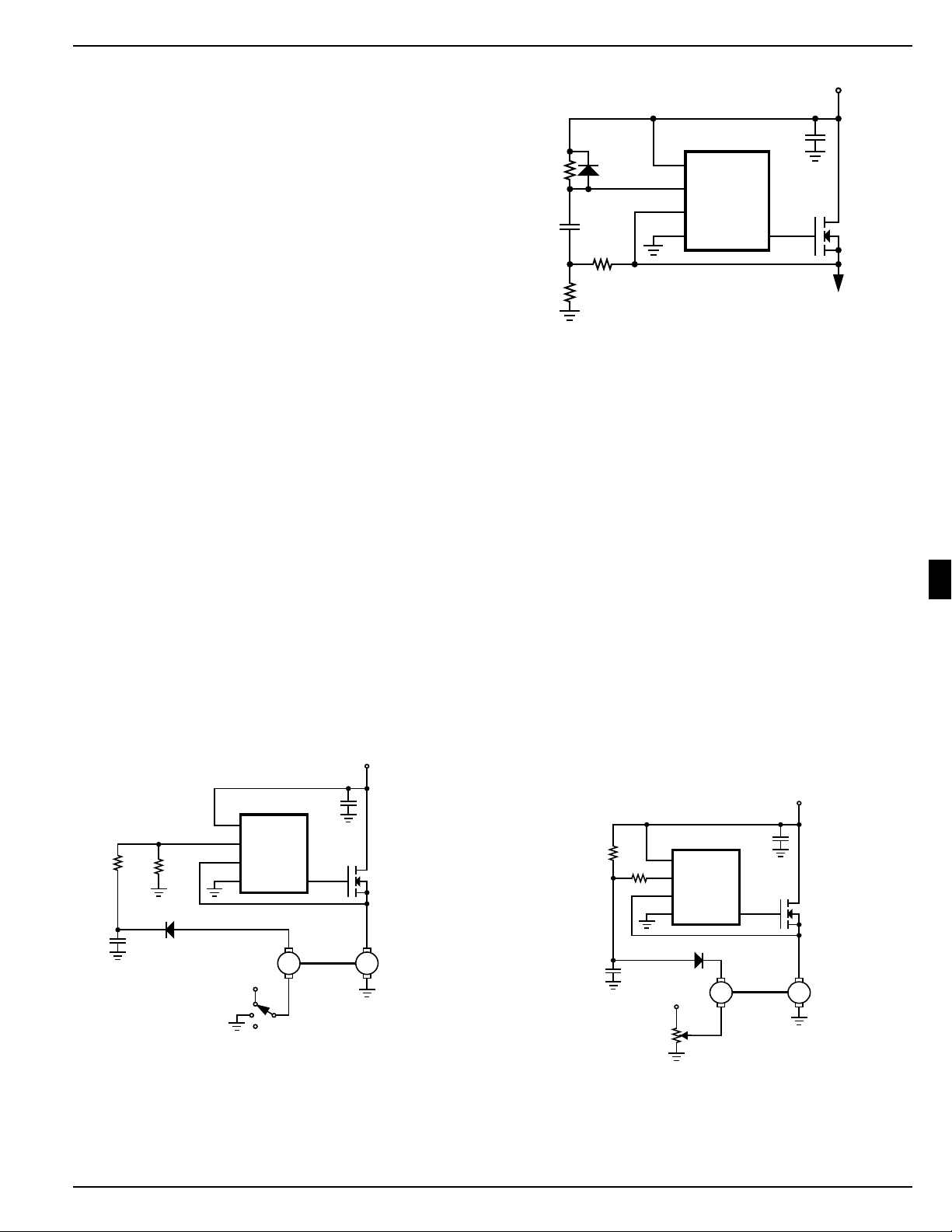
Figure 7. 30 Ampere
Time-Delay Relay
Electronic Governor (Figure 9). The output of an ac
tachometer can be used to form a PWM loop to maintain the
speed of a motor. The tachometer output is rectified,
partially filtered, and fed back to the input of the MIC5012.
When the motor is stalled there is no tachometer output,
and MIC5012 input is pulled high delivering full power to the
motor. If the motor spins fast enough, the tachometer output
is sufficient to pull the MIC5012 input low, shutting the
output off. Since the rectified waveform is only partially
filtered, the input oscillates around its threshold causing the
MIC5012 to switch on and off at the frequency of the
tachometer signal. A PWM action results since the average
dc voltage at the input decreases as the motor spins faster.
The 1kΩ potentiometer is used to set the running speed of
the motor. Loop gain (and speed regulation) is increased by
increasing the value of the 100nF filter capacitor.
The performance of such a loop is imprecise, but stable and
inexpensive. A more elaborate loop would consist of a PWM
controller and a half-bridge.
5
+
Gate
T
10µF
IRFZ44
M
R
100nF
330kΩ330kΩ
1N4148
START
RUN
STOP
Figure 8. Motor Stall
1/2 MIC5012
V+
Input
Source
Gnd
12V
Shutdown
April 1998 5-121
330kΩ
330kΩ
100nF
Figure 9. Electronic Governor
1/2 MIC5012
V+
Input
Source
Gnd
1N4148
15V
1kΩ
Gate
T
10µF
15V
+
IRF541
M
Page 9
MIC5012 Micrel
Applications Information (Continued)
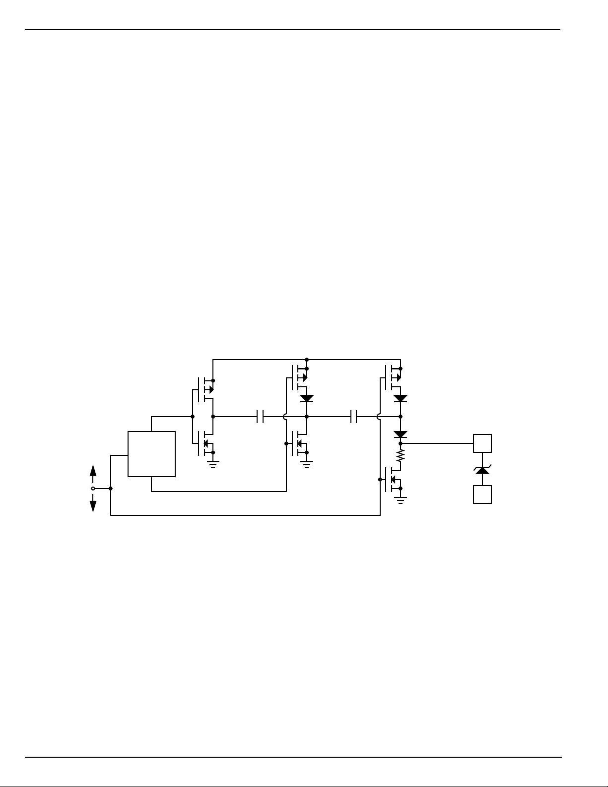
Gate Control Circuit
When applying the MIC5012, it is helpful to understand the
operation of the gate control circuitry (see Figure 12). The
gate circuitry can be divided into two sections: 1) charge
pump (oscillator, Q1-Q5, and the capacitors) and 2) gate
turn-off switch (Q6).
When the MIC5012 is in the OFF state, the oscillator is
turned off, thereby disabling the charge pump. Q5 is also
turned off, and Q6 is turned on. Q6 holds the gate pin (G) at
ground potential which effectively turns the external MOSFET off.
Q6 is turned off when the MIC5012 is commanded on, and
Q5 pulls the gate up to supply (through 2 diodes). Next, the
charge pump begins supplying current to the gate. The gate
accepts charge until the gate-source voltage reaches 12.5V
and is clamped by the zener diode.
A 2-output, three-phase clock switches Q1-Q4, providing a
quasi-tripling action. During the initial phase Q4 and Q2 are
ON. C1 is discharged, and C2 is charged to supply through
Q5. For the second phase Q4 turns off and Q3 turns on,
pushing C2 above supply (charge is dumped into the gate).
Q3 also charges C1. On the third phase Q2 turns off and Q1
turns on, pushing the common point of the two capacitors
above supply. Some of the charge in C1 makes its way to
the gate. The sequence is repeated by turning Q2 and Q4
back on, and Q1 and Q3 off.
In a low-side application operating on a 12 to 15V supply,
the MOSFET is fully enhanced by the action of Q5 alone. On
supplies of more than approximately 14V, current flows
directly from Q5 through the zener diode to ground. To
prevent excessive current flow, the MIC5012 supply should
be limited to 15V in low-side applications.
The action of Q5 makes the MIC5012 operate quickly in
low-side applications. In high-side applications Q5
precharges the MOSFET gate to supply, leaving the charge
pump to carry the gate up to full enhancement 10V above
supply. Bootstrapped high-side drivers are as fast as lowside drivers since the chip supply is boosted well above the
drain at turn-on.
OFF
ON
100 kHz
OSCILLATOR
Q1
Q2
+
V
Q3
125pF125pF
C1 C2
Q4
Figure 10. Gate Control
Circuit Detail
Q5
500Ω
Q6
GATE CLAMP
ZENER
G
12.5V
S
5-122 April 1998
 Loading...