

Page 1
MIC5020 Micrel
MIC5020
Current-Sensing Low-Side MOSFET Driver
General Description
The MIC5020 low-side MOSFET driver is designed to operate at frequencies greater than 100kHz (5kHz PWM for 2% to
100% duty cycle) and is an ideal choice for high-speed
applications such as motor control, SMPS (switch mode
power supplies), and applications using IGBTs. The MIC5020
can also operate as a circuit breaker with or without automatic
retry. The MIC5020’s maximum supply voltage lends itself to
control applications using up to 50V. The MIC5020 can
control MOSFETs that switch voltages greater than 50V.
A rising or falling edge on the input results in a current source
or sink pulse on the gate output. This output current pulse can
turn on or off a 2000pF MOSFET in approximately 175ns.
The MIC5020 then supplies a limited current (< 2mA), if
necessary, to maintain the output state.
An overcurrent comparator with a trip voltage of 50mV makes
the MIC5020 ideal for use with a current sensing MOSFET.
An external low value resistor may be used instead of a
sensing MOSFET for more precise overcurrent control. An
optional external capacitor connected to the CT pin may be
used to control the current shutdown duty cycle from 20% to
< 1%. A duty cycle from 20% to about 75% is possible with
an optional pull-up resistor from CT to VDD. An open collector
output provides a fault indication when the sense inputs are
tripped.
The MIC5020 is available in 8-pin SOIC and plastic DIP
packages.
Other members of the MIC502x series include the MIC5021
high-side driver and the MIC5022 half-bridge driver with a
cross-conduction interlock.
Features
• 11V to 50V operation
• 175ns rise/fall time driving 2000pF
• TTL compatible input with internal pull-down resistor
• Overcurrent limit
• Fault output indication
• Gate to source protection
• Compatible with current sensing MOSFETs
Applications
• Lamp control
• Heater control
• Motor control
• Solenoid switching
• Switch-mode power supplies
• Circuit breaker
Ordering Information
Part Number Temperature Range Package
MIC5020BM –40°C to +85°C 8-pin SOIC
MIC5020BN –40°C to +85°C 8-pin Plastic DIP
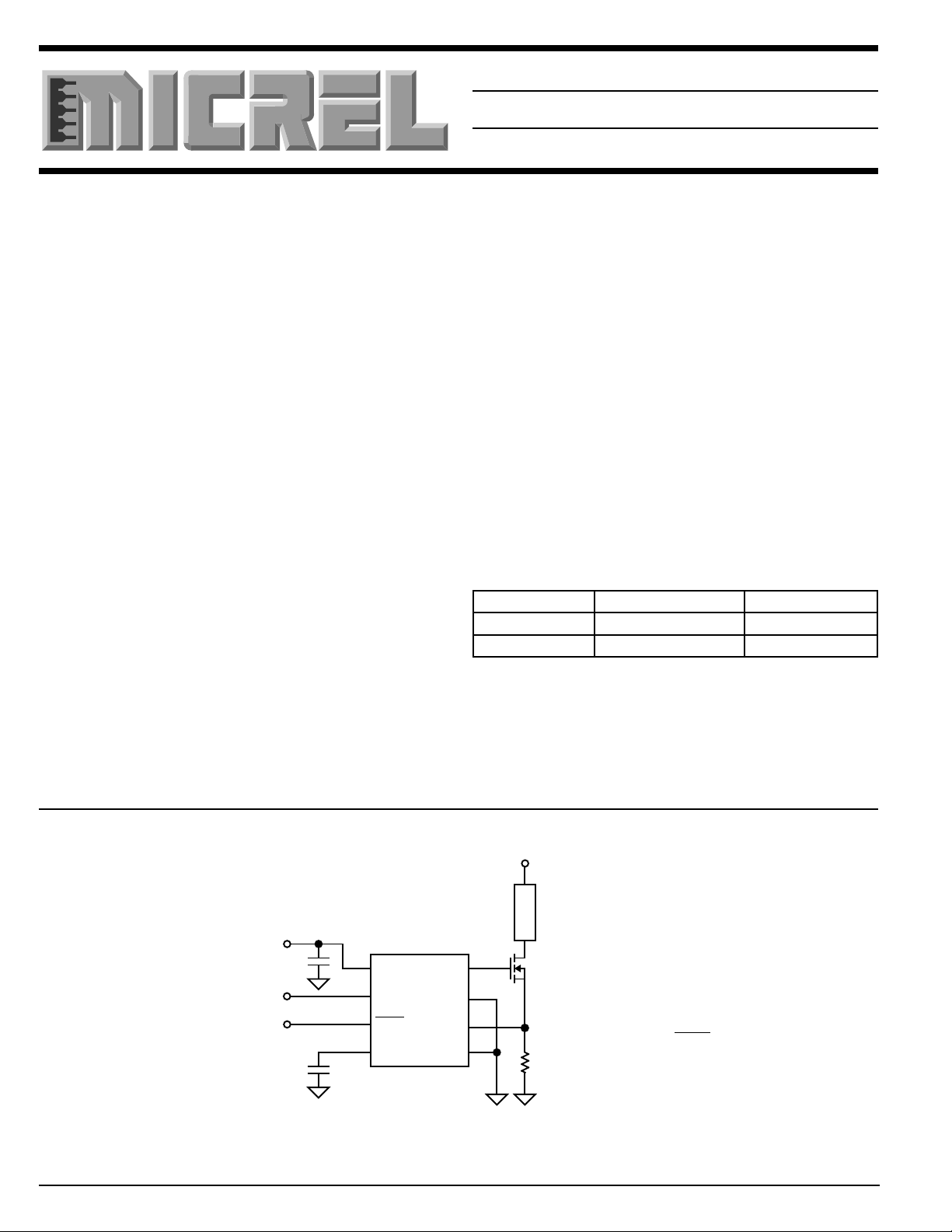
Typical Application
+11V to +50V
150kHz max.
V+
Load
MIC5020
10µF
optional*
1
2
3
4
V
DD
Input
Fault
C
T
Sense−
Sense+
Gate
Gnd
8
7
6
5
N-Channel
Power MOSFET
R
SENSE
* increases time before retry
Low-Side Driver with Overcurrent Trip and Retry
5-162 October 1998
R
SENSE
=
50mV
I
TRIP
Page 2
MIC5020 Micrel
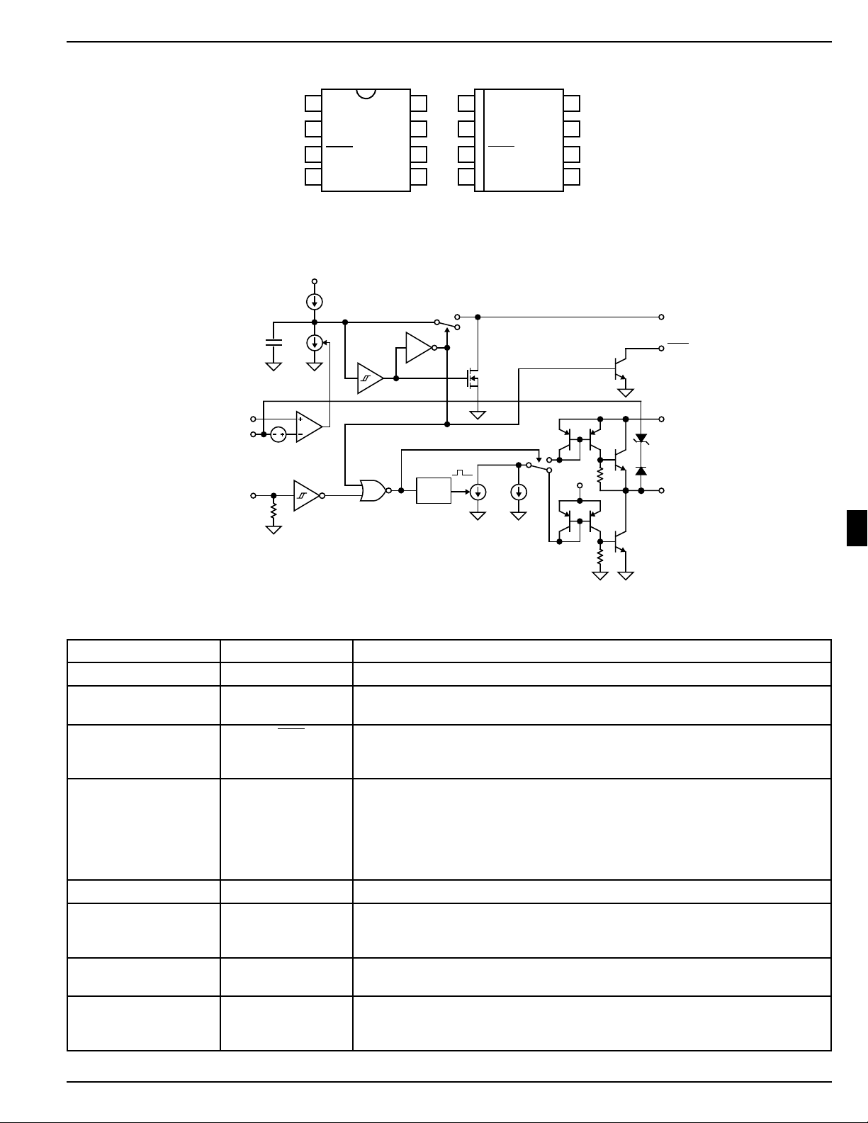
Pin Configuration
Block Diagram
Sense +
Sense –
Input
1
V
DD
Input
2
Fault
3
C
4
T
DIP Package SOIC Package
6V Internal Regulator
I
1
C
INT
2I
1
50mV
8
Gate
Sense−
Sense+
Gnd
7
6
5
1
V
DD
Input
2
3
4
Fault
C
T
Sense−
Sense+
(N) (M)
Fault
Normal
Q1
↑
↓
ONE-
SHOT
10I
2
Gate
Gnd
I
2
8
7
6
5
C
T
Fault
V
DD
ON
OFF
6V
Gate
Transistor Count: 82
Pin Description
Pin Number Pin Name Pin Function
1V
2 Input TTL Compatible Input: Logic high turns the external MOSFET on. An internal
3 Fault Overcurrent Fault Indicator: When the sense voltage exceeds threshold,
4C
5 Gnd Circuit Ground
6 Sense + Current Sense Comparator (+) Input: Connect to high side of sense resistor
7 Sense – Current Sense Comparator (–) Input: Connect to the low side of the sense
8 Gate Gate Drive: Drives the gate of an external power MOSFET. Also limits V
DD
T
Supply: +11V to +50V. Decouple with ≥ 10µF capacitor.
pull-down returns an open pin to logic low.
open collector output is open circuit for 5µs (t
t
G(OFF)
. t
is adjustable from CT.
G(OFF)
Retry Timing Capacitor: Controls the off time (t
retry cycle. (Duty cycle adjustment.)
), then pulled low for
G(ON)
) of the overcurrent
G(OFF)
• Open = 20% duty cycle.
• Capacitor to Ground = approx. 20% to <1% duty cycle.
• Pull-Up resistor = approx. 20% to approx. 75% duty cycle.
• Ground = maintained shutdown upon overcurrent condition.
or current sensing MOSFET sense lead. A built-in offset in conjunction with
R
sets the load overcurrent trip point.
SENSE
resistor (usually power ground).
to 15V max. to prevent Gate to Source damage. Will sink and source
GS
current.
5
October 1998 5-163
Page 3

MIC5020 Micrel
Absolute Maximum Ratings
Supply Voltage (VDD) ..................................................+55V
Input Voltage ................................................ –0.5V to +15V
Sense Differential Voltage..........................................±6.5V
Sense + or Sense – to Gnd.......................... –0.5V to +50V
Operating Ratings
Supply Voltage (VDD) ....................................+11V to +50V
Temperature Range
SOIC ...................................................... –40°C to +85°C
Plastic DIP..............................................–40°C to +85°C
Fault Voltage ...............................................................+50V
Current into Fault .......................................................50mA
Timer Voltage (CT) .....................................................+5.5V
Electrical Characteristics
TA = 25°C, Gnd = 0V, VDD = 12V, Sense +,– = 0V, Fault = Open, CT = Open, Gate CL = 1500pF unless otherwise specificed
Symbol Parameter Condition Min Typ Max Units
D.C. Supply Current VDD = 12V, Input = 0V 0.8 2 mA
VDD = 50V, Input = 0V 2 10 mA
VDD = 12V, Input = 5V 0.8 2 mA
VDD = 50V, Input = 5V 4 25 mA
Input Threshold 0.8 1.4 2.0 V
Input Hysteresis 0.1 V
Input Pull-Down Current Input = 5V 10 20 40 µA
Fault Output Fault Current = 1.6mA 0.15 0.4 V
Saturation Voltage Note 1
Fault Output Leakage Fault = 50V –1 0.01 +1 µA
Current Limit Threshold Note 2 30 50 70 mV
Gate On Voltage VDD = 12V 10 11 V
VDD = 50V 14 15 18 V
t
G(ON)
t
G(OFF)
t
DLH
t
R
t
DLH
t
F
f
max
Note 1 Voltage remains low for time affected by CT.
Note 2 When using sense MOSFETs, it is recommended that R
Note 3 Input switched from 0.8V (TTL low) to 2.0V (TTL high), time for Gate transition from 0V to 2V.
Note 4 Input switched from 0.8V (TTL low) to 2.0V (TTL high), time for Gate transition from 2V to 10V.
Note 5 Input switched from 2.0V (TTL high) to 0.8V (TTL low), time for Gate transition from 11V (Gate ON voltage) to 10V.
Note 6 Input switched from 2.0V (TTL high) to 0.8V (TTL low), time for Gate transition from 10V from 2V.
Note 7 Frequency where gate on voltage reduces to 10V with 50% input duty cycle.
Gate On Time, Fixed Sense Differential > 70mV 2 5 10 µs
Gate Off Time, Adjustable Sense Differential > 70mV, CT = 0pF 10 20 50 µs
Gate Turn-On Delay Note 3 400 800 ns
Gate Rise Time Note 4 700 1500 ns
Gate Turn-Off Delay Note 5 900 1500 ns
Gate Fall Time Note 6 500 1500 ns
Maximum Operating Frequency Note 7 100 150 kHz
< 50Ω. Higher values may affect the sense MOSFET’s current transfer ratio.
SENSE
5-164 October 1998
Page 4
MIC5020 Micrel
200
400
600
800
1000
1200
1x10
2
1x10
3
1x10
4
1x10
5
t
ON
(ns)
C
GATE
(pF)
0.0
5.0
10.0
15.0
20.0
25.0
0.1 1 10 100 1000 10000
Shutdown Duty Cycle (%)
CT (pF)
400
500
600
700
800
900
5 101520253035404550
t
ON
(nS)
V
SUPPLY
(V)
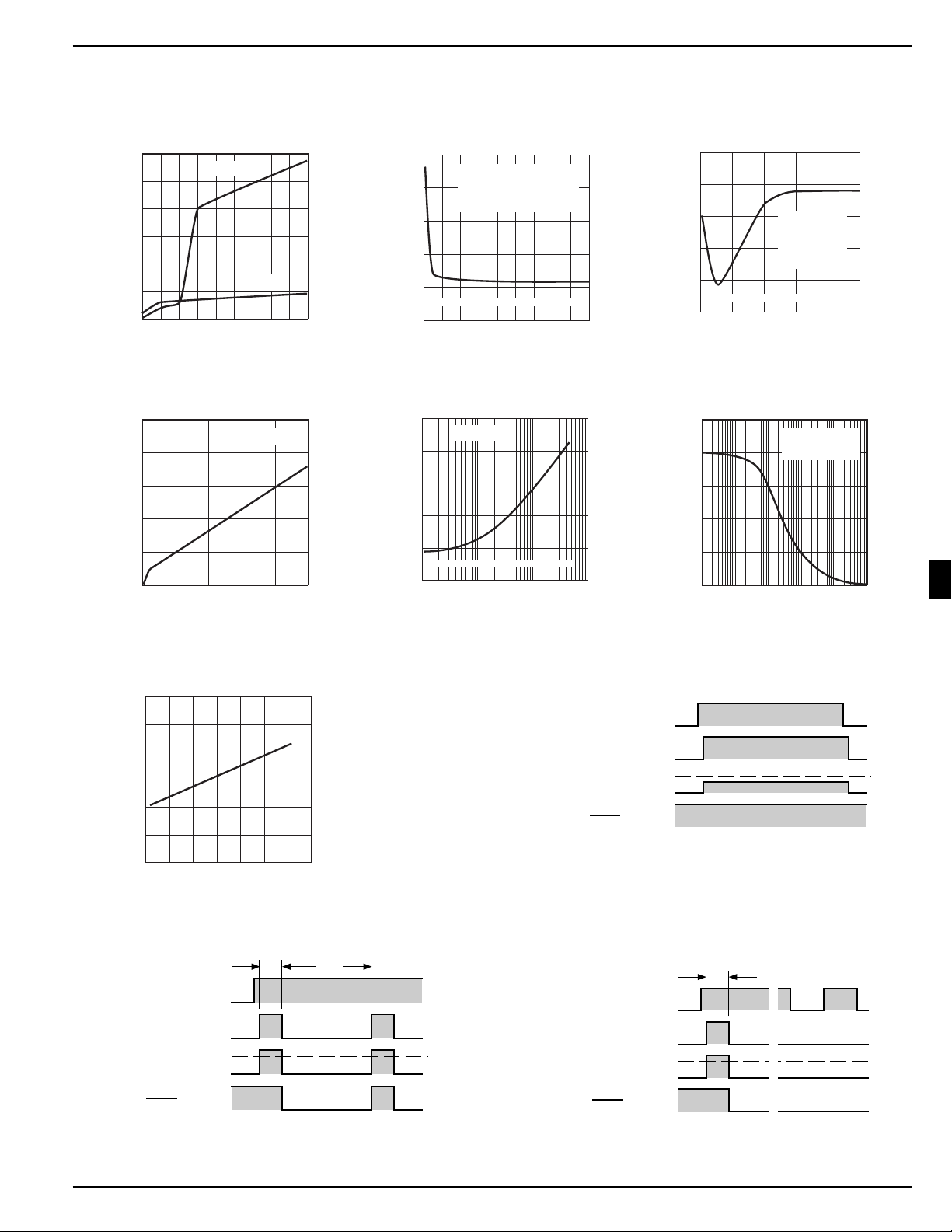
Typical Characteristics
Supply Current vs.
3.5
3.0
2.5
(mA)
2.0
SUPPLY
1.5
I
1.0
0.5
Supply Voltage
VIN = 5V
VIN = 0V
5 101520253035404550
V
SUPPLY
(V)
Input Current vs.
100
(µA)
I
80
60
IN
40
20
0
Input Voltage
V
SUPPLY
0 5 10 15 20 25
VIN (V)
= 12V
Turn-On Time vs.
Supply Voltage
V
= 4V
GATE
= 1500pF
C
L
= 0 to 5V Sq. Wave
V
IN
INCLUDES PROPAGATION DELAY
Turn-On Time vs.
Gate Capacitance
V
= 4V
GATE
INCLUDES PROPAGATION DELAY
Turn-Off Time vs.
1200
1100
1000
(ns)
OFF
t
900
800
700
Supply Voltage
V
= 4V
GATE
= 1500pF
C
L
= 0 to 5V
V
IN
Sq. Wave
INCLUDES PROPAGATION DELAY
5 1015202530
V
SUPPLY
(V)
Overcurrent Shutdown
Retry Duty Cycle
tON = 5µs
V
SUPPLY
= 12V
5
Sense Threshold vs.
80
70
60
50
40
VOLTAGE (mV)
30
20
-60 -30 0 30 60 90 120 150
Input
Gate
Sense +, –
Differential
Fault
Timing Diagram 2. Fault Condition, CT = Open Timing Diagram 3. Fault Condition, CT = Grounded
October 1998 5-165
Temperature
TEMPERATURE (°C)
5µs
TTL (H)
0V
15V (max.)
0V
50mV
0V
Off
On
20µs
Input
Gate
Sense +, –
Differential
Fault
TTL (H)
0V
15V (max.)
0V
50mV
0V
Off
On
Timing Diagram 1. Normal Operation
5µs
0V
0V
0V
Off
On
Input
Gate
Sense +, –
Differential
Fault
TTL (H)
15V (max.)
50mV
Page 5

MIC5020 Micrel
Functional Description
Refer to the MIC5020 block diagram.
Input
A signal greater than 1.4V (nominal) applied to the MIC5020
INPUT causes gate enhancement on an external MOSFET
turning the external MOSFET on.
An internal pull-down resistor insures that an open INPUT
remains low, keeping the external MOSFET turned off.
Gate Output
Rapid rise and fall times on the GATE output are possible
because each input state change triggers a one-shot which
activates a high-value current sink (10I2) for a short time. This
draws a high current through a current mirror circuit causing
the output transistors to quickly charge or discharge the
external MOSFET’s gate.
A second current sink continuously draws the lower value of
current used to maintain the gate voltage for the selected
state.
An internal 15V Zener diode protects the external MOSFET
by limiting the gate output voltage when VDD is connected to
higher voltages.
Overcurrent Limiting
Current source I1 charges C
upon power up. An optional
INT
external capacitor connected to CT is discharged through
MOSFET Q1.
A fault condition (> 50mV from SENSE + to SENSE –) causes
the overcurrent comparator to enable current sink 2I1 which
overcomes current source I1 to discharge C
When C
is discharged, the INPUT is disabled, which turns
INT
off the GATE output; the FAULT output is enabled; and C
in a short time.
INT
INT
and CT are ready to be charged.
When the GATE output turns the MOSFET off, the overcurrent
signal is removed from the sense inputs which deactivates
current sink 2I1. This allows C
and the optional capacitor
INT
connected to CT to recharge. A Schmitt trigger delays the
retry while the capacitor(s) recharge. Retry delay is increased by connecting a capacitor to CT (optional).
The retry cycle will continue until the the fault is removed or
the input is changed to TTL low.
If CT is connected to ground, the circuit will not retry upon a
fault condition.
Fault Output
The FAULT output is an open collector transistor. FAULT is
active at approximately the same time the output is disabled
by a fault condition (5µs after an overcurrent condition is
sensed). The FAULT output is open circuit (off) during each
successive retry (5µs).
Applications Information
The MIC5020 MOSFET driver is intended for low-side switching applications where higher supply voltage, overcurrent
sensing, and moderate speed are required.
Supply Voltage
A feature of the MIC5020 is that its supply voltage rating of up
to 50V is higher than many other low-side drivers.
The minimum supply voltage required to fully enhance an Nchannel MOSFET is 11V.
A lower supply voltage may be used with logic level MOSFETs.
Approximately 6V is needed to provide 5V of gate enhancement.
Low-Side Switch Circuit Advantages
A moderate-speed low-side driver is generally much faster
than a comparable high-side driver. The MIC5020 can
provide the gate drive switching times and low propagation
delay times that are necessary for high-frequency highefficiency circuit operation in PWM (pulse width modulation)
designs used for motor control, SMPS (switch mode power
supply) and heating element control. Switched loads (on/off)
can benefit from the MIC5020’s fast switching times by
allowing use of MOSFETs with smaller safe operating areas.
(Larger MOSFETs are often required when using slower
drivers.)
Overcurrent Limiting
A 50mV comparator is provided for current sensing. The low
level trip point minimizes I2R losses when power resistors are
used for current sensing. Flexibility in choosing drain or
source side sensing is provided by access to both SENSE +
and SENSE – comparator inputs.
The adjustable retry feature can be used to handle loads with
high initial currents, such as lamps, motors, or heating
elements and can be adjusted from the CT connection.
CT to ground causes maintained gate drive shutdown following overcurrent detection.
CT open, or through a capacitor to ground, causes automatic
retry . The default duty cycle (CT open) is approximately 20%.
Refer to the electrical characteristics when selecting a capacitor for a reduced duty cycle.
CT through a pull-up resistor to VDD increases the duty cycle.
Increasing the duty cycle increases the power dissipation in
the load and MOSFET.
Circuits may become unstable at a
duty cycles of about 75% or higher, depending on the
conditions.
Caution: The MIC5020 may be damaged if the
voltage on CT exceeds the absolute maximum rating.
An overcurrent condition is externally signaled by an open
collector (FAULT) output.
The MIC5020 may be used without current sensing by
connecting SENSE + and SENSE – to ground.
Current Sense Resistors
Lead length can be significant when using low value (< 1Ω)
resistors for current sensing. Errors caused by lead length
can be avoided by using four-terminal current sensing resistors. Four-terminal resistors are available from several
manufacturers.
5-166 October 1998
Page 6
MIC5020 Micrel
V
DD
Input
Fault
C
T
Gate
Sense−
Sense+
Gnd
TTL Input
(0V/5V)
N-Channel
Current Sensing
Power MOSFET
V+
MIC5020
1
2
3
4
8
7
6
5
10µF
Load
R
SENSE
(10Ω)
+11V to +50V
(+13.2V)
(+13.2V, > 4.4A)
(IRCZ24)
(3Ω, > 60W)
“( )” values apply to
demo circuit. See text.
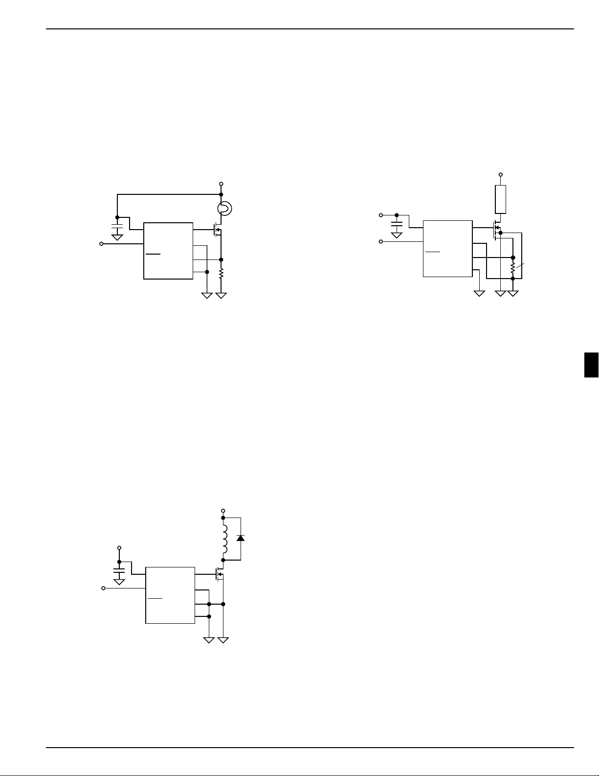
Lamp Driver Application
Incandescent lamps have a high inrush current (low resistance) when turned on. The MIC5020 can perform a “soft
start” by pulsing the MOSFET (overcurrent condition) until
the filament is warm enough for its current to decrease
(resistance increases). The sense resistor is selected so the
voltage across the sense resistor drops below the sense
threshold (50mV) as the filament becomes warm. The
MOSFET is no longer pulsed to limit current and the lamp
turns completely on.
V+
(+11V to +12V)
Incandescent
Lamp (#1157)
N-Channel
Power MOSFET
(IRF540)
R
SENSE
(0.041Ω)
10µF
TTL Input
(0V/5V)
demo circuit. See text.
1
V
DD
2
Input
3
Fault
4
C
T
“( )” values apply to
MIC5020
Sense−
Sense+
Gate
Gnd
8
7
6
5
Figure 1. Lamp Driver with
Current Sensing
A lamp may not fully turn on if the filament does not heat up
adequately. Changing the duty cycle, sense resistor, or both
to match the filament characteristics can correct the problem.
Soft start can be demonstrated using a #1157 dual-filament
automotive lamp. The value of RS shown in figure 1 allows for
soft start of the higher-resistance filament (measures approx.
2.1Ω cold or 21Ω hot).
Solenoid Driver Application
The MIC5020 can be directly powered by the control voltage
supply in typical 11Vdc through 50Vdc control applications.
Current sensing has been omitted as an example.
V+
+11V to +50V
MIC5020
10µF
TTL Input
1
V
DD
2
Input
3
Fault
4
C
T
Figure 2. Solenoid Driver,
Without Current Sensing
A diode across the load protects the MOSFET from the
voltage spike generated by the inductive load upon MOSFET
turn off. The peak forward current rating of the diode should
be greater than the load current.
October 1998 5-167
Solenoid
8
Gate
7
Sense−
6
Sense+
5
Gnd
Diode
N-Channel
Power MOSFET
Current Sensing MOSFET Application
A current sensing MOSFET allows current sensing without
adding additional resistance to the power switching circuit.
A current sensing MOSFET has two source connections: a
“power source” for power switching and a “current source” for
current sensing. The current from the current source is
approximately proportional to the current through the power
source, but much smaller. A current sensing ratio (I
I
) is provided by the MOSFET manufacturer.
SENSE
SOURCE
Figure 3. Using a Current Sensing MOSFET
The MOSFET current source is used to develop a voltage
across a sense resistor. This voltage is monitored by the
MIC5020 (SENSE + and SENSE – pins) to identify an overcurrent condition.
The value of the sense resistor can be estimated with:
R
SENSE
= (r V
TRIP
R
DS(ON)
) / (I
LOAD RDS(ON)
– V
TRIP
)
where:
R
V
r = manufacturer’s current sense ratio: (I
R
I
LOAD
= external “sense” resistor
SENSE
= 50mV (0.050V) for the MIC5020
TRIP
= manufacturer’s power source on resistance
DS(ON)
= load current (power source current)
SOURCE/ISENSE
The drain to source voltage under different fault conditions
affects the behavior of the MOSFET current source; that is,
the current source will respond differently to a slight overcurrent condition (V
(where V
is approximately equal to the supply voltage).
DS(ON)
very small) than to a short circuit
DS(ON)
Adjustment of the sense resistor value by experiment starting
from the above formula will provide the quickest selection of
R
SENSE
.
Refer to manufacture’s data sheets and application notes for
detailed information on current sensing MOSFET characteristics.
Figure 3 includes values which can be used to demonstrate
circuit operation. The IRCZ24 MOSFET has a typical sense
ratio of 780 and a R
of 0.10Ω. A large 3Ω wirewound
DS(ON)
load resistor will cause inductive spikes which should be
suppressed using a diode (using the same configuration as
figure 2).
/
5
)
Page 7
MIC5020 Micrel
+
+
Faster MOSFET Switching
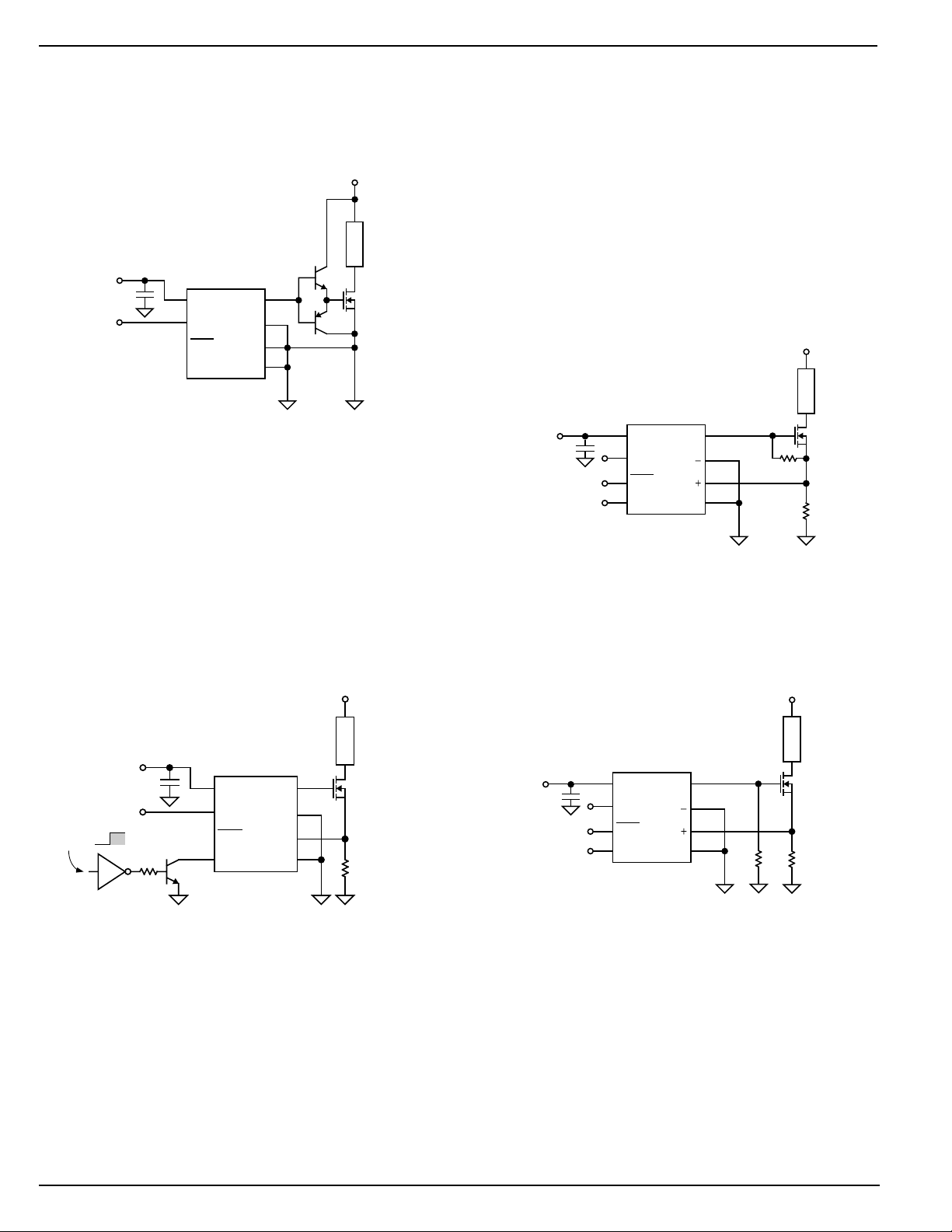
The MIC5020’s GATE current can be multiplied using a pair
of bipolar transistors to permit faster charging and discharging of the external MOSFET’s gate.
+40V max.
Load
Gate
Gnd
2N3904
8
7
6
5
2N3906
N-Channel
Power MOSFET
(IRF540)
+11V to +50V
150kHz max.
10µF
1
2
3
4
MIC5020
V
DD
Input
Fault
C
T
Sense−
Sense+
Figure 4. Faster MOSFET Switching Circuit
NPN and PNP transistors are used to respectively charge
and discharge the MOSFET gate. The MIC5020 gate current
is multiplied by the transistor β.
The switched circuit voltage can be increased above 40V by
selecting transistors with higher ratings.
Remote Overcurrent Limiting Reset
In circuit breaker applications where the MIC5020 maintains
an off condition after an overcurrent condition is sensed, the
CT pin can be used to reset the MIC5020.
For test purposes, a 680Ω load resistor and 3Ω sense resistor
will produce an overcurrent condition when the load’s supply
(V+) is approximately 12V or greater.
Low-Temperature Operation
As the temperature of the MIC5020AJB (extended temperature range version—no longer available) approaches –55°C,
the driver’s off-state, gate-output offset from ground increases. If the operating environment of the MIC5020AJB
includes low temperatures (–40°C to –55°C), add an external
2.2MΩ resistor as shown in Figures 6a or 6b. This assures
that the driver’s gate-to-source voltage is far below the
external MOSFET’s gate threshold voltage, forcing the
MOSFET fully off.
V+
Load
11V to +50V
10µF
1
2
3
4
MIC5020
V
DD
Input
Fault
C
T
Gate
Sense
Sense
Gnd
8
7
R
2.2M
SENSE
6
5
Figure 6a. Gate-to-Source Pull Down
The gate-to-source configuration (refer to Figure 6a) is appropriate for resistive and inductive loads. This also causes
the smallest decrease in gate output voltage.
V+
Load
+11V to +50V
Retry (H)
Maintained (L)
TTL input
74HC04
(example)
10µF
10k to
100k
Q1
2N3904
1
2
3
4
MIC5020
V
DD
Input
Fault
C
T
Gate
Sense−
Sense+
Gnd
8
7
6
5
N-Channel
Power MOSFET
R
Figure 5. Remote Control Circuit
Switching Q1 on pulls CT low which keeps the MIC5020 GATE
output off when an overcurrent is sensed. Switching Q1 off
causes CT to appear open. The MIC5020 retries in about
20µs and continues to retry until the overcurrent condition is
removed.
SENSE
V+
Load
11V to +50V
10µF
1
2
3
4
MIC5020
V
DD
Input
Fault
C
T
Gate
Sense
Sense
Gnd
8
7
6
5
2.2M
R
SENSE
Figure 6b. Gate-to-Ground Pull Down
The gate-to-ground configuration (refer to Figure 6b) is
appropriate for resistive, inductive, or capacitive loads. This
configuration will decrease the gate output voltage slightly
more than the circuit shown in Figure 6a.
5-168 October 1998
 Loading...