

Page 1
MIC5022 Micrel
MIC5022
Half-Bridge MOSFET Driver
General Description
The MIC5022 half-bridge MOSFET driver is designed to
operate at frequencies up to 100kHz (5kHz PWM for 2% to
100% duty cycle) and is an ideal choice for high speed
applications such as motor control and SMPS (switch mode
power supplies).
A rising or falling edge on the input results in a current source
pulse or sink pulse on the gate outputs. This output current
pulse can turn on a 2000pF MOSFET in approximately 1µs.
The MIC5022 then supplies a limited current (< 2mA), if
necessary, to maintain the output states.
Two overcurrent comparators with nominal trip voltages of
50mV make the MIC5022 ideal for use with current sensing
MOSFETs. External low value resistors may be used instead
of sensing MOSFETs for more precise overcurrent control.
Optional external capacitors placed on the C
may be used to individually control the current shutdown duty
cycles from approximately 20% to <1%. Duty cycles from
20% to about 75% are possible with individual pull-up resistors from CTL and CTH to VDD. An open collector output
provides a fault indication when either sense input is tripped.
The MIC5022 is available in 16-pin wide SOIC and 14-pin
plastic DIP packages.
Other members of the MIC502x family include the MIC5020
low-side driver and the MIC5021 high-side driver.
and CTL pins
TH
Features
• 12V to 36V operation
• 600ns rise time into 1000pF (high side)
• TTL compatible input with internal pull-down resistor
• Outputs interlocked to prevent cross conduction
• TTL compatible enable
• Fault output indication
• Individual overcurrent limits
• Gate protection
• Internal charge pump (high-side)
• Current source drive scheme reduces EMI
Applications
• Motor control
• Switch-mode power supplies
Ordering Information
Part Number Temperature Range Package
MIC5022BWM –40°C to +85°C 16-pin Wide SOIC
MIC5022BN –40°C to +85°C 14-pin Plastic DIP
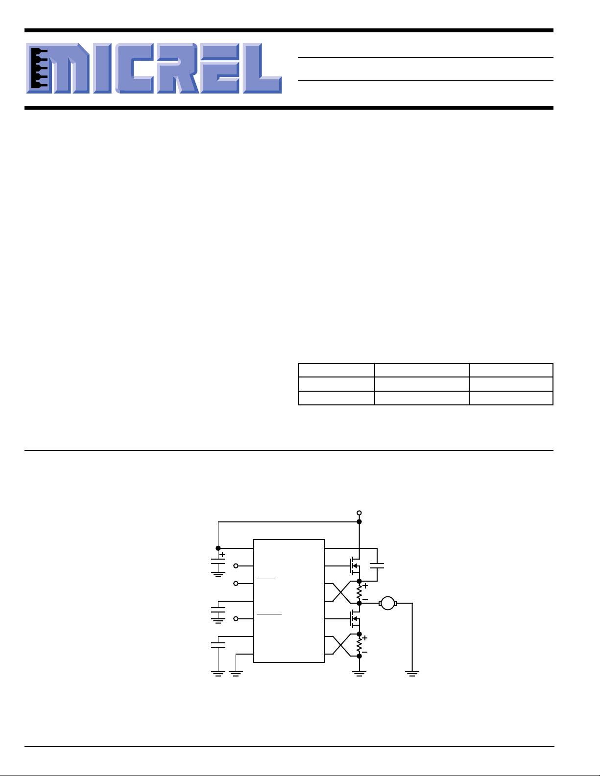
Typical Application
TTL Input
PWM signal)
MIC5022
1
V
2
3
4
5
6
7
DD
Input
Fault
C
TH
Enable
C
TL
Gnd
10µF
C
TH
C
TL
V
BOOST
Gate H
Sense H–
Sense H+
Gate L
Sense L–
Sense L+
DC Motor Control Application
+12V to +36V
14
13
12
11
10
9
8
R
R
2.7nF
S1
M
S2
MIC5022 178 September 1999
Page 2
MIC5022 Micrel
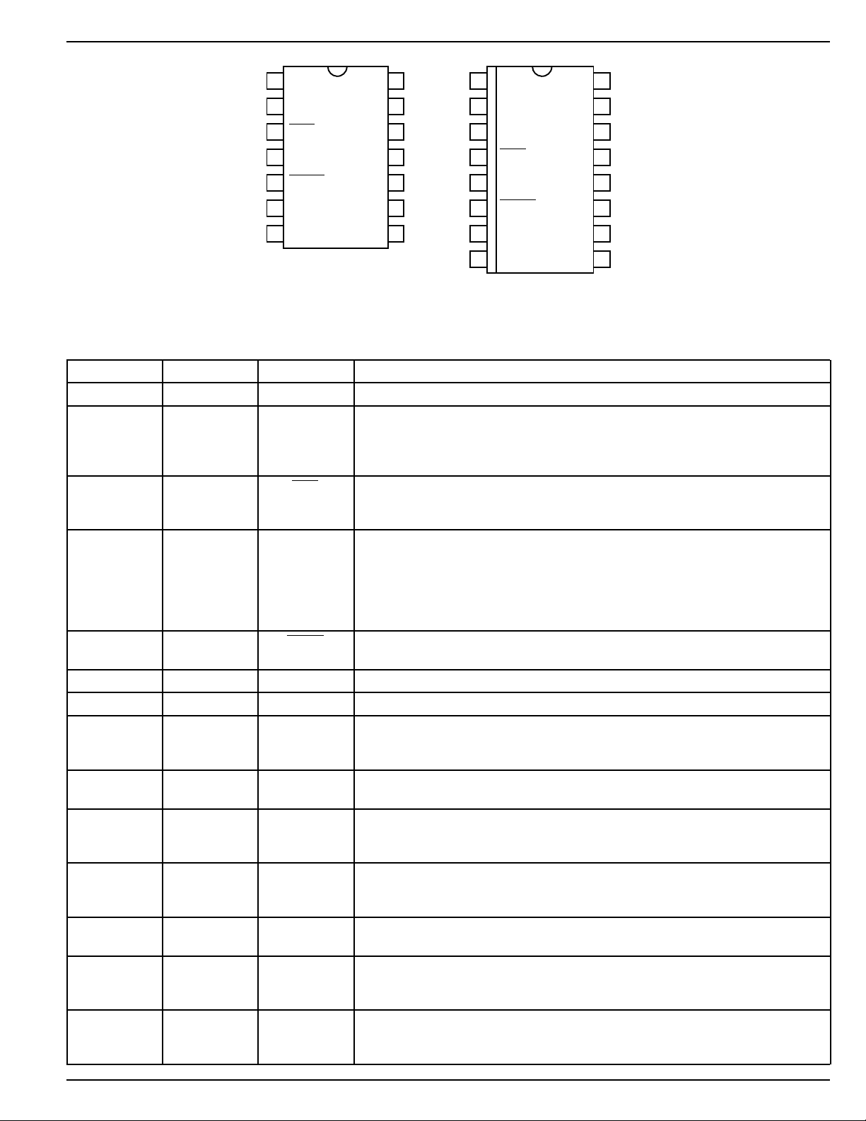
Pin Configuration
114
V
DD
2
Input
3
Fault
V
BOOST
Gate H
Sense H–
13
12
1
V
DD
2
NC
3
Input
NC
V
BOOST
Gate H
16
15
14
4
5
6
7
C
TH
Enable
C
TL
Gnd
Sense H+
Gate L
Sense L–
Sense L+
11
10
4
Fault
Sense H–
5
C
Sense H+
TH
8
6
7
Enable
C
TL
Gnd
Sense L–
Sense L+
9
8
Gate L
13
12
11
10
9
DIP Package SOIC Package
(N) (WM)
Pin Description
DIP Pin No. SOIC Pin No. Pin Name Pin Function
11VDDSupply: +12V to +36V. Decouple with ≥ 10µF capacitor.
2 3 Input TTL Compatible Input: Logic high turns the high-side external MOSFET on
and the low-side external MOSFET off. Logic low turns the high-side
external MOSFET off and the low-side external MOSFET on. An internal
pull-down returns an open pin to logic low.
3 4 Fault When either sense voltage exceeds threshold, open collector output is open
circuit for 5µs (t
CT.
45C
TH
Retry Trimming Capacitor, High Side: Controls the off time (t
overcurrent retry cycle. (Duty cycle adjustment.)
• Open = approx. 20% duty cycle.
• Capacitor to Ground = approx. 20% to < 1% duty cycle.
• Pullup resistor = approx. 20% to approx. 75% duty cycle.
• Ground = maintained shutdown upon overcurrent condition.
5 6 Enable Output Enable: Disables operation of the output drivers; active high. An
internal pull-down returns an open pin to logic low.
67CTLRetry Trimming Capacitor, Low Side: Same function as CTH.
7 8 Gnd Circuit Ground
8 8 Sense L + Current Sense Comparator (+) Input, Low Side: Connect to source of low-
side MOSFET. A built-in offset (nominal 50mV) in conjunction with R
sets the load overcurrent trip point.
9 10 Sense L – Current Sense Comparator (–) Input, Low Side: Connect to the negative
side of the low-side sense resistor.
10 11 Gate L Gate Drive, Low Side: Drives the gate of an external power MOSFET. Also
limits VGS to 15V max. to prevent Gate to Source damage. Will sink and
source current.
11 12 Sense H + Current Sense Comparator (+) Input, High Side: Connect to source of high-
side MOSFET. A built-in offset (nominal 50mV) in conjunction with R
sets the load overcurrent trip point.
12 13 Source H – Current Sense Comparator (–) Input, High Side: Connect to the negative
side of the high-side sense resistor.
13 14 Gate H Gate Drive, High Side: Drives the gate of an external power MOSFET. Also
limits VGS to 15V max. to prevent Gate to Source damage. Will sink and
source current.
14 15 V
BOOST
Charge Pump Boost Capacitor: A bootstrap capacitor from V
MOSFET source pin supplies charge to quickly enhance the external
MOSFET’s gate .
), then pulled low for t
G(ON)
G(OFF)
. t
is adjustable from
G(OFF)
G(OFF)
BOOST
) of the
SENSE
SENSE
to the
September 1999 179 MIC5022
Page 3
MIC5022 Micrel
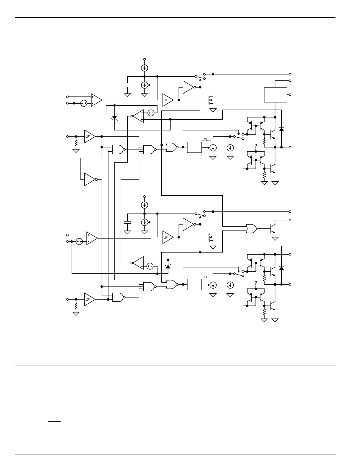
Block Diagram
6V Internal Regulator
I
Sense H+
Sense H–
50mV
15V
1
C
INT
2I
1
1.4V
Fault
Normal
Q1
CHARGE
PUMP
C
V
V
TH
DD
BOOST
Input
Sense L+
Sense L–
Enable
50mV
ON
OFF
↑
ONE-
SHOT
↓
6V
I
1
C
INT
2I
1
1.4V
15V
↑
↓
ONE-
SHOT
Fault
Normal
Q1
10I
10I
I
2
I
2
6V
2
ON
OFF
6V
2
Gate H
C
TL
Fault
V
DD
Gate L
Transistor Count: 188
Absolute Maximum Ratings
Supply Voltage (VDD) ..................................................+40V
Input Voltage .................................................. –0.5V to 15V
Sense Differential Voltage..........................................±6.5V
Sense + or Sense – to Gnd.......................... –0.5V to +36V
Operating Ratings
Supply Voltage (VDD) ....................................+12V to +36V
Temperature Range
SOIC ...................................................... –40°C to +85°C
PDIP....................................................... –40°C to +85°C
Fault Voltage ...............................................................+36V
Current into Fault .......................................................50mA
Timer Voltage (CT) .....................................................+5.5V
V
Capacitor .................................................... 0.01µF
BOOST
MIC5022 180 September 1999
Page 4

MIC5022 Micrel
Electrical Characteristics
TA = 25°C, Gnd = 0V, VDD = 12V, Gate CL = 1500pF (IRF540 MOSFET) unless otherwise specificed
Symbol Parameter Condition Min Typ Max Units
D.C. Supply Current VDD = 12V, Input = 0V 2.5 5 mA
VDD = 36V, Input = 0V 6.0 10 mA
VDD = 12V, Input = 5V 2.4 5 mA
VDD = 36V, Input = 5V 3.0 25 mA
Input Threshold 0.8 1.4 2.0 V
Input Hysteresis 0.1 V
Input Pull-Down Current Input = 5V 10 20 40 µA
Enable Threshold 0.8 1.4 2.0 V
Enable Hysteresis 0.1 V
Fault Output Fault Current = 1.6mA 0.15 0.4 V
Saturation Voltage Note 1
Fault Output Leakage Fault = 36V –1 0.01 +1 µA
Current Limit Thresh., Low-Side Note 2 30 50 70 mV
Current Limit Thresh., High-Side Note 2 30 50 70 mV
Gate On Voltage, High-Side VDD = 12V, Note 3 16 18 21 V
VDD = 36V, Note 3 46 49 52 V
Gate On Voltage, Low-Side VDD = 12V, Note 3 10 11 V
VDD = 36V, Note 3 14 15 18 V
t
G(ON)
t
G(OFF)
t
DLH
t
R
t
DHL
t
F
t
DLH
t
R
t
DHL
t
F
Note 1 Voltage remains low for time affected by CT.
Note 2 When using sense MOSFETs, it is recommended that R
Note 3 DC measurement.
Note 4 Input switched from 0.8V (TTL low) to 2.0V (TTL high), time for Gate transition from 0V to 2V.
Note 5 Input switched from 0.8V (TTL low) to 2.0V (TTL high), time for Gate transition from 2V to 17V.
Note 6 Input switched from 2.0V (TTL high) to 0.8V (TTL low), time for Gate transition from 20V (Gate on voltage) to 17V.
Note 7 Input switched from 2.0V (TTL high) to 0.8V (TTL low), time for Gate transition from 17V to 2V.
Note 8 Input switched from 0.8V (TTL low) to 2.0V (TTL high), time for Gate transition from 2V to 10V.
Note 9 Input switched from 2.0V (TTL high) to 0.8V (TTL low), time for Gate transition from 15V (Gate on voltage) to 10V.
Note 10 Input switched from 2.0V (TTL high) to 0.8V (TTL low), time for Gate transition from 10V to 2V.
Gate On Time, Fixed Sense Differential > 70mV 2 5 10 µs
Gate Off Time, Adjustable Sense Differential > 70mV, CT = 0pF 10 20 50 µs
Gate Turn-On Delay, High-Side Note 4 1.4 2.0 µs
Gate Rise Time, High-Side Note 5 0.8 1.5 µs
Gate Turn-Off Delay, High-Side Note 6 1.2 2.0 µs
Gate Fall Time, High-Side Note 7 0.6 1.5 µs
Gate Turn-On Delay, Low-Side Note 4 1.7 2.5 µs
Gate Rise Time, Low-Side Note 8 0.7 1.5 µs
Gate Turn-Off Delay, Low-Side Note 9 0.5 1.0 µs
Gate Fall Time, Low-Side Note 10 1.0 1.5 µs
< 50Ω. Higher values may affect the sense MOSFET’s current transfer ratio.
SENSE
September 1999 181 MIC5022
Page 5

MIC5022 Micrel
Typical Characteristics
Supply Current vs.
6.0
5.5
5.0
4.5
4.0
(mA)
3.5
3.0
SUPPLY
I
2.5
2.0
1.5
1.0
Supply Voltage
VIN = 0V
VIN = 5V
5 10152025303540
V
SUPPLY
(V)
Gate Turn-On Delay vs.
2.5
1.5
(µS)
ON 10V
t
0.5
Supply Voltage
2
V
= V
GATE H
= CH = 1500pF
C
L
1
0
5 10152025303540
= 0.01µF
C
BOOST
NOTE: INCLUDES PROPAGATION
DELAY & CROSS CONDUCTION
LOCKOUT
V
SUPPLY
SUPPLY
+ 10V
(V)
Gate to Source Voltage
vs. Supply Voltage
25
20
15
(V)
10
GATE H
V
5
0
5 10152025303540
V
SUPPLY
(V)
Gate Turn-On/Off Delay vs.
Gate Capacitance
5.0
V
= V
GATE H
4.5
= C
C
L
V
SUPPLY
H
4.0
3.5
3.0
HIGH-SIDE
2.5
(µS)
ON
2.0
t
1.5
1.0
NOTE: INCLUDES PROPAGATION
DELAY & CROSS CONDUCTION
0.5
LOCKOUT
0.0
0
1x1011x1021x1031x1041x10
1x10
SUPPLY
= 12V
C
GATE
+ 4V
(pF)
PROP.
DELAY
Gate Turn-On Delay vs.
2.5
2.0
1.5
(µS)
1.0
ON 4V
t
0.5
0.0
Supply Voltage
V
= V
GATE
= CH = 1500pF
C
L
C
BOOST
NOTE: INCLUDES PROPAGATION
DELAY & CROSS CONDUCTION
LOCKOUT
5 10152025303540
SUPPLY
= 0.01µF
V
SUPPLY
+ 4V
(V)
Gate Turn-On/Off Delay vs.
Gate Capacitance
3.5
V
= 4V
GATE L
C
= C
L
3.0
2.5
(µS)
ON
2.0
t
1.5
5
1.0
1x10
H
V
= 12V
SUPPLY
LOW-SIDE
NOTE: INCLUDES
PROPAGATION
DELAY & CROSS
CONDUCTION
LOCKOUT
0
1x1011x1021x1031x1041x10
C
GATE
(pF)
PROP.
DELAY
5
Overcurrent Retry Duty
Cycle vs. Timing Capacitance
25
20
15
10
NOTE:
, t
t
ON
OFF
INDEPENDENT
5
OF V
RETRY DUTY CYCLE (%)
SUPPLY
0
0.1 1 10 100 1000 10000
TIME
tON = 5µS
V
SUPPLY
CTH (pF)
= 12V
HIGH SIDE
Overcurrent Retry Duty
Cycle vs. Timing Capacitance
25.0
tON = 5µS
V
20.0
15.0
= 12V
SUPPLY
LOW SIDE
10.0
5.0
RETRY DUTY CYCLE (%)
0.0
0.1 1 10 100 1000 10000
CTL (pF)
Sense Threshold vs.
80
70
60
50
40
VOLTAGE (mV)
30
20
Temperature
-60 -30 0 30 60 90 120 150
TEMPERATURE (°C)
Input Current vs.
Input Voltage
V
SUPPLY
0
0 5 10 15 20 25
VIN (V)
(µA)
I
100
IN
80
60
40
20
= 12V
MIC5022 182 September 1999
Page 6

MIC5022 Micrel
Input
Enable
Gate H
Gate L
Sense H+, H–
Differential
Sense L+, L–
Differential
Fault
Input
Enable
Gate H
Gate L
Sense H+, H–
Differential
Sense L+, L–
Differential
Fault
TTL (H)
0V
TTL (H)
0V
15V (max.)
Source
15V (max.)
0V
50mV
0V
50mV
0V
Off
On
Timing Diagram 1. Normal Operation
5µs
TTL (H)
0V
TTL (H)
0V
15V (max.)
0V
15V (max.)
0V
50mV
0V
50mV
0V
Off
On
20µs
Timing Diagram 2. Overcurrent Fault with Retry
5µs
Input
Enable
Gate H
Gate L
Sense H+, H–
Differential
Sense L+, L–
Differential
Fault
TTL (H)
0V
TTL (H)
0V
15V (max.)
Source
15V (max.)
0V
50mV
0V
50mV
0V
Off
On
Timing Diagram 3. Overcurrent Fault with Maintained Off
September 1999 183 MIC5022
Page 7

MIC5022 Micrel
Functional Description
Refer to the MIC5022 block diagram.
Input
A signal greater than 1.4V (nominal) applied to the MIC5022
INPUT causes gate enhancement on an external MOSFET
connected to GATE H turning the high-side MOSFET on.
At the same time internal logic removes gate enhancement
from an external MOSFET connected to GATE L, turning the
low-side MOSFET off.
An internal pull-down resistor insures that an open INPUT
remains low, keeping the external high-side MOSFET turned
off and the low-side MOSFET turned on.
Enable (Active Low)
A signal greater than 1.4V (nominal) applied to the MIC5022
ENABLE keeps both GATE outputs off. An internal pull-down
resistor insures that the MIC5022 is enabled if the pin is open.
Gate Outputs
Rapid rise and fall times on the GATE output are possible
because each input state change triggers a one-shot which
activates a high-value current sink (10I2) for a short time. This
draws a high current though a current mirror circuit causing
the output transistors to quickly charge or discharge the
external FET’s gate.
A second current sink continuously draws the lower value of
current used to maintain the gate voltage for the selected
state.
Internal 15V Zener diodes protect the external high-side and
low-side MOSFETs by limiting the gate to source voltage.
Charge Pump (High-Side)
An internal charge pump utilizes an external “boost” capacitor
connected between V
and the source of the external
BOOST
FET (refer to Typical Application). The boost capacitor stores
charge when the FET is off. As the FET begins to turn on the
voltage on the source side of the capacitor increases (be-
cause it is on the high side of the load) raising the V
BOOST
pin
voltage. The boost capacitor charge is directed through the
gate pin to quickly charge the FET’s gate to 15V maximum
above VDD. The internal charge pump maintains the gate
voltage by supplying a small current as needed.
Overcurrent Limiting (High or Low-Side)
Current source I1 charges C
upon power up. An optional
INT
external capacitor connected to CT is kept discharged through
a FET Q1.
A fault condition (> 50mV from SENSE + to SENSE –) causes
the overcurrent comparator to enable current sink 2I1 which
overcomes current source I1 to discharge C
time. When C
FAULT output is enabled, and C
is discharged, the INPUT is disabled, the
INT
and CT are ready to be
INT
in about 5µs
INT
charged. Since the INPUT is disabled the GATE output turns
off.
When the GATE output turns off the FET, the overcurrent
signal is removed from the sense inputs which deactivates
current sink 2I1. This allows C
and the optional capacitor
INT
connected to CT to recharge. A Schmitt trigger delays the
retry while the capacitor(s) recharge. Retry delay is increased by connecting a capacitor connected to CT (optional).
The MIC5022’s low-side driver may be used without current
sensing by grounding both SENSE + and SENSE – pins. The
high-side driver may be used without current sensing by
connecting SENSE + and SENSE – to the source of the
external high-side MOSFET.
Fault Output
The FAULT output is an open collector transistor. FAULT is
active at approximately the same time the output is disabled
by a fault condition (5µs after an overcurrent condition is
sensed). The FAULT output is open circuit (off) during each
successive retry (5µs).
Typical Full-Bridge Application
+12V to +20V
10µF
TTL Input
(PWM signal)
1
2
3
4
5
6
7
MIC5022
V
DD
Input
Fault
C
TH
Enable
C
TL
Gnd
V
BOOST
Gate H
Sense H–
Sense H+
Gate L
Sense L–
Sense L+
14
13
12
11
10
9
8
0.01µF
0.01µF
Load
Figure 1. Basic Full-Bridge Circuit
MIC5022 184 September 1999
14
13
12
11
10
9
8
MIC5022
V
BOOST
Gate H
Sense H–
Sense H+
Gate L
Sense L–
Sense L+
V
Input
Fault
C
Enable
C
Gnd
DD
TH
TL
1
2
TTL Input
(PWM signal)
3
4
5
6
7
10µF
Page 8

MIC5022 Micrel
Applications Information
The MIC5022 MOSFET driver is designed for half-bridge
switching applications where overcurrent limiting and high
speed are required. The MIC5022 can control MOSFETs that
switch voltages up to 36V.
The MIC5022 functionally includes the MIC5020 and MIC5021
with additional circuitry to coordinate the operation of the high
and low-side drivers. Since most output considerations are
similar,
additional applications information
refer to the MIC5020 and MIC5021 data sheets for
.
Supply Voltage
The MIC5022’s supply input (VDD) is rated up to 36V. The
supply voltage must be equal to or greater than the voltage
applied to the drain of the external N-channel MOSFET.
A 16V minimum supply is recommended to produce continuous on-state, gate drive voltage for standard MOSFETs (10V
nominal gate enhancement).
When the driver is powered from a 12V to 16V supply, a logiclevel MOSFET is recommended (5V nominal gate enhancement).
PWM operation may produce satisfactory gate enhancement
at lower supply voltages. This occurs when fast switching
repetition makes the boost capacitor a more significant
voltage supply than the internal charge pump.
Overcurrent Limiting
Separate high and low-side 50mV comparators are provided
for current sensing. The low level trip point minimizes I2R
losses when a power resistor is used for current sensing.
The adjustable retry feature can be used to handle loads with
high initial currents, such as lamps or heating elements, and
can be adjusted from the CT connection.
CT to ground causes maintained gate drive shutdown following an overcurrent condition.
CT open, or a capacitor to ground, causes automatic retry.
The default duty cycle (CT open) is approximately 20% (the
high side is slightly greater than the low side). Refer to the
typical characteristics when selecting a capacitor for a reduced duty cycle.
CT through a pull-up resistor to VDD increases the duty cycle.
Increasing the duty cycle increases the power dissipation in
the load and MOSFET under a “fault” condition.
Circuits may
become unstable at a duty cycle of about 75% or higher,
depending on conditions.
Caution: The MIC5022 may be
damaged if the voltage applied to CT exceeds the absolute
maximum voltage rating.
Boost Capacitor Selection
For 12V to 20V operation, the boost capacitor should be
0.01µF; and for 12V to 36V operation, the boost capacitor
should be 2.7nF; both connected between V
BOOST
and the
MOSFET source. The preferred configuration for 20V to 36V
operation is a 0.1µF capacitor connected between V
BOOST
and VDD . Refer to the MIC5021 data sheet for examples.
Do not connect capacitors between V
source and between V
and VDD at the same time.
BOOST
and the MOSFET
BOOST
Larger capacitors than specified may damage the MIC5022.
Circuits Without Current Sensing
Current sensing may be omitted by connecting the high-side
SENSE + and SENSE – pins to the source of the MOSFET or
the supply and the low-side SENSE + and SENSE – pins to
ground. Do not connect the high-side sense pins to ground.
Inductive Load Precautions
Circuits controlling inductive loads require precautions when
controlled by the MIC5022. Wire wound resistors, which are
sometimes used to simulate other loads, can also show
significant inductive properties.
Sense Pin Considerations
The sense pins of the MIC5022 are sensitive to negative
voltages. If a voltage spike is too negative (below approximately –0.5V), current will be drawn from functional sections
of the IC resulting in unpredictable circuit behavior or damage. Resistors and Schottky diodes may be used to protect
the sense pins from the negative spikes. Refer to the
MIC5021 data sheet for details.
High-Side Sensing
For the high-side driver, sensing the current on the supply
side of the high-side MOSFET locates the SENSE pins away
from the inductive spike. Refer to the MIC5021 data sheet for
details.
Low-Temperature Operation
As the temperature of the MIC5022AJB (extended temperature range version—no longer available) approaches –55°C,
the driver’s off-state, gate-output offset from ground increases. If the operating environment of the MIC5022AJB
includes low temperatures (–40°C to –55°C), add an external
2.2MΩ resistor from gate-to-source or from gate-to-ground.
This assures that the driver’s gate-to-source voltage is far
below the external MOSFET’s gate threshold voltage, forcing
the MOSFET fully off. Refer to the MIC5020 and MIC5021
data sheets for examples.
The gate-to-source configuration is appropriate for resistive
and inductive loads. This also causes the smallest decrease
in gate output voltage.
The gate-to-ground configuration is appropriate for resistive,
inductive, or capacitive loads. This configuration will decrease the gate output voltage slightly more than the gate-tosource configuration.
Full-Bridge Motor Control
An application for two MIC5022s is the full-bridge motor
control circuit.
Two high or two low-side sense inputs may be used for
overcurrent detection. (Low-side sensing is shown in Figure 2). Sensing at four locations is usually unnecessary.
When switching inductive loads, such as motors, it is desirable to place the high-side sense inputs on the supply side of
the MOSFETs. The helps prevent the inductive spikes that
occur upon load shutoff from affecting the sense inputs.
September 1999 185 MIC5022
Page 9

MIC5022 Micrel
+12V to +20V
10µF
TTL Input
(PWM signal)
1
2
3
4
5
6
7
V
DD
Input
Fault
C
TH
Enable
C
TL
Gnd
MIC5022
V
Gate H
Sense H–
Sense H+
Gate L
Sense L–
Sense L+
BOOST
14
13
11
0.01µF
10
9
R
8
S1
Figure 2. Full-Bridge Motor Control Application
Synchronous Rectifier Converter
The MIC5022 can be part of a synchronous rectifier in SMPS
(switch mode power supply) applications.
This circuit uses the MIC38C43 SMPS controller IC to switch
a pass transistor (Q1) and a “synchronous rectifier” transistor
(Q2) using the MIC5022.
The MIC38C43 controller switches the transistors at 50kHz.
Output regulation is maintained using PWM. When the pass
transistor is on, the synchronous rectifier is off and current is
MIC5022
14
V
BOOST
13
Gate H
1212
Sense H–
M
0.01µF
R
S2
11
10
9
8
Sense H+
Gate L
Sense L–
Sense L+
V
Input
Fault
C
Enable
C
Gnd
DD
TH
TL
1
2
3
4
5
6
7
10µF
TTL Input
(PWM signal)
forced through the inductor to the output capacitor and load.
When the pass transistor is switched off, the synchronous
rectifier is switched on allowing current to continue to flow as
the inductor returns stored energy.
The synchronous rectifier MOSFET has a lower voltage drop
than the forward voltage drop across a Schottky diode. This
increases converter efficiency which extends battery life in
portable equipment.
47k
3.3k
13k
0.15µF
2200pF
10k
10k
300k
4.7nF
4.3k
+12V
1
2
3
4
Comp
FB
I
RT/C
MIC38C43
S
T
V
V
V
Gnd
REF
OUT
470µF
0.1µF
8
7
DD
6
5
25V
1
5
2
8
9
7
MIC5022
V+
Enable
Input
S L+
S L–
Gnd
Gate H
Gate L
S H+
S H–
Fault
Figure 3. 50kHz Synchronous Rectifier Converter
0.1µF
13
14
V
PP
10
11
12
3
SMP06N06-14
Q1
5mΩ
Q2
70µH
V
OUT
5V, 8A
1000µF
Low ESR
MIC5022 186 September 1999
 Loading...