

Page 1
MH88510/11
Subscriber Line Interface Circuit (SLIC)
Preliminary Information
Features
• High Gain v ersio n MH88 511
• Compatible with popul ar MH8 8500
• Operates wi th a wide rang e of bat tery vol tag es
• Constant current battery feed
• Dry line comp atib le
• Overvoltag e and s hort circuit pro tect ion
• Ringing Feed
• Off-hook detection and LED indicator drive
• Dial pulse detection
• Ring trip filter with auto ring trip
• Relay drive r
• Transformerless 2-2 wire conversion
• Low power co nsu mptio n
• Mute of inco ming aud io
• Few externa l com pon ents
Applications
• Line Interface for:
• PABX
• Intercoms
• Key System s
ISSUE 1 April 1995
Ordering Information
MH88510 20 Pin SIL Pa ckag e
MH88511 20 Pin SIL Pa ckag e
0°C to 70°C
Descript io n
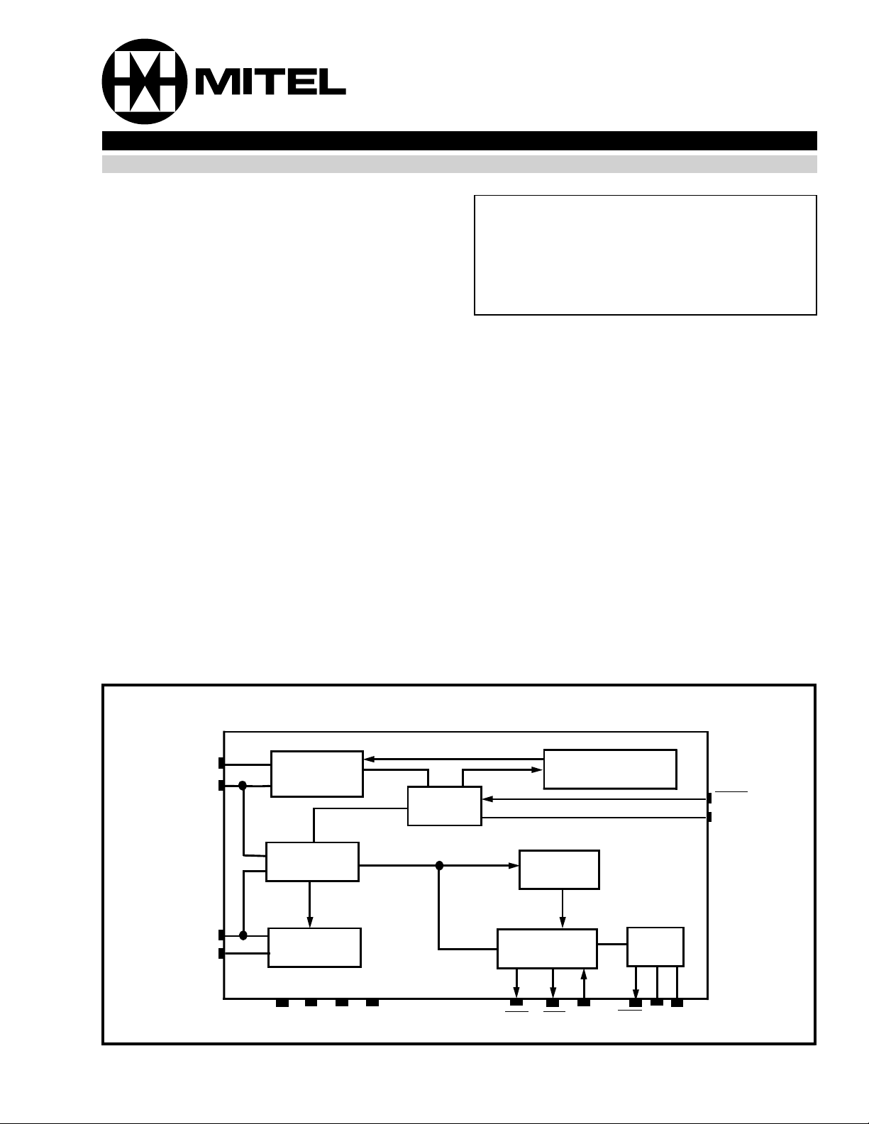
The Mitel MH88510/11 Subscriber Line Interface
Circuit provides a complete interface between the
telephone line and a speech switch requiring only
single bidirectional switch per crosspoint. The
functions provided by the MH88510/11 include
bidirectional differential to single ended conversion
in the speech path, line battery feed, ringing feed
and loop and dial pulse detection. The device is
fabricated as a thick film hybrid which incorporates
various technologies for optimum circuit board and
very high reliability.
TF
TIP
RING
RF
VBAT
Tip
Drive
2-2 Wire
Hybrid
Current &
Voltage
Sensing
Ring Short
Protection
AGND
VDD VEE
Figure 1 - Functional Block Diagram
Ring Trip
Line
Super vi si on
SHK
Current/Vo lt age
Filter
RRC
LED
Constant
Control
RRD
Relay
Driver
VRLY
MUTE
JUNC
RGND
2-53
Page 2
MH88510/11 Preliminary Information
TIP
VDD
RING
RF
TF
VBAT
AGND
VEE
LED
SHK
IC
VDD
AGND
VBAT
MUTE
JUNCTOR
RRD
1
2
3
4
5
6
7
8
9
10
11
12
13
14
15
16
17
18
19
20
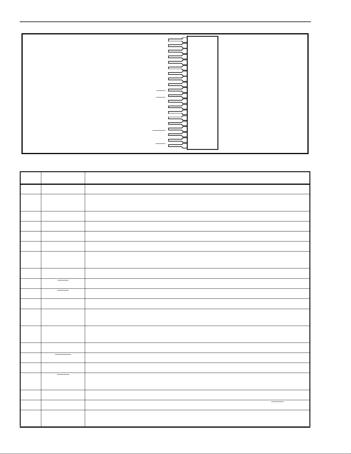
Figure 2 - Pin Connections
Pin Description
Pin # Name Description
1TIPTip Lead. Connects to the “Tip” lead (A-wire) of the telephone line .
2VDDPositive Power Supply Voltage. Normally +5V. This provides current for both internal
circuitry as well as the loop. Not internally connected to pin 12.
3 RING Ring Lead. Connects to the “Ring” lead (B-wi re) of the telephon e line.
4RFRing Feed. Connect t o the Ring Relay contact. See Figure 5.
5 TF Leave open circuit
6 VBAT Battery Voltage Supply. Normally -24V or -48V. Not internally connected to pin 14.
7AGNDAnalog Ground. Supply and batte ry ground. Internally conne cted to pin 13. For
optimum perform ance connect pin 7 to pin 13.
8V
EE
9LED
10 SHK
Negative Pow er Su pp ly Voltage. Normally -5V.
LED Drive (Output). Drives an LED directly. A logic low indicates an off-hook condition.
Switch Hook Detect (Output). A logic low indicate s an off-hook condition.
11 IC Internal Connection . This pin is connected internally
12 V
DD
Positive Power Supply Voltage. Normally +5V. This provides current for both internal
circuitry as well as the loop.
13 AGND Analog Gro und. Supply and battery ground. Internally connected to pin 13. For
optimum perform ance connect pin 13 to pin 7.
14 V
BAT
15 MUT E
Battery Voltage Supply. Normally -24V or -48V. Not internally connected to pin 6.
MUTE (Input). A logic low will mute signals coming from Tip-Ring to the JUNC.
16 JUNC Recei ve/ trans mit aud io speech path. (Referen ced to 0V GND).
17 RRD
Ring Relay Drive (Outpu t). Connects to the ring relay coil. A logic low activates the
relay.
18 RGND Relay Gro und . Return path for relay supply votlage. Normally connected to AGND.
19 RRC Ring Relay Control (Input). A logic high activates the Ring Relay Drive (RRD
) outputs.
20 VRLY Relay Positi ve Supply Voltage. Normally +5V. Connects to the relay coil and the relay
supply voltage. An internal clamp diode from VR LY to RGND is provided.
2-54
Page 3
Preliminary Information MH88510/11
Functional Description
The BORSH Functions
The MH88510/11 performs all of the Borsh functions
of Battery Feed, Overvoltage Protection, Ringing,
Supervision and Hybrid (2-2 Wire).
Battery Feed
The MH88510/11 powers the telephone set with
constant DC loop current for shortlines and
automatically reverts to constant voltage for long
lines. Since the Tip drive is powered down from the
supply, loop current flows through both the V
V
DD
BAT
supply and the VDD supply.
Overvoltage Protection
The MH88510/11 is protected from short ter m (20ms)
transients (+250V) between Tip and Ring, Tip and
ground, and Ring and Ground. However additional
protection circuitry may be needed depending on the
requirements which must be met. Normally, simple
external shunt protection as shown in Figures 5 and
6 is all that is required.
switches ringing voltage on to the line via the
external ring relay. The SLIC provides two internal
300W battery feed resistors through which the
ringing current will flow. A clamp diode is included
which suppresses voltage transients during relay
switching caused by the relay coil. In addition, the
circuit prevents connection of the ringing source
during off-hook conditions. See figure 5 for typical
application.
Hybrid
The 2-2 Wire hybrid circuit converts the incoming
balanced signal at Tip and Ring of the telephone line
into a ground referenced output signal at JUNC of
the SLIC, and converts the ground referenced input
signal at JUNC of the SLIC into a non-balanced
output signal at Tip and Ring of the telephone line.
Line Impedance
The MH88510/11’s Tip-Ring(Zin) impedance is fixed
at 600Ω. For correct SLIC impedance, JUNC must
be appropriately terminated. See AC Electrical
Characteristics.
Supervision
Ringing
The ringing insertion circuitry has the capability to
provide ringing voltage to the telephone set by
simply adding an external relay, ring generator and a
200Ω limiting resistor. The internal relay driver
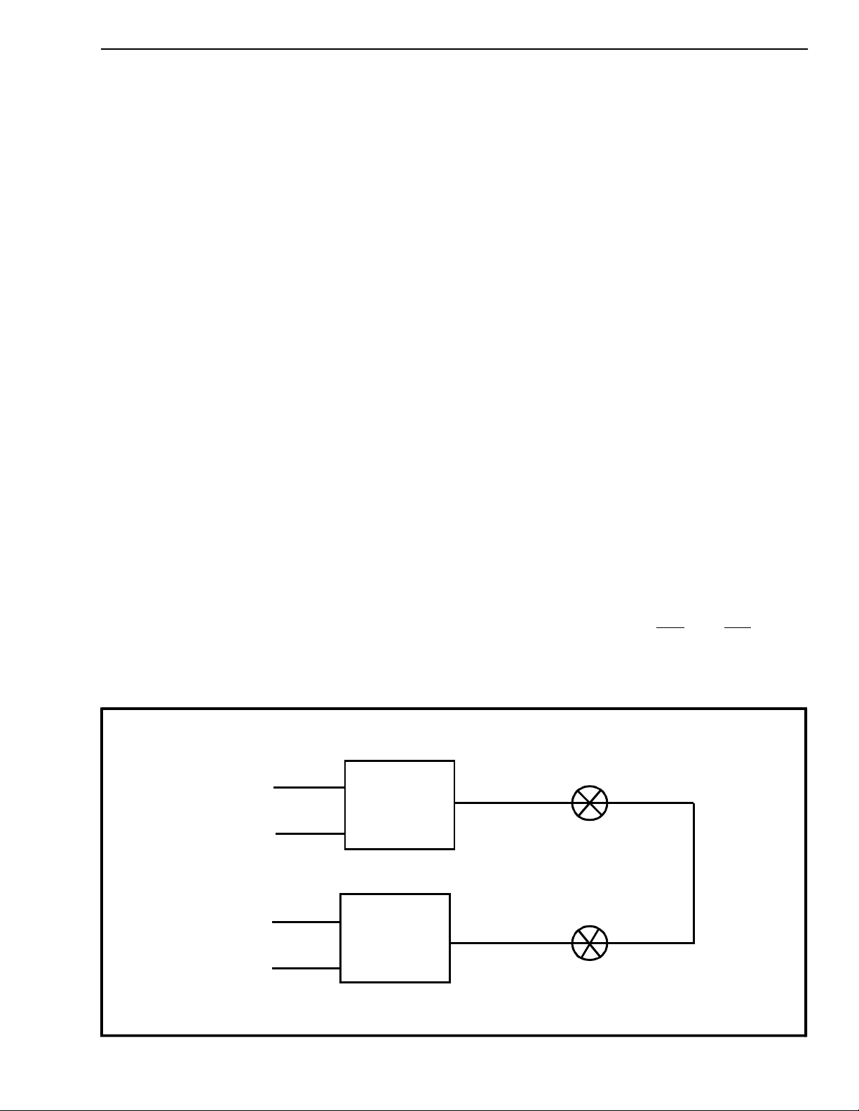
MH88510/11
SLIC 1
TIP
RING
TIP
RING
1
TIP
3
RING
1
TIP
3
RING
JUNC
MH88510/11
SLIC 2
JUNC
The loop detection circuit determines whether a low
enough impedance is across Tip and Ring to be
recognised as an Off-Hook condition. When an offhook condition occurs, the SHK
and LED outputs
toggle to a logic low level. These outputs also toggle
during incoming dial pulses.
75Ω
16
CROSSPOINT
SWITCH
75Ω
16
CROSSPOINT
SWITC H
Figure 3 - SLIC Crosspoi nt S witc h Connecti on
2-55
Page 4

MH88510/11 Preliminary Information
The SHK output has low drive capability while the
output can drive an LED directly. The detection
LED
circuit engages a ringing filter during applied ringing.
The ringing filter ensures that the SHK
at the ringing cadence and not at the ringing
frequency. The ring trip detection circuit also
prevents false off-hook detection due to the current
associated with the AC ringing voltage as well as
current transients when the ringing votlage is
switched in and out.
output toggles
Hybrid
The 2- wire hybrid circuit converts the incoming
balanced signal at Tip and Ring of the telephone line
into a ground referenced output signal at JUNC of
the SLIC, and converts the ground referenced input
signal at JUNC of the SLIC into a non-balanced
output signal at Tip and Ring of the telephone line.
Return Loss at Tip-Ring
To maximise return loss, the impedance at Tip-Ring
should match the SLIC’s impedance (600Ω).
However, the SLIC’s input impedance is dependent
on the JUNC termination resistance. For a 600Ω
SLIC input impedance, the JUNC must be
terminated with 754Ω.
Figure 2 illustrates a typical connection between two
SLICs through two crosspoint switches. Optimum
return loss occurs when JUNC is terminated with
754Ω. Since the JUNC input/output is 604Ω and the
crosspoint switches resistance are 75Ω + 75Ω, this
configuration gives optimum return loss as shown in
Figure 3.
In addition, the Tip-Ring Drive Circuit has the
capability to drive a dry line (a line with no DC
current flowing); the AC Electrical Characteristics
apply (except for longitudinal balance), even when
the loop current drops to zero. Therefore, the
MH88510 has the capability to drive a line much
longer than 2000Ω providing the user is not
concerned with loop current, SHK detection or
ringing generator current.
Short Circuit Protection
The MH88510 is protected from long term (infinite)
short circuit conditions occurring between Tip and
Ring, Tip and AGND, and Ring and AGND.
Line Impedance
The MH88510’s Tip-Ring (Zin) impedance is fixed at
600Ω. For correct SLIC impedance, JUNC must be
appropriately terminated. See AC Electrical
Characteristics.
Transmit and Receive Gain
Transmit Gain (JUNC to Tip-Ring) and Receive Gain
(Tip-Ring to JUNC) are fixed. For correct gain, the
SLIC input impedance must match the line
impedance and JUNC must be appropriately
terminated.
MUTE
A logic low at the MUTE input results on, muted
signals coming from Tip and Ring to the JUNC
terminal while allowing signals from the JUNC
terminal to Tip and Ring to be transmitted.
Tip-Ring Drive Circuit
The audio input ground referenced signal at JUNC is
converted to a differential output signal at Tip and
Ring. The output signal consists of the audio signal
superimposed on the DC battery feed current. The
Tip-Ring drive circuit is optimsed for good 2-Wire
longitudinal balance.
2-56
Page 5

Preliminary Information MH88510/11
TYPICAL
RETURN
LOSS
(dB)
10
20
30
40
50
60
550
600 650
700 750
800
850 900
LOAD IMPEDANCE ON JUNCTOR (Ω)
Figure 4 - Return Loss VS Junctor Lo ad I mped ance
950
TIP
RING
RINGING
GENERATOR
90VRMS
Notes:
R1= 200Ω, 1/4W, 5%
K1= Relay E/M 5V, 1 form C
C1, C2 = 0.1uF, 50V, Ceramic
OPTIONAL
PROTECTION
CIRCUIT
K1
R1
~
-48V
1
3
4
6,14
-5V
MH88510/11
TIP
RING
RF1
VBAT
AGND VDD RGND
VEE
813 12
C1 C2
+5V
JUNC
MUTE
SHK
LED
RRC
RRD
VRLY
18
16
15
10
19
17
20
AUDIO
INPUT/OUTPUT
MUTE CONTROL
INPUT
SWITCH HOOK
OUTPUT
9
DS1
K1
OFF-HOOK LED
RING CONTROL
INPUT
Figure 5 - Typical Applicati on Circuit
2-57
Page 6

MH88510/11 Preliminary Information
Absolute Maximum Ratings
†
Parameter Symbol Min Max Units
1 DC Supply Voltage V
2 DC Battery Voltage V
3 DC Relay Voltage V
V
DD
EE
BAT
RLY
-0.3
0.3
15
-15
0.3 -60 V
-0.3 20 V
4 A C Ring Generator Voltage 150 V
5 S torage Temperature T
† Exceeding these values may cause permanen t damage . Function al operation under these condition s is not implied.
Characteristics Sym Min Typ
1 DC Supply Voltage V
2 DC Battery Voltage V
3 DC Relay Vol tage V
V
DD
EE
BAT
RLY
4.75
-4.75
-23 -48 -56 V
4 AC Ring Generator Voltage
S
‡
5.0
-5.0
5.0 15 V
90 105
Ringing Generator Frequency 17
5 Operating Temperat u re T
‡ Typical figures are at 25°C with nominal+
DC Electrical Characteristics
5V supplies and are for design aid only: not guaranteed and not subject to product ion testi ng.
†
Characteristics Sym Min Typ
OP
070°C
‡
Max Units Test Conditions
-55 125 °C
Max Units Test Conditions
7.35
-8.40
33
V
V
V
RMS
Hz
V
V
RMS
1 Supply Current: Open Loop
Normal Loop
Short Loop
2 Power Consumption①: Open Loop
Normal Loop
Short Loop
3 Low Level Output Voltage ②
High Level Output Voltage
4 Sink Current, LED
Sink Current, LED
to AGND ②
to VDD
5 Sink Current, Relay to VDD
Clamp Diode Current
6 High Level Input Voltage ③
7 Low Level Input Voltage ④
† DC Electrical Characteristics are over recommended operating conditions with V
‡ Typical figures are at 25°C with nominal+
① Supply Current and Power Consumption characteristics are over recommended operating conditions with VDD at 5.0V, VEE at -5.0V and V
loop current flows through both the V
out put consists of a 100kΩ resistor in series with an op-amp with a minimum output voltage swing of ±3.25V.
② SHK
③ LED
outputs consists of a 2.5kΩ resistor in series with SHK op-amp output.
RRC input consists of a 5kW resistor in series with the base lead of the relay driver transistor (grounded emitter).
④ The MUTE
input is internally pulled up. With no input connection, the voltage level at the MUTE input is typically at 1.5V.
5V supplies and are for design aid only: not guaranteed and not subject to production testing.
and the VDD suppl y.
BAT
I
I
I
BAT
I
I
I
BAT
I
I
I
BAT
PC
PC
PC
V
V
I
I
I
I
V
V
DD
EE
DD
EE
DD
EE
OL
OH
OL
OH
OL
CD
15
15
15
43
15
43
43
15
43
880
2360
2360
-3.0
3.0
0.6
2.5
100
mA
R
LOOP
mA
mA
mA
R
LOOP
mA
mA
mA
R
LOOP
mA
mA
mW
mW
mW
V
V
R
LOOP
R
LOOP
R
LOOP
IOL = 2µA
= 2µA
I
OH
mAmAVOL = -1.5V
= 3.25 V
V
OL
mAmAVOL = 0.35V
150
IH
IL
3.5 V
0.8 V
at +5.0V and VEE at -5V ± 5% unless otherwise stated.
DD
IIL = 1.0mA
IIL = 0.5mA
= Open
= 1000Ω
= 0Ω
= Open
= 1000Ω
= 0Ω
at -48V. Note that
BAT
2-58
Page 7

Preliminary Information MH88510/11
AC and DC Loop Electrical Characteristics*
Characteristics Sym Min Typ
1 Maximum AC Ringing
44 mA
‡
Max Units Test Conditions
Current Rejection ①
2 Ring Trip Detect Time 125 ms
3 Operating Loop Current
= -48V
V
BAT
= -23V
V
BAT
4 Maximum Operating Loop
Resistance ② V
BAT
V
BAT
= -48V
= -23V
5 Loop Current at
Off-Hook Detect Threshold
* AC and DC Loop Electrical Characteristics are over recommended operating conditions unless otherwise stated.
‡ Typical figures are at 25°C with nominal + 5V supplies and are for desig n aid only.
① The SLIC can be loaded with an AC impedance as low as 2200Ω without generating a false SHK
the SLIC can drive a REN of 3.6 without generating a false SHK output.
② See section on Tip-Ring Drive Circuit for driving longer lines.
I
IP
R
IP
I
SH
18
18
2000
600
8
9
23
23
10
11
28
28
12
13
mAmAR
Ω
Ω
R
I
Loop
I
Loop
Loop
Loop
< 2000Ω
< 600Ω
= 18mA
= 18mA
µAµAVDD = 5.0V, VEE = -5.0V
= 7.0V, VEE = -8.0V
V
DD
output. Since each REN represents 8kΩ,
AC Electrical Characteristics
Characteristics Sym Min Typ
1 Return Loss at 2-Wire 20 30 dB Reference 600Ω
‡
Max Units Test Conditions
@ 1kHz
2 Impedance at Junctor 604 Ω
3 Longitudinal to Metallic Balance 50 60 dB 40Hz - 4kHz
4 Longitudinal to Junctor Balance 50 60 dB 40Hz - 4kHz
5 Signal Output Overload Level
at Junctor
6 Total Harmonic Distortion
at Junctor
7 Idle Channel Noise
at Junctor
8 Power Supply Rejection Ratio at
at 2-Wire
at 2-Wire
at 2-Wire
THD
Nc
PSRR
3.5
3.5
1.0
1.0
12
12
dBm
dBm
%
%
dBrnc
dBrnc
% THD <
Reference: 600Ω
Reference: 754Ω
Input 0.5V 1kHz
Reference: 600Ω
Reference: 754Ω
Ripple 0.1V 1kHz
5%
2-Wire and Junctor
V
DD
V
EE
V
BAT
25
25
25
dB
dB
dB
9 Mute Attenuation 30 dB Input 0.5V MUTE
= 0.0V @1kHz
‡ Typical figures are at 25°C with nominal + 5V supplies and are for desig n aid only.
2-59
Page 8

MH88510/11 Preliminary Information
AC Gains Table - MH88510
‡
Characteristics Sym Min Typ
Max Units Test Conditions
1 Gain 2-Wire to Junctor 1.05
0.42
2 Frequency Response Gain
-0.3 0.3 dB 200Hz - 3400Hz
(relative to gain at 1kHz)
3 Gain Junctor to 2-Wire 0.96
-0.35
4 Frequency Response Gain
-0.3 0.3 dB 200Ηz - 34 00Hz
(relative to gain at 1kHz)
‡ Typical figures are at 25°C with nominal + 5V supplies and are for design aid only.
AC Gains Table - MH88511
†
Characteristics Sym Min Typ
1 Gain 2-Wire to Junctor 1.15
0.21
2 Frequency Response Gain
-0.3 0.3 dB 200Hz - 3400Hz
(relative to gain at 1kHz)
3 Gain Junctor to 2-Wire 1.04
0.34
4 Frequency Response Gain
-0.3 0.3 dB 200Hz - 3400Hz
(relative to gain at 1kHz)
1.12
0.98
1.00
0.0
1.19
1.50
1.08
0.67
1.19
1.51
1.04
0.35
‡
Max Units Test Conditions
1.22
1.72
1.11
0.91
V/V
dBV
V/V
dBV
V/V
dBV
V/V
dBV
Input 0.5V 1 k Hz
Input 0.5V 1 k Hz
Input 0.5V 1 k Hz
Input 0.5V 1 k Hz
Input 0.5V 1 k Hz
Input 0.5V 1 k Hz
Input 0.5V 1 k Hz
Input 0.5V 1 k Hz
† AC Electrical Characteristics are over recommended operating conditions unless otherwise stated.
‡ Typical figures are at 25°C with nominal +
Note1: All of the above test conditions use 754Ω connected betwe en JUNC and GRD, and 600W connected betwee n Tip and Ring unless
otherwise stated.
Note 2:All of the above test conditions use 200Hz to 6400Hz unless otherwise stated.
Notes
RV1,2,3 = 175VAC, 225VAC, 15J
GE V175LA2 or similar
5V supplies and are for design aid only.
PROTECTION CIRCUIT
TIP
RV2
RV3
RV1
RING
EARTH GROUND SYSTEM
3
TIP
RING
MH88510/11
AGND
7
GROUND
1
2-60
Figure 6 - Ty pical Protection Circuit
Page 9

Preliminary Information MH88510/11
MH88511
J
1
T
D1
D2
R
3
COMPONENTS
D1,D2,=IN4732
D3,D4,D5,D6,D7=IN4003
D8=IN4148
D9=IN5246B
VAR1,VAR2,VAR3-V130LA20A
C1,C3=10µF,60V,5%
C2=1.0µF,100V,5%
C4=0.1µF,100V,5%
C5=0.01µF,100V,5%
C6=0.33µF,200V,5%
R1=1/4W,1%,6.8k
R2,R5=1/4W,10%,10k
T1
C1
Q3
R7
LINE SEIZE
C2
C3
Q1
Q2
R3
C4
D3
D4
D6
D5
D7
R1
R2
R3=1/2W,10%,50Ω
R4=1/4W,10%,680Ω
R6=1/4W,10%,100kΩ
R7=1/4W,10%,1kΩ
R8,R9=1/2W,10%,10Ω
Q1=MPSA90
Q2=ZN6716
Q3=BC238
T1=FILTRAN TPF712 (o r EQU IVALENT) 60 0Ω:1
D8
RELA Y
C5
TIL111
C6
D9
R4
R5
2
1
+5V
VAR1
TIP
R9
VAR2
+5V
R6
RING
DET
5
6
4
V AR3
R8
RING
Figure 7 - M H88511 as a Trunk Interfac e Ap plicati on
MH88510
1dB -2dB 0dB
0dB 1dB -1dB -1dB
MT8816
MH88510
Figure 8a - Line to Line
2-61
Page 10

MH88510/11 Preliminary Information
C.O.
0dB -0.2dB
Side View
T1
-0.2dB
MH88511
1dB -2dB 0dB
1.2dB -0.7dB -0.7dB
MT8816
MH88510
Figure 8b - Li ne to Lin e
0.080 Ma x
(2.0 Max)
2.00 + 0.020
0.5)
(50.8 +
0.010 +
(0.25 +
Notes:
1) Not to scale
2) Dimensions in inches).
3) (Dimensions in millimetres).
*Dim ension s to cen tre of pi n &
tolerance non accumulative.
0.00 2
0.05)
0.02
0.58+
1 2 3 4 19 20
0.5)
(14.7+
0.12 Max
(3.1 Max)
0.01
0.05 +
0.5)
(1.3 +
0.05 +
(1.3 +
Figure 9 - Mechanical Data
0.02
0.18 +
(4.6 +
***
0.02
0.05)
0.020 +
(0.51 +
0.05
0.13)
0.100 +
(2.54 +
0.10
0.13)
0.5)
2-62
 Loading...