

Page 1
Order this document By MCH12140/D
The MCH/K12140 is a phase frequency-detector intended for
phase-locked loop applications which require a minimum amount of phase
and frequency difference at lock. When used in conjunction with the
MC12147, MC12148 or MC12149 VCO, a high bandwidth PLL can be
realized. The device is functionally compatible with the MC12040
phase-frequency detector, however the MOSAIC III process is used to
push the maximum frequency to 800 MHz and significantly reduce the dead
zone of the detector. When the Reference (R) and VCO (V) inputs are
unequal in frequency and/or phase, the differential UP (U) and DOWN (D)
outputs will provide pulse streams which when subtracted and integrated
provide an error voltage for control of a VCO.
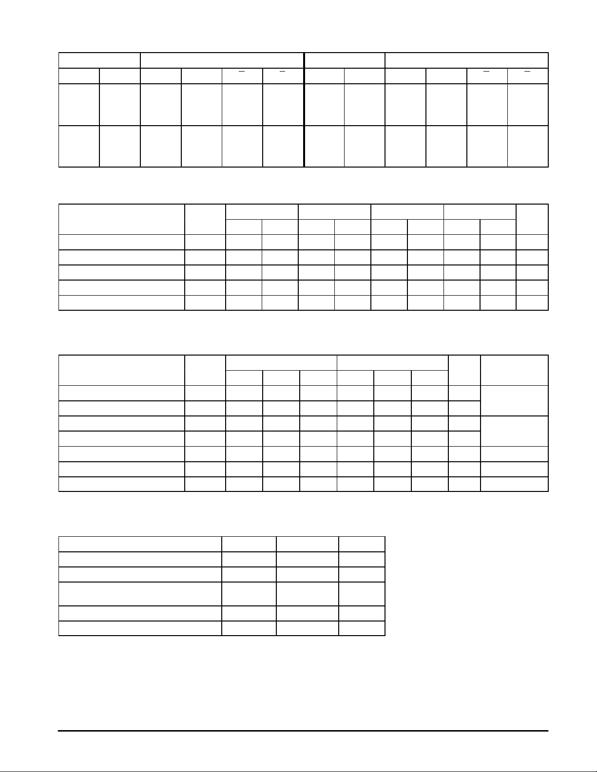
The device is packaged in a small outline, surface mount 8-lead SOIC
package. There are two versions of the device to provide I/O compatibility to
the two existing ECL standards. The MCH12140 is compatible with
MECL10H logic levels while the MCK12140 is compatible to 100K ECL
logic levels. This device can also be used in +5.0 V systems. Please refer to
Motorola Application Note AN1406/D, “Designing with PECL (ECL at +5.0
V)” for more information.
• 800 MHz Typical Bandwidth
• Small Outline 8-Lead SOIC Package
• 75 kΩ Internal Input Pulldown Resistors
• >1000 V ESD Protection
For proper operation, the input edge rate of the R and V inputs should be
less than 5ns.
MOSAIC III and MECL 10H are trademarks of Motorola
PHASE–FREQUENCY
DETECTOR
SEMICONDUCTOR
TECHNICAL DATA
8
1
D SUFFIX
PLASTIC PACKAGE
CASE 751
(SO–8)
PIN CONNECTIONS
R
V
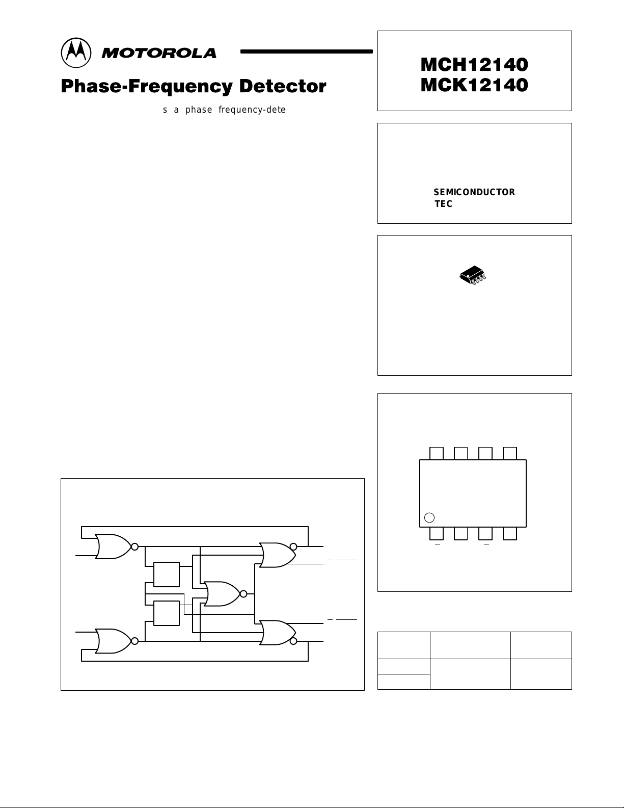
LOGIC DIAGRAM
RQ
S
SQ
R
U (fR > fV)
U
(fR > fV)
D
(fV > fR)
D (fV > fR)
ORDERING INFORMATION
Device
MCH1214OD
MCK12140D
V
R
V
CC
8
7
1
2
U
U
(Top View)
Operating
Temperature Range
TA = –40° to +70°C SO–8
V
EE
6
5
3
4
D
D
Package
Motorola, Inc. 1997 Rev 4
Page 2
MCH12140 MCK12140
TRUTH TABLE*
Input Output Input Output
R V U D U D R V U D U D
0
0
1
0
1
0
1
1
NOTE: * This is not strictly a functional table; i.e., it does not cover all possible modes of operation. However, it gives a sufficient number of tests to ensure that
the device will function properly.
H–SERIES DC CHARACTERISTICS (V
Output HIGH Voltage V
Output LOW Voltage V
Input HIGH Voltage V
Input LOW Voltge V
Input LOW Current I
NOTE: 1.10H circuits are designed to meet the DC specifications shown in the table after thermal equilibrium has been established. The circuit is in a test socket
K–SERIES DC CHARACTERISTICS (V
Output HIGH Voltage V
Output LOW Voltage V
Output HIGH Voltage V
Output LOW Voltage V
Input HIGH Voltage V
Input LOW Voltge V
Input LOW Current I
NOTE: 1.This table replaces the three tables traditionally seen in ECL 100K data books. The same DC parameter values at VEE = –4.5V now apply across the
ABSOLUTE MAXIMUM RATINGS (Note 1)
Power Supply (VCC = 0V) V
Input Voltage (VCC = 0V) V
Output Current Continuous
Operating Temperature Range T
Operating Range
NOTES: 1. Absolute maximum rating, beyond which, device life may be impaired, unless otherwise specified on an individual data sheet.
2.Parametric values specified at: H–Series: –4.20 V to –5.50 V
3.ESD data available upon request.
0
1
1
1
1
1
1
0
X
X
X
X
1
1
1
1
X
X
X
X
0
0
0
0
X
X
X
X
0
0
0
0
= VEE(min) – VEE(max); VCC = GND1, unless otherwise noted.)
EE
X
X
X
X
1
1
1
1
1
1
1
1
1
0
1
1
0
1
0
1
1
1
0
0
0
0
0
0
0
0
0
1
1
1
1
0
1
1
1
1
1
1
1
1
1
0
0
0
0
1
–40°C 0°C 25°C 70°C
Characteristic Symbol Min Max Min Max Min Max Min Max Unit
OH
OL
IL
or mounted on a printed circuit board and transverse airflow greater than 500lfpm is maintained. Outputs are terminated through a 50Ω resistor to –2.0V
except where otherwise specified on the individual data sheets.
–1080 –890 –1020 –840 –980 –810 –910 –720 mV
–1950 –1650 –1950 –1630 –1950 –1630 –1950 –1595 mV
–1230 –890 –1170 –840 –1130 –810 –1060 –720 mV
IH
–1950 –1500 –1950 –1480 –1950 –1480 –1950 –1445 mV
IL
0.5 — 0.5 — 0.5 — 0.3 — µA
= VEE(min) – VEE(max); VCC = GND1, unless otherwise noted.)
EE
–40°C 0°C to 70°C
Characteristic Symbol Min Typ Max Min Typ Max Unit Condition
OH
OL
OHA
OLA
IL
full VEE range of –4.2V to –5.5V. Outputs are terminated through a 50Ω resistor to –2.0V except where otherwise specified on the individual data
sheets.
Characteristic
Surge
1,2
K–Series: –4.94 V to –5.50 V
–1085 –1005 –880 –1025 –955 –880 mV VIN = VIH(max)
–1830 –1695 –1555 –1810 –1705 –1620 mV or VIL(min)
–1095 — — –1035 — — mV VIN = VIH(min)
— — –1555 — — –1610 mV or VIL(max)
IH
–1165 — –880 –1165 — –880 mV
–1810 — –1475 –1810 — –1475 mV
IL
0.5 — — 0.5 — — µA VIN = VIL(max)
Symbol Rating Unit
EE
I
I
out
A
V
EE
–8.0 to 0 VDC
0 to –6.0 VDC
50
mA
100
–40 to +70 °C
–5.7 to –4.2 V
2
MOTOROLA RF/IF DEVICE DATA
Page 3

MCH12140 MCK12140
DC CHARACTERISTICS (V
Characteristic Symbol Min Typ Max Min Typ Max Min Typ Max Min Typ Max Unit
Power Supply Current HKI
Power Supply Voltage HKV
Input HIGH Current I
= VEE(min) – VEE(max); VCC = GND, unless otherwise noted.)
EE
–40°C 0°C 25°C 70°C
EE
EE
IH
–4.75
–4.20
45
45
–5.2
–5.5
–4.5
–5.5
150 150 150 150 µA
383845455252383845455252384245505258mA
–4.75
–4.20
–5.2
–4.5
–5.5
–5.5
–4.75
–4.20
–5.2
–4.5
–5.5
–5.5
–4.75
–4.20
–5.2
–4.5
–5.5
–5.5
V
AC CHARACTERISTICS (V
Characteristic Symbol Min Typ Max Min Typ Max Min Typ Max Min Typ Max Unit
Maximum Toggle Frequency F
Propagation Delay R to D
to Output R to U
V to D
V to U
Output Rise/Fall Times
Q (20 to 80%)
= VEE(min) – VEE(max); VCC = GND, unless otherwise noted.)
EE
–40°C 0°C 25°C 70°C
MAX
t
PLH
t
PHL
t
t
r
f
800 650 800 650 800 650 800
440
330
330
440
225 100 225 350 100 225 350 100 225 350
320
210
210
320
440
330
330
440
580
470
470
580
320
210
210
320
440
330
330
440
580
470
470
580
360
240
240
360
480
360
360
480
APPLICATIONS INFORMATION
The 12140 is a high speed digital circuit used as a phase
comparator in an analog phase-locked loop. The device
determines the “lead” or “lag” phase relationship and time
difference between the leading edges of a VCO (V) signal
and a Reference (R) input. Since these edges occur only
once per cycle, the detector has a range of ±2π radians.
The operation of the 12140 can best be described using
the plots of Figure 1. Figure 1 plots the average value of U
, D
and the difference between U and D versus the phase
difference between the V and R inputs.
There are four potential relationships between V and R: R
lags or leads V and the frequency of R is less than or greater
than the frequency of V. Under these four conditions the
12140 will function as follows:
Figure 1. Average Output Voltage versus
Phase Difference
Fv > Fr R lags V
–2
–2
–2
π
π
π
–
ππ
–
ππ
–
ππ
U
D
U–D
Fv < FrR leads V
V
OH
VOH – V
OL
2
π
2
π
2
π
2
V
OH
VOH – V
2
VOH – V
2
VOL – V
2
OL
OL
OH
R lags V in phase
When the R and V inputs are equal in frequency and the
phase of R lags that of V the U
D
output will pulse from HIGH to LOW. The magnitude of the
output will stay HIGH while the
pulse will be proportional to the phase difference between the
V and R inputs reaching a minimum 50% duty cycle under a
180° out of phase condition. The signal on D
VCO to decrease in frequency to bring the loop into lock.
V frequency > R frequency
When the frequency of V is greater than that of R the
12140 behaves in a simlar fashion as above. Again the signal
on D
indicates that the VCO frequency must be decreased to
bring the loop into lock.
R leads V in phase
When the R and V inputs are equal in frequency and the
phase of R leads that of V the D
the U
output pulses from HIGH to LOW. The magnitude of the
output will stay HIGH while
pulse will be proportional to the phase difference between the
V and R inputs reaching a minimum 50% duty cycle under a
180° out of phase condition. The signal on U
VCO to increase in frequency to bring the loop into lock.
V frequency < R frequency
When the frequency of V is less than that of R the 12140
behaves in a simlar fashion as above. Again the signal on U
indicates that the VCO frequency must be decreased to bring
the loop into lock.
From Figure 1 when V and R are at the same frequency
and in phase the value of U
– D is zero thus providing a zero
error voltage to the VCO. This situation indicates the loop is
in lock and the 12140 action will maintain the loop in its
locked state.
620
500
500
620
ps
ps
indicates to the
indicates to the
MOTOROLA RF/IF DEVICE DATA
3
Page 4

C
A
E
B
A1
MCH12140 MCK12140
D SUFFIX
PLASTIC PACKAGE
CASE 751-06
(SO–8)
ISSUE T
D
58
0.25MB
1
H
4
e
M
h
X 45
_
q
C
A
SEATING
PLANE
0.10
L
B
SS
A0.25MCB
NOTES:
1. DIMENSIONING AND TOLERANCING PER ASME
Y14.5M, 1994.
2. DIMENSIONS ARE IN MILLIMETER.
3. DIMENSION D AND E DO NOT INCLUDE MOLD
PROTRUSION.
4. MAXIMUM MOLD PROTRUSION 0.15 PER SIDE.
5. DIMENSION B DOES NOT INCLUDE DAMBAR
PROTRUSION. ALLOWABLE DAMBAR
PROTRUSION SHALL BE 0.127 TOTAL IN EXCESS
OF THE B DIMENSION AT MAXIMUM MATERIAL
CONDITION.
MILLIMETERS
DIM MIN MAX
A 1.35 1.75
A1 0.10 0.25
B 0.35 0.49
C 0.19 0.25
D 4.80 5.00
E
3.80 4.00
1.27 BSCe
H 5.80 6.20
h
0.25 0.50
L 0.40 1.25
0 7
q
__
Motorola reserves the right to make changes without further notice to any products herein. Motorola makes no warranty , representation or guarantee regarding
the suitability of its products for any particular purpose, nor does Motorola assume any liability arising out of the application or use of any product or circuit, and
specifically disclaims any and all liability, including without limitation consequential or incidental damages. “T ypical” parameters which may be provided in Motorola
data sheets and/or specifications can and do vary in different applications and actual performance may vary over time. All operating parameters, including “Typicals”
must be validated for each customer application by customer’s technical experts. Motorola does not convey any license under its patent rights nor the rights of
others. Motorola products are not designed, intended, or authorized for use as components in systems intended for surgical implant into the body, or other
applications intended to support or sustain life, or for any other application in which the failure of the Motorola product could create a situation where personal injury
or death may occur. Should Buyer purchase or use Motorola products for any such unintended or unauthorized application, Buyer shall indemnify and hold Motorola
and its officers, employees, subsidiaries, affiliates, and distributors harmless against all claims, costs, damages, and expenses, and reasonable attorney fees
arising out of, directly or indirectly, any claim of personal injury or death associated with such unintended or unauthorized use, even if such claim alleges that
Motorola was negligent regarding the design or manufacture of the part. Motorola and are registered trademarks of Motorola, Inc. Motorola, Inc. is an Equal
Opportunity/Affirmative Action Employer.
How to reach us:
USA/EUROPE/Locations Not Listed: Motorola Literature Distribution; JAPAN: Nippon Motorola Ltd.: SPD, Strategic Planning Office, 141,
P.O. Box 5405, Denver, Colorado 80217. 1–303–675–2140 or 1–800–441–2447 4–32–1 Nishi–Gotanda, Shagawa–ku, Tokyo, Japan. 03–5487–8488
Customer Focus Center: 1–800–521–6274
Mfax: RMFAX0@email.sps.mot.com – TOUCHTONE 1–602–244–6609 ASIA/PACIFIC: Motorola Semiconductors H.K. Ltd.; 8B Tai Ping Industrial Park,
Moto rola Fax Back Sys tem – US & Canada ONLY 1–800–774–1848 51 Ting Kok Road, T ai Po, N.T., Hong Kong. 852–26629298
HOME PAGE: http://motorola.com/sps/
4
– http://sps.motorola.com/mfax/
◊
Mfax is a trademark of Motorola, Inc.
MOTOROLA RF/IF DEVICE DATA
MCH12140/D
 Loading...