

Page 1

Part # Description
M-986-1R2P 40-pin plastic DIP, Single Channel
M-986-1R2PL 44-pin PLCC, Single Channel
M-986-2R2P 40-pin plastic DIP, Dual Channel
M-986-2R2PL 44-pin PLCC, Dual Channel
www.clare.com
DS-M976-2R2-R3
M-986-2R2
MFC Transceivers
1
Block Diagram
Pin Assignments
Ordering Information
Features
• Direct A-Law PCM digital input
• 2.048 Mb/s clocking
• Programmable forward/backward mode
• Programmable compelled/direct control
• Operates with standard codecs for analog
interfacing
• Microprocessor read/write interface
• Binary or 2-of-6 data formats
• Single- or dual-channel versions
• 5 volt power
Applications
• Test equipment
• Trunk adapters
• Paging terminals
• Traffic recorders
• PBXs
Description
The M-986-1R2 and -2R2 MFC Transceivers contain
all the logic necessary to transmit and receive CCITT
R2F (forward) and R2B (backward) multifrequency
signals on one 40-pin integrated circuit (IC). M-9861R2 is a single-channel version; M-986-2R2 provides
two channels. R1 single and dual multifrequency
transceivers are also available as M-986-1R1 and 2R1.
Operating with a 20.48 MHz crystal, the M-986 is
capable of providing a direct digital interface to an Alaw-encoded PCM digital input. Each channel can be
connected to an analog source using a coder-decoder
(codec) as shown in the Block Diagram below.
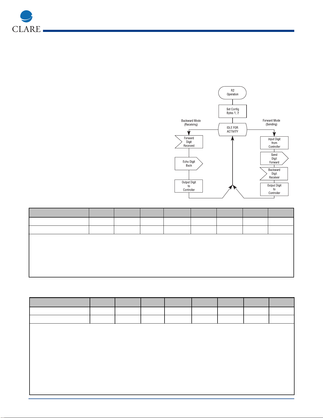
The M-986 can be configured by the customer to
operate with the transmitter and receiver either coupled together or independently, allowing it to handle a
compelled cycle automatically or via command from
the host processor. For the R2 versions of the M-986,
A-law is used for coding/decoding. The M-986 is configured and controlled through an integral coprocessor
port.
Page 2

Configuration Bytes
Configuration Byte 1
Bit 7 Bit 6 Bit 5 Bit 4 Bit 3 Bit 2 Bit 1 Bit 0
0 0 ECLK IOM ENC1 EOD1 CMP1 FB1
ECLK Channels 1 & 2 1 = External codec clock; 0 = Internal codec clock
IOM Channels 1 & 2 1 = Binary input/output; 0 = 2-of-6 input/output
ENC1 Channel 1 1 = Enable channel; 0 = Disable channel
EOD1 Channel 1 1 = Indicate end of digit; 0 = No end of digit indication
CMP1 Channel 1 1 = Automatic Compelled mode; 0 = Manual mode
FB1 Channel 1 1 = Forward mode (Tx forward frequencies and Rx backward frequencies)
0 = Backward mode (Tx backward frequencies and Rx forward frequencies)
Configuration Byte 2
Bit 7 Bit 6 Bit 5 Bit 4 Bit 3 Bit 2 Bit 1 Bit 0
0 1 0 0 ENC2 EOD2 CMP2 FB2
ENC2 Channel 2 1 = Enable channel; 0 = Disable channel
EOD2 Channel 2 1 = Indicate end of digit; 0 = No end of digit indication
CMP2 Channel 2 1 = Automatic Compelled mode; 0 = Manual mode
FB2 Channel 2 1 = Forward mode (Tx forward frequencies and Rx backward frequencies)
0 = Backward mode(Tx backward frequencies and Rx forward frequencies)
www.clare.com
2
M-986-2R2
Rev. 3
Function Description
The M-986 can be set up for various operating modes
by writing two configuration bytes to the coprocessor
port.
Configuration Options
External/Internal Codec Clock (ECLK): If external
codec clocking is selected, an external clocking source
provides an 8kHz transmit framing clock and an 8kHz
receive framing clock. It also provides a serial bit clock
with a frequency that is a multiple of 8 kHz between
2.496 MHz and 216 kHz for exchange of data via the
serial ports. When internal codec clocking is selected,
the M-986 provides an 8kHz framing clock and a 2.048
MHz serial bit clock.
Binary/2 of 6 Input/Output (IOM): When the 2-of-6
input/output is selected, the M-986 encodes the
received R2 MF tone pair into in a 6-bit format, where
each bit represents one of the six possible frequencies.
A logic high level indicates the presence of a frequency. The digital input to the M-986 that selects the transmitted R2 MF tone pair must also be coded in the
2-of-6 format.
When binary input/output is selected, the M-986
encodes the received R2 MF tone pair into a 4 bit binary format. The digital input to the M-986 that selects the
transmitted R2 MF tone pair must also be coded in a 4
bit binary format.
Enable/Disable Channel (ENC): When a channel is
disabled, the receiver does not process its codec input
for R2 MF tones, and the transmitter does not respond
to transmit commands. If a transmit command is given
while the channel is enabled, the “tone off” command
must be given before the channel is disabled.
Disabling the channel does not automatically shut off
the transmitter. When a channel is enabled, the receiver and transmitter for that channel function normally.
End-of-Digit Indication (EOD): The end-of-digit indication option configures the M-986 to inform the host
processor when the far end terminates transmission of
the R2 MF tone it is sending. If this option is disabled,
the host processor will not be notified when tone
transmission terminates.
Automatic Compelled/Manual Sequence Signaling
(CMP): When manual mode is selected, R2 MF tone
transmission is turned on and off only via command
from the host processor.
If the automatic mode is selected, the transmitter and
receiver perform the compelled signaling handshake
automatically. The specifics of operation are different
for the forward and backward configurations.
In forward mode, the transceiver can exist in two
states, STATE 1 and STATE 2:
• STATE 1: No backward signal detected.
Transmitter under control of the host.
• STATE 2: Backward signal detected.
Transmitter off unconditionally.
Page 3
M-986-2R2
www.clare.com
3
Rev. 3
A Transmit Tone Command written while the transceiver is in STATE 1 will be acted upon immediately. The
transmitter is unconditionally disabled upon entry into
STATE 2. If a transmit command is written to the transceiver while in STATE 2, that command will become
pending. Upon entry into STATE 1, a pending transmit
command is acted upon.
In backward mode, the transceiver can exist in two
states, STATE 1 and STATE 2:
STATE 1: No forward signal detected.
Transmitter off unconditionally.
STATE 2: Forward signal detected.
Transmitter transmits backward signal.
A transmit tone command written while the transceiver
is in STATE 2 will be acted upon immediately. The
transmitter is unconditionally disabled upon entry into
STATE 1. If a transmit command is written to the transceiver while in STATE 1, that command will become
pending. Upon entry into STATE 2, a pending transmit
command is acted upon.
EXAMPLE: Assume that the transceivers at both ends
of a link are configured in automatic compelled mode.
Both transceivers are in STATE 1. A compelled signaling sequence begins with the R2F host writing a transmit command byte to its transceiver via the
coprocessor bus. The transceiver immediately begins
transmitting the signal.
Automatic Compelled Mode Operation
Binary Coding Format
Byte Bit 7 Bit 6 Bit 5 Bit 4 Bit 3 Bit 2 Bit 1 Bit 0
Transmit tone command 1 CHN 0 0 A B C D
Receive tone return 0 CHN 0 0 A B C D
CHN: 1 = channel 2; 0 = channel 1
R2 MF Frequencies:
ABCD Forward (Hz) Backward (Hz) ABCD Forward (Hz) Backward (Hz)
0 0 0 0 Tone off Tone off 1 0 0 0 1500 & 1860 1020 & 660
0 0 0 1 1380 & 1500 1140 & 1020 1 0 0 1 1620 & 1860 900 & 660
0 0 1 0 1380 & 1620 1140 & 900 1 0 1 0 1740 & 1860 780 & 660
0 0 1 1 1500 & 1620 1020 & 900 1 0 1 1 1380 & 1980 1140 & 540
0 1 0 0 1380 & 1740 1140 & 780 1 1 0 0 1500 & 1980 1020 & 540
0 1 0 1 1500 & 1740 1020 & 780 1 1 0 1 1620 & 1980 900 & 540
0 1 1 0 1620 & 1740 900 & 780 1 1 1 0 1740 & 1980 780 & 540
0 1 1 1 1380 & 1860 1140 & 660 1 1 1 1 1860 & 1980 660 & 540
2 of 6 Coding Format
Byte Bit 7 Bit 6 Bit 5 Bit 4 Bit 3 Bit 2 Bit 1 Bit 0
Transmit tone command 1 CHN F6 F5 F4 F3 F2 F1
Receive tone return 0 CHN F6 F5 F4 F3 F2 F1
CHN: 1 = channel 2; 0 = channel 1
R2 MF Frequencies:
Bit name Forward (Hz) Backward (Hz) Bit name Forward (Hz) Backward (Hz)
F6 1980 540 F3 1620 900
F5 1860 660 F2 1500 1020
F4 1740 780 F1 1380 1140
Page 4

www.clare.com
4
M-986-2R2
Rev. 3
The R2B transceiver detects the signal, enters STATE
2, and outputs the received tone code to its host via the
coprocessor port. If the R2B host had determined the
next tone to transmit and written a transmit command
to the transceiver prior to entry into STATE 2, the state
transition will cause this tone to be transmitted.
Otherwise, the R2B transmitter waits for a transmit
tone command from the host, and starts transmitting a
tone once the transmit tone command is received.
The R2F transceiver detects the backward signal,
enters STATE 2, and outputs the received tone code to
its host. Entry into STATE 2 unconditionally disables
the transmitter.
The R2B transceiver detects the absence of signal,
enters STATE 1, and informs the host with the end-oftone code if configured to do so. Entry into STATE 1
unconditionally disables the transmitter.
The R2F transceiver detects the absence of signal,
enters STATE 1, and informs the host with the end-oftone code if configured to do so. If the R2F host had
determined the next signal to transmit and written a
transmit command to the transceiver prior to entry into
STATE 1, the state transition will cause this signal to be
transmitted. Otherwise, the transmitter remains silent
until the next transmit command by its host.
Forward/Backward Frequencies (FB): When forward
mode is selected, the R2F (forward) frequencies are
transmitted and R2B (backward) frequencies are
received. When backward mode is selected, R2B frequencies are transmitted and R2F frequencies are
received. The R2F frequencies are 1380, 1500, 1620,
1740, 1860, and 1980 Hertz. The R2B frequencies are
540, 660, 780, 900, 1020, and 1140 Hz.
Initial Configuration: The configuration of the M-986
immediately after a reset will be as follows:
· End-of-digit indication ON
· Forward mode ON
· Channel disabled
· 2-of-6 input/output
· External serial and serial frame clocks.
Also, the M-986 will place 00 hex on the coprocessor
port to indicate to the host processor that it is working.
Transmit Tone Command
The transmit tone command allows the host processor
to transmit any two of the 6 possible frequencies in the
transmission mode the channel has been configured
for (forward or backward). The format of the command
depends on whether the M-986 is configured for binary format or 2-of-6 format.
Recieved Tone Detection
When a tone is detected by the M-986, the TBLF output goes low, indicating reception of the tone to the
host processor. The host processor can determine
which tone was detected and which channel the tone
was detected on by reading data from the M-986
coprocessor port. The M-986 will return a single byte
indicating the tone received and the channel that the
tone was received on.The format of the returned byte
depends on whether the M-986 is configured for binary or 2-of-6 coding.
Coprocessor Port
Commands are written to the M-986 via the coprocessor port, and data indicating the received R2 MF tone
is read from the coprocessor port.
Writing to the Coprocessor Port: The following
sequence describes writing a command to the M-986.
(1) The WR signal is driven low by the host processor.
(2) The RBLE (receive buffer latch empty) signal transitions to a logic high level.
(3) Data is written from LD7-LD0 to the receive buffer
latch (D7-D0) when the WR signal goes high.
(4) The RBLE signal transitions to a logic low level after
the M-986 reads the data. This signals the host
processor that the receive buffer is empty.
Note: The RBLE should be low before writing to the
coprocessor.
Reading the Coprocessor Port: The following
sequence describes reading received tone information
from the coprocessor port.
(1) The TBLF (transmit buffer latch full) port pin on the
M-986 goes low indicating the reception of a tone.
(2) The host processor detects the low logic level on
the TBLF pin either by polling a connected port pin or
by an interrupt.
(3) The host processor drives the RD signal low.
(4) The TBLF (transmit buffer latch full) signal transitions to a logic high level.
(5) Data is driven onto LD7-LD0 by the M-986 until the
RD signal is driven high by the host processor.
Clock Characeristics and Timing
Internal Clock Option: The internal oscillator is enabled
by connecting a crystal across X1 and X2/CLKIN. The
crystal must be 20.48 MHz, fundamental mode, and
parallel resonant, with an effective series resistance of
30 ohms, a power dissipation of 1 mW, and bespecified at a load capacitance of 20 pf.
Page 5

Signal Description
Signal DIP PLCC I/O/Z Description
Pinout Pinout
Note: Please see the following definitions: DIP = Dual In-line Package PLCC = Plastic Leaded Chip Carrier
D15-D8 18-11 13-17, 19-21 I/O/Z Unused. Leave open.
D7-D0 19-26 22-28, 30 I/O/Z 8-bit coprocessor latch.
TBLF 40 44 O Transmit buffer latch full flag.
RBLE 1 2 O Receive buffer latch empty flag
HI/LO 2 3 I Latch byte select pin. Tie low.
BIO 9 10 I Unused. Leave open.
RD 32 36 I/O Used by the external processor to read from the coprocessor
latch by driving the RD line active (low), thus enabling the output
latch to drive the latched data. When the data has been read, the
external device must bring the RD line high.
EXINT 5 6 I Unused. Leave open.
MC 3 4 I Microcomputer mode select pin. Tie low.
MC/PM 27 31 I Coprocessor mode select pin. Tie low.
RS 4 5 I Reset input for initializing the device. When an active low is placed
on RS pin for a minimum of five clock cycles, RD and WR are
forced high, and the data bus (D7 through D0) goes to a high
impedance state. The serial port clock and transmit outputs also go
to the high impedance state.
WR 31 35 I/O Used by the external processor to write data to the coprocessor
port. To write data the external processor drives the WR line low,
places data on the data bus, and then drives the WR line high to
clock the data into the on-chip latch.
XF 28 32 O Watchdog signal. Toggles at least once every 15 milliseconds when
the processor is functioning properly. If the pin is not toggled at
least once every 15 ms, the processor is lost and should be reset.
CLKOUT 6 7 O System clock output (one-fourth crystal/CLKIN frequency,
nominally 5.12 MHz).
V
CC
30 34 I 5V supply pin.
V
SS
10 1, 12, 18, 29 I Ground pin.
X1 7 8 O Crystal output pin for internal oscillator. If an internal oscillator is
not used, this pin should be left unconnected.
X2/CLKIN 8 9 I Input pin to the internal oscillator (X2) from the crystal.
Alternatively, an input pin for the external oscillator (CLKIN).
DR1 & DR0 33 & 29 37, 33 I Serial-port receive-channel inputs. 2.048 MHz serial data is received
in the receive registers via these pins. DR0 = channel 1; DR1 =
channel 2
DX1 & DX0 36 & 35 40, 39 O Serial-port transmit-channel outputs. 2.048 MHz serial data is
transmitted from the transmit registers on these pins.These outputs
are in the high-impedance state when not transmitting.
M-986-2R2
www.clare.com
5
Rev. 3
External Clock Option: An external frequency source
can be used by injecting the frequency directly in
X2/CLKIN, with X1 left unconnected. The external frequency injected must conform to the specifications listed in the External Frequency specification Table on
page 7.
Flammability/Reliability Specifications
Reliability: 185 FITS failures/billion hours
Flammability: Passes UL 94 V-0 tests
Page 6

Serial Port Timing
Parameter Min Nom Max Units
td(CH-FR) Internal framing delay from SCLK rising edge - - 70 ns
td(DX1-CL) DX bit 1 valid before SCLK falling edge 20 - - ns
td(DX2-CL) DX bit 2 valid before SCLK falling edge 20 - - ns
th(DX) DX hold time after SCLK falling edge 244 - - ns
tsu(DR) DR setup time before SCLK falling edge 20 - - ns
th(DR) DR hold time after SCLK falling edge 20 - - ns
tc(SCLK) Serial port clock cycle time 399 488.28 4770 ns
tf (SCLK) Serial port clock fall time - - 30 ns
tr(SCLK) Serial port clock rise time - - 30 ns
tw(SCLKL) Serial port clock low-pulse duration* 220 244.14 2500 ns
tw(SCLKH) Serial port clock high-pulse duration* 220 244.14 2500 ns
t
su
(FS) FSX/FSR setup time before SCLK falling edge 100 - - ns
* The duty cycle of the serial port clock must be within 45% to 55%.
Supply voltage range, V
CC
-0.3 V to 7 V
Input voltage range -0.3 V to 15 V
Output voltage range -0.3 V to 15 V
Ambient air temperature range 0°C to 70°C
Storage temperature range -45°C to 150°C
Signal Description (continued)
Signal DIP PLCC I/O/Z Description
Pinout Pinout
FR 37 41 O 8 kHz internal serial-port framing output. If internal clocking is
selected, serial-port transmit and receive operations occur
simultaneously on an active (high) FR framing pulse.
FSR 39 43 I 8 kHz external serial-port receive-framing input. If external clocking
is selected, data is received via the receive pins (DR1 and DR0) on
the active (low) FSR input. The falling edge of FSR initiates the
receive process, and the rising edge causes the M-986 to process
the data.
FSX 38 42 I 8 kHz external serial-port transmit-framing input. If external clocking
is enabled, data is transmitted on the transmit pins (DX1, DX0) on
the active (low) input. The falling edge of FSX initiates the transmit
process,and the rising edge causes the M-986 to internally load data
for the next cycle.
SCLK 34 38 I/O/Z 2.048 MHz serial-port clock. Master clock for transmitting and
receiving serial-port data. Configured as an input in external clocking
mode or output in internal clocking mode. Reset (RS) forces SCLK
to the high-impedance state.
www.clare.com
6
M-986-2R2
Rev. 3
Absolute Maximum Ratings Over Specified
Temperature
Absolute Maximum Ratings are stress ratings. Stresses in
excess of these ratings can cause permanent damage to
the device. Functional operation of the device at these or
any other conditions beyond those indicated in the operational sections of this data sheet is not implied. Exposure of
the device to the absolute maximum ratings for an extended period may degrade the device and effect its reliability.
Page 7

Coprocessor Interface Timing
Parameter Min Nom Max Unit
t
d(R-A)
RD low to TBLF high - - 75 ns
t
d(W-A)
WR low to RBLE high - - 75 ns
t
a(RD)
RD low to data valid - - 80 ns
t
h(RD)
Data hold time after RD high 25 - - ns
t
su(WR)
Data setup time prior to WR high 30 - - ns
t
h(WR)
Data hold time after WR high 25 - - ns
t
w(RDL)
RD low-pulse duration 80 - - ns
t
w(WRL)
WR low-pulse duration 60 - - ns
t
wr(RBLE)
RBLE↑ to RBLE↓ --1ms
Recommended Operating Conditions
Parameter Min Nom Max Unit
V
CC
Supply voltage 4.75 5 5.25 V
V
SS
Supply voltage - 0 - V
V
IH
High-level input voltage All inputs except CLKIN 2 - - V
CLKIN 3 - - V
MC/PM 2.2 - - V
V
IL
Low-level input voltage All inputs except MC/MP - - 0.8 V
MC/MP - - 0.6 V
I
OH
High-level output current (all outputs) - - -300 µA
I
OL
Low-level output current (all outputs) - - 2 mA
External Frequency Specifications
Parameter Min Nom Max Unit
tC(MC) Master clock cycle time 48.818 48.828 48.838 ns
tr(MC) Rise time master clock input - 5 10 ns
t
f
(MC) Pulse duration master clock 20 - - ns
Electrical Characteristics/Temperature Range
Parameter Test Conditions Min Typ Max Unit
I
CC
Supply current f = 20.5 MHz, VCC= 5.5V, - 50 75 mA
TA= 0˚ to 70 ˚C
V
OH
High-level output voltage IOH= MAX 2.4 3 - V
IOH= 20 µ A VCC-0.4 - - V
VOLLow-level output voltage IOL= MAX - 0.3 0.6 V
I
OZ
Off-state output current V
CC
= MAX VO = 2.4 V - - 20 µA
VO = 0.4 V - - -20 µA
I
I
Input current VI = VSSto V
CC
Except CLKIN - - ±20 µA
CLKIN - - ±50 µA
C
I
Input capacitance Data bus f = 1 MHz, all other pins 0 V - 25 - pF
All others - 15 - pF
C
O
Output capacitance Data bus - 25 - pF
All others - 10 - pF
M-986-2R2
www.clare.com
7
Rev. 3
Page 8

Reciever Characteristics
Parameter Test Conditions Min Max Unit
A
d
Detect amplitude Per frequency -35 -5 dBm0
A
nd
No-detect amplitude Per frequency -42 -35 dBm0
F
d
Detect with frequency offset From nominal ±10 - Hz
TW
d
Detect with twist Adjacent frequencies ±5 - dB
Nonadjacent frequencies ±7 - dB
TW
nd
No detect with twist ±20 - dB
T3
r
Third R2F tone reject Relative to highest levelfrequency -20 - dB
FF
d
Detect R2B with R2F disturbing Above lowest level R2B tone
(-12.5 dBm0 max.) 13.5 - dB
FT
nd
No detect R2F with 2 out-of-band sine waves Any frequencies from
330 - 1150 Hz and 2130 - 3400 Hz -5 - dBm0
RT
nd
No detect R2B with 2 out-of-band sine waves Any frequencies from 1300-3400 Hz -5 - dBm0
T
on
Tone time Reject 7 - ms
T
int
Interrupted tone time Reject 7 - ms
T
or
Operate and release time -80
Transmitter Characteristics
Parameter Test Conditions Min Typ Max Unit
F
OS
Frequency offset From nominal - - ±1 Hz
T
W
Twist High/low - - ±0.5 dB
A
S
Signal amplitude Per component -9.26 -8.86 -8.46 dBm0
T
S
Time skew Between components - - 0 ms
P
hi
Power due to harmonic distortion and
intermodulation 300 to 3400 Hz - - -46.5 dBm0
CLKOUT Timing Parameters
Parameter Test Conditions Min Nom Max Unit
t
c(C)
CLKOUT cycle time 195.27 195.31 195.35 ns
t
r(C)
CLKOUT rise time RL= 825 - 10 - ns
t
f(C)
CLKOUT fall time CL= 100 pFΩ -8-ns
t
d(MCC)
Delay time CLKIN↑ to CLKOUT↓ 25 - 60 ns
Reset (RS) Timing
Parameter Test Conditions Min Max Unit
t
dis
(R) Data bus disable time after RS RL= 825 - 75 ns
t
d12
Delay time from RS↓ to high-impedance SCLK CL= 100 pFΩ - 200 ns
t
d13
Delay time from RS↓ to high-impedance DX1, DX0 - 200 ns
tsu(R) Reset (RS) setup time prior to CLKOUT 50 - ns
tw(R) RS pulse duration 977 - ns
www.clare.com
8
M-986-2R2
Rev. 3
Page 9

M-986-2R2
www.clare.com
9
Rev. 3
External Framing Timing Diagrams
Internal Framing Timing
Page 10

www.clare.com
10
M-986-2R2
Rev. 3
Reset Timing
Coprocessor Timing
Page 11

M-986-2R2
www.clare.com
11
Rev. 3
M-986 Dual Channel 4-Wire Interface Circuit
Page 12

Tolerances
(inches) Metric (mm)
Min Max Min Max
A .165 .180 4.191 4.572
A1 .090 .20 2.286 5.08
A2 .062 .083 1.575 2.108
C .020 min .508 min
D .685 .695 17.399 17.653
D1 .650 .653 16.510 16.662
www.clare.com
12
M-986-2R2
Rev. 3
Mechanical Dimensions
Tolerances
(inches) Metric (mm)
Min Max Min Max
A - .250 - 6.35
A1 .015 - .39
B .014 .022 .356 .558
B1 .030 .070 .77 1.78
C .008 .015 .204 .38
D 1.98 2.095 50.30 53.20
E .600 .625 15.24 15.87
E1 .485 .580 12.32 14.73
e .100 BSC 2.54 BSC
L .115 .200 2.93 5.08
Dimensions
mm
(inches)
Page 13

Worldwide Sales Offices
CLARE LOCATIONS
Clare Headquarters
78 Cherry Hill Drive
Beverly, MA 01915
Tel: 1-978-524-6700
Fax: 1-978-524-4900
Toll Free: 1-800-27-CLARE
Clare Switch Division
4315 N. Earth City Expressway
Earth City, MO 63045
Tel: 1-314-770-1832
Fax: 1-314-770-1812
Clare Micronix Division
145 Columbia
Aliso Viejo, CA 92656-1490
Tel: 1-949-831-4622
Fax: 1-949-831-4628
SALES OFFICES
AMERICAS
Americas Headquarters
Clare
78 Cherry Hill Drive
Beverly, MA 01915
Tel: 1-978-524-6700
Fax: 1-978-524-4900
Toll Free: 1-800-27-CLARE
Eastern Region
Clare
603 Apache Court
Mahwah, NJ 07430
Tel: 1-201-236-0101
Fax: 1-201-236-8685
Toll Free: 1-800-27-CLARE
Central Region
Clare Canada Ltd.
3425 Harvester Road, Suite 202
Burlington, Ontario L7N 3N1
Tel: 1-905-333-9066
Fax: 1-905-333-1824
Western Region
Clare
1852 West 11th Street, #348
Tracy, CA 95376
Tel: 1-209-832-4367
Fax: 1-209-832-4732
Toll Free: 1-800-27-CLARE
Canada
Clare Canada Ltd.
3425 Harvester Road, Suite 202
Burlington, Ontario L7N 3N1
Tel: 1-905-333-9066
Fax: 1-905-333-1824
EUROPE
European Headquarters
CP Clare nv
Bampslaan 17
B-3500 Hasselt (Belgium)
Tel: 32-11-300868
Fax: 32-11-300890
France
Clare France Sales
Lead Rep
99 route de Versailles
91160 Champlan
France
Tel: 33 1 69 79 93 50
Fax: 33 1 69 79 93 59
Germany
Clare Germany Sales
ActiveComp Electronic GmbH
Mitterstrasse 12
85077 Manching
Germany
Tel: 49 8459 3214 10
Fax: 49 8459 3214 29
Italy
C.L.A.R.E.s.a.s.
Via C. Colombo 10/A
I-20066 Melzo (Milano)
Tel: 39-02-95737160
Fax: 39-02-95738829
Sweden
Clare Sales
Comptronic AB
Box 167
S-16329 Spånga
Tel: 46-862-10370
Fax: 46-862-10371
United Kingdom
Clare UK Sales
Marco Polo House
Cook Way
Bindon Road
Taunton
UK-Somerset TA2 6BG
Tel: 44-1-823 352541
Fax: 44-1-823 352797
ASIA/PACIFIC
Asian Headquarters
Clare
Room N1016, Chia-Hsin, Bldg II,
10F, No. 96, Sec. 2
Chung Shan North Road
Taipei, Taiwan R.O.C.
Tel: 886-2-2523-6368
Fax: 886-2-2523-6369
http://www.clare.com
Clare, Inc. makes no representations or warranties with respect to
the accuracy or completeness of the contents of this publication
and reserves the right to make changes to specifications and
product descriptions at any time without notice. Neither circuit
patent licenses nor indemnity are expressed or implied. Except as
set forth in Clare’s Standard Terms and Conditions of Sale, Clare,
Inc. assumes no liability whatsoever, and disclaims any express or
implied warranty, relating to its products including, but not limited to, the implied warranty of merchantability, fitness for a particular purpose, or infringement of any intellectual property right.
The products described in this document are not designed,
intended, authorized or warranted for use as components in systems intended for surgical implant into the body, or in other applications intended to support or sustain life, or where malfunction
of Clare’s product may result in direct physical harm, injury, or
death to a person or severe property or environmental damage.
Clare, Inc. reserves the right to discontinue or make changes to its
products at any time without notice.
Specification: DS-M986-2R2-R3
©Copyright 2001, Clare, Inc.
All rights reserved. Printed in USA.
7/20/01
 Loading...