

Page 1
LZ93N61
Timing Pulse Generator LSI for CCD
DESCRIPTION
The LZ93N61 is a CMOS timing generator LSI
which provides timing pulses used to drive a
area sensor, in combination with the SSG
LSI (LZ93NI 9, LZ93B53).
FEATURES
●
320000 pixels CCD
●
●
Internal electronic shutter :
Shutter speed is selectable from 1/W, 1/125,
1/250, 1/500, 1/1 000, 1/2 000, 1/4 000 and
1/10 000 s, in addition to this, 1/100 s (PAL
: 1/120 s) in Flicker-less mode using parallel
or serial code. Shutter speed can also be
controlled in 1 H period using an external
trigger to the EXST input.
Single +5
●
Package : 48-pin
between 270000 pixels
systems
power supply
and
and PAL
01 O)
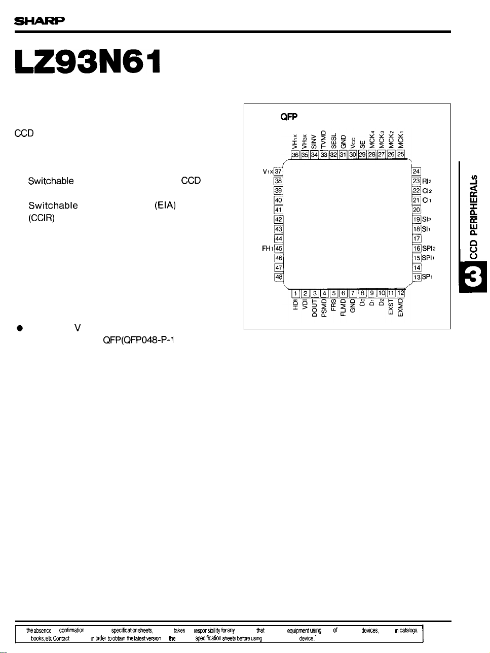
PIN CONNECTIONS
48-PIN
37
V2X 3a
39
V3X
V4X 40
OFDX 41
FR 42
GND 43
FH2 44
CKI 46
CKO 47
TSTI
o
TOP VIEW
24 R12
23
22
21
20 FCDS
19
18
17 FS
16
15
14 SP2
13
“In
deta
of
hn~ct WARP tie
by device
WARP
no
of
device swIkaiim
defects
recur In
any 8HARPs
any
WARPS
show
287
Page 2
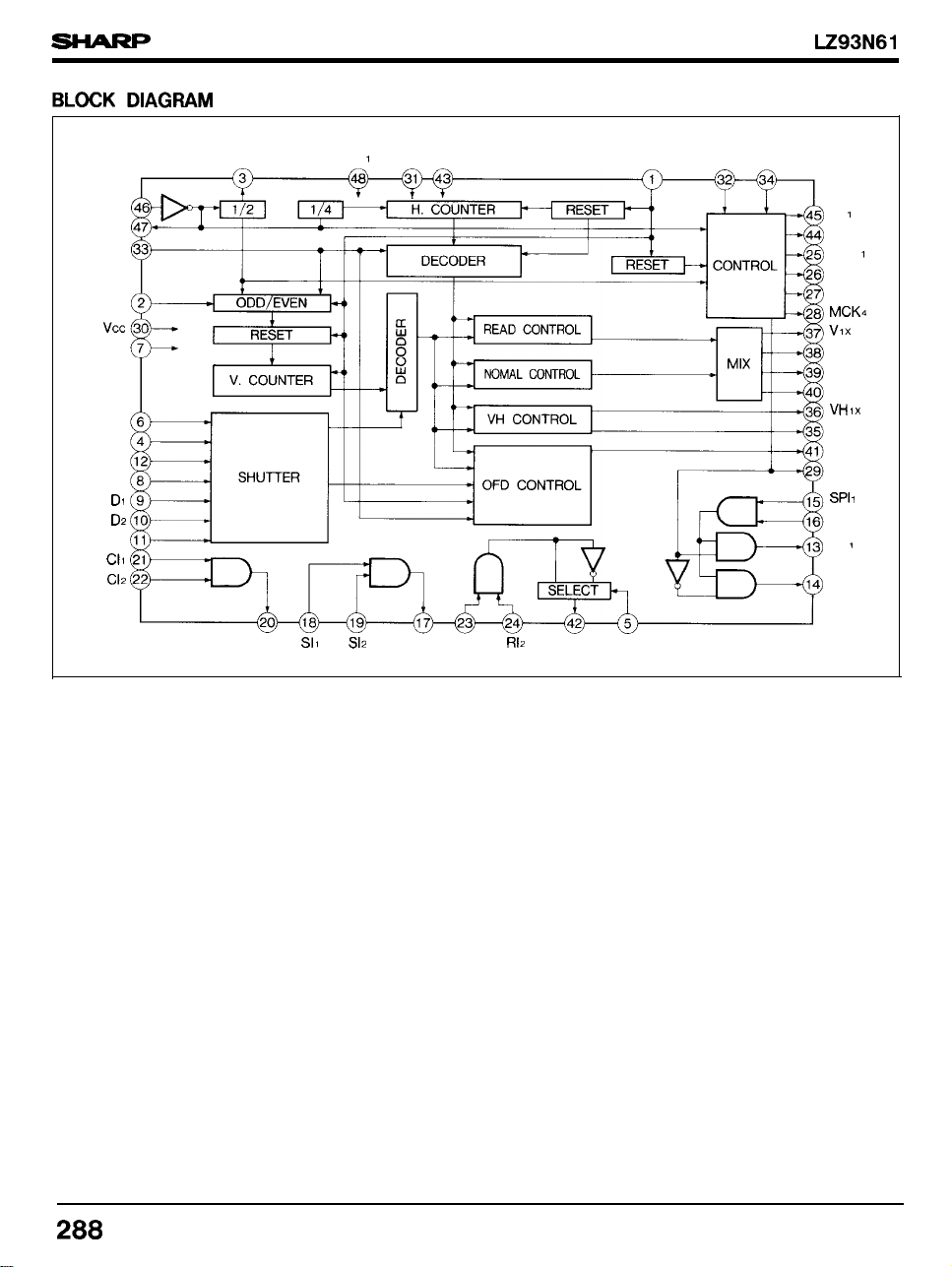
DOUT
TST
GND GND
HDI
SESL SINV
CKI
CKO
TVMD
VDI
GMD
FLMD
PSMD
EXMD
EXST
FH
FH2
MCK
MCK2
MCK3
V2X
V3X
V4X
VH3X
OFDX
Do
FR
FCDS
FS
RI I
FRS
SE
SPI 2
SP
SP2
Page 3
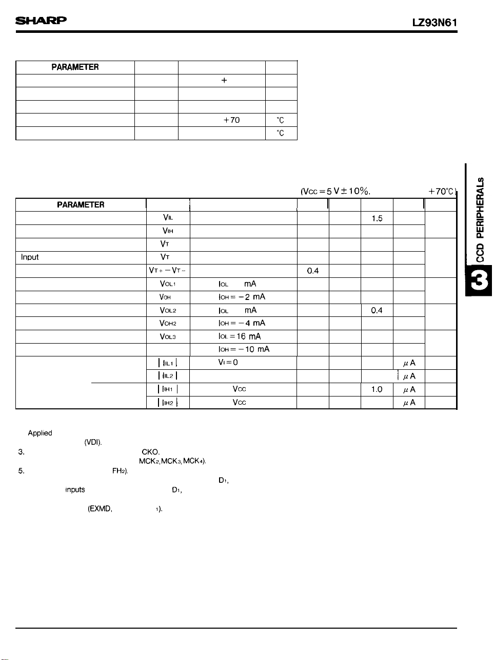
ABSOLUTE MAXIMUM RATINGS
SYMBOL
Supply voltage
Input voltage
Output voltage
Operating temperature
Storage temperature
Vcc
VI
Vo
Topr
Tstg
RATING
– 0.3 to
–0.3 to Vcc + 0.3
– 0.3 to Vcc + 0.3 v
–20 to
–55 to +150
UNIT
v
DC CHARACTERISTICS
Input Low voltage
Input High voltage
Input High threshold voltage
Hysteresis voltage
Output Low voltage
Output High voltage
Output Low voltage
Output High voltage
Output Low voltage
Output High voltage
Input Low current
Input High current
NOTES :
1.
2. Applied to
Applied to
4. Applied to
Applied to
6. Applied to
7. Applied to
8. Applied to
9. Applied to
all inputs except for VDI, CKI.
input
all outputs except for
outputs (FR, MCK I,
outputs (FH 1,
all inputs except for PSMD, FRS, FLMD, Do,
(PSMD, FRS, FLMD, Do,
all inputs except for EXMD, TVMD, TST
inputs
TVMD, TST
SYMBOL
1
v0H3
CONDITIONS MIN.
= 4 mA
mA
=8 mA
mA
mA
mA
v
Vl=o v
VI= Vcc
VI= Vcc
D2, EXST, SESL, SINV
D2, EXST, SESL, StNV).
1.
Ta=–10 to
TYP. I MAX.
3.5 v
2.2
1,0
4.0 v
4.0
4.0
8.0
8.0 60
UNIT
3,8
2.4 v
0.4
0.4
1.0
60
v
v
v
v
v
v
v
NOTE
1
2
3
4
5
6
7
8
9
289
Page 4
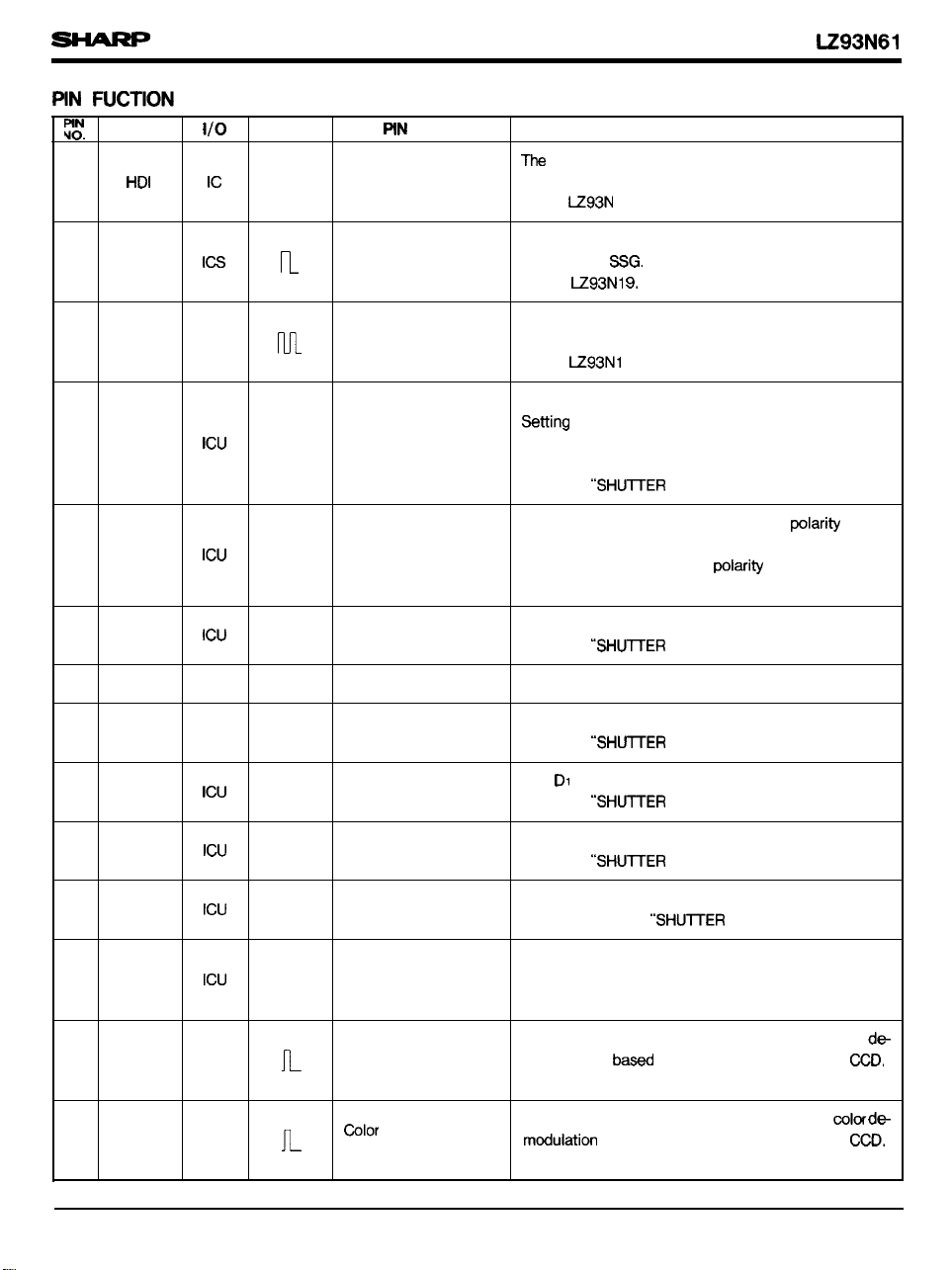
SYMBOL
1
2
VDI
3 DOUT
4 PSMD
FRS
5
o
POLARITY
MM
NAME
Horizontal drive pulse
Vertical drive pulse
Delay-Line clock
Shutter mode select
input
FR control input
FUNCTION
HDI pin is used to input the horizontal reference
signal from SSG. It is connected to the HD (pin 31)
of the
The VDI pin is used to input the vertical reference
signal from
of the
The DOUT pin output 1/2 dividing clock input to
the CKI (pin 46). It is connected to the CLKI (pin 27)
of the
The PSMD pin is used to switch the Shutter Speed
(Refer to
The FRS pin is used to selects the
FR (pin 42).
19.
It is connected to the VD (pin 34)
9.
mode.
High level : Parallel Setting mode
Low level : Serial Setting mode
High level : negative ~larity
Low level : positive polarity
6
FLMD
7
6
9 D
10
11
EXST
12
EXMD
13
14
GND
Do
I
D2
SP1
SP2
— —
Icu
o
o
Flicker-less mode
select
Ground
Shutter speed
—
switching input O
Shutter speed
—
switching input 1
Shutter speed
—
switching input 2
Shutter speed
—
control 1
Shutter speed
—
control 2
Color sampling
pulse 1
pulse 2
The FLMD pin is used to prevent the flicker.
(Refer to “SHU~ER MODE TABLE ”.)
The GND is a ground pin.
The Do pin is used to control the shutter speed.
(Refer to
The
pin is used to control the shutter speed.
(Refer to
The D2 pin is used to control the shutter speed.
(Refer to
The EXST pin used to control the shutter speed 1 H
by 1 H. (Refer to “SHU~ER MODE TABLE ”,)
When the EXMD input pin is Low level, the EXST
(pin 11) is prohibited. (Refer to “SHUTTER MODE
TABLE” .)
The SPI pin output the sampling pulse for color
modulation
It outputs at High level of the SE (pin 29).
The SP2 pin output the sampling pulse for
based upon the output signal of
It outputs at Low level of the SE (pin 29).
MODE TABLE”. )
MODE TABLE ”.)
MODE TABLE ”.)
upon the output signal of
290
Page 5

15
--------
I
PIN NAME
SPI
and SP2 phase
control input 1
The
pin sets the falling edge of
pulses
(pin 13) and SP2 (pin 14).
sampling
16
17
18
19
20
21
22
23
24
25
26
SP12
FS
1
FCDS
c11
C12
RI
MCKI
MCK2
and
control input 2
o
o
o
o
CDS pulse 2
FS phase control input 1
FS phase control input
FCDS pulse 1
FCDS phase control
input 1
FCDS phase control
input 2
FR phase control
input 1
FR phase control
input 2
Clock output 1
Clink output 2
phase
The SP12 pin sets the rising edge of color sampling
pulses SPI (pin 13) and SP2 (pin 14).
The FS pin outputs the pulses for sampling output
signals of
The
pin sets the phase of the FS (pin 17).
The
pin sets the width of the FS (pin 17).
The FCDS pin outputs the pulse to clamp the out-
put signals of
The Cl
pin sets the phase of the FCDS (pin 20).
The
pin sets the width of the FCDS (pin 20).
The RI I pin sets the pahse of the FR (pin 42).
The
pin sets the width of the FR (pin 42).
The MCKI pin outputs 1/2 dividing pulse of
46). It is the same phase with the FH
The MCK2 pin outputs 1/2
46). It is delayad by approximately
respect to FH1 (pin 45).
in phase with
(pin
(pin 45).
(pin
27
28
29
31
MCK3
MCK4
SE
GND
o
o
o
–
–
Clock output 4
Color demodulation
—
Power supply
Ground
–
MCK3 pin outputs 1/2 dividing pulse of
46). It is the same phase with the
The
46). It is delayed by approximately
respect to FH2 (pin 44).
The SE pin outputs the demodulation carrier of output signals of CCD, and input the switching signal
of color sampling pulses
14). It outputs 1/4 dividing pulse of the
(pin 46), and selects the phase in
the SESL (pin 32) and the SINV (pin 34).
The Vcc is a + 5 V power supply pin.
The GND is a ground pin.
pin outputs 1/2 dividing pulse of
in phase
(pin 13) and
(pin
(pin 44).
(pin
(pin
input
with
291
Page 6

SYMBOL
32
SESL
33 TVMD
POLARITY
—
– TV mode input
PIN NAME
FUNCTION
The SESL input pin selects the phase of color demodulation carrier output SE (pin 29).
Low level : synchronized with the rising edge
of FHI (pin 45).
High level : synchronized with the rising edge
of FH2 (pin 44).
The TVMD input pin selects the TV system.
Low level : NTSC system
Hige level : PAL system
34
VH3X
35
36 VH
37
38
39
41
OFDX
42
43
GND –
44
VI x
V2X
V3X
V4X
FR
FH2
—
0
IX
0
o
o
o
o
o
02
–
05
line input
Read out pulse 3
Read out pulse 1
Vertical transfer pulse 1
Vertical transfer pulse 2
Vertical transfer pulse 3
Vertical transfer pulse 4
OFD pulse output
Reset pulse
Ground
Horizontal transfer The FH2 pin outputs the horizontal transfer pulse of
pulse 2 CCD shift register. It is connected to the
The
modulation carrier output SE (pin 29) at 1 H rate.
VH3X is a pulse output pin to transfer the photc-
The
diode charge of CCD to the vertical shift register.
It is connected to the 3BX (pin 11) of the LR366B3N
vertical driver
The VHIX is a pulse output pin to transfer the photcdiode charge of CCD to the vertical
is connected to the 1 BX (pin 8) of the
vertical driver
The V
I x, V2X, V3X and V4X are transfer pulse output
pins for CCD vertical shift register,
The OFDX pin is used to output for controlling OFD
voltage during electronic shutter operation.
The FR pin outputs the reset pulse of CCD. It is
connected to the ~ R through the offset circuit.
The GND is a ground pin.
register.
46
45
FH
I
05
CKI ICK
Horizontal transfer The FHI pin outputs the horizontal transfer pulse of
pulse 1 CCD shift register, It is connected to the
is a reference clock input pin of horizontal
The
and vertical pulses,
Frequency for NTSC
Clock input 1212
Frequency for PAL
: CCD of 542 horizontal pixels.
: CCD of 542 horizontal pixels.
1236
= Horizontal frequency)
Page 7

I47I
SYMBOL
CKO
POLARITY
OCK
I
I
PIN NAME
Clock output
I
FUNCTION
The CKO pin outputs clocks at the reverse of the
CKI (pin 46).
48
TSTI
Input pln (CMOS level).
:
Input pin
:
Input pin
ICD :
Input pin
:
Input pin for oscillation.
ICK :
Output pin for oscillation.
OCK :
Output pin.
0:
Output pin.
02 :
Output pin.
05 :
ICD
(CMOS level with buflt-in pull-up resistor).
(CMOS level with built-in pull-down resistor).
(CMOS level schmitt).
-
Test terminal 1
The TSTI input pin is normally kept
open.
Page 8

SUPPLEMENTARY EXPLANATION
MODE TABLE
INPUT PIN
Ps
FL
MD MD MD MD ST
PIN
4 6 33
H H
H H
I
H H
H H
n.
H
H
H
L
L
L
L
L
L
L
L
L
L
L
L
L
L
L L
L
H
H
H
H
H
H
H
H
H H
H H
H
H
H
L
I
EX EX
‘2“
12
11
10
L L
L L
1 1 1
L L
L L
L
L
L
L
H
L
L
L
L
L
L
L
L
L
L
L
L
L
L
L
L
L
L
H
L
H
1
1
H
H
H H
H H H
I
9 8
L
L
H
H H
L
L
1 1
REGISTER IN
D,
D5
D4
D3 D2
L NORMAL
H
1
I
1
L
L 1/1 000
H
L
1
1 1 1
H H
H H
H H
H
H H
H H
H H
H H
H H
H
H
H
H
L 1/100
L
L 1/120
H
L
L L 1/120
1
L
L
L
L
L
H
L
H H
H
L
H
L
H
H
H
H H
L
SPEED (S]
1 /125
1 /250
1 /500
1/2 000
1/4 000
1/10000
.
1/
1/120
L
NORMAL
H
L
L 1/1 000
H
L
1/125
1 /250
/500
1/2 000
1/4 000
1/10000
1/100
OFDX = H
1/100
1/120
OFDX = H 2
EXST
LZ93N61
NOTE
1
I
I
3
I
NOTES :
1.
2. The data of shutter speed was decided by the control pulse EXST (pin 11), is deleted.
S,
3. The shutter
4. The data of shutter
When power is turned on in Serial mode
= H), the mode is not established until data is input from serial code or
S.
was decided by the control pulse EXST (pin 11), hold as it is
= L) or External Trigger mode
Page 9

SERIAL DATA FORMAT
D I (pin 9)
(pin 10)
Do
D2 D3 D. D,
D7
Do (pin 8)
NOTE :
are latched by the rising edge of pulse D, (pin 9).
By the falling edge of pulse Do (pin 8), the shutter
DESCRIPTION OF EXTERNAL SYNCHRONOUS SHUTTER MODE
1. When EXMD = H, this mode is given priority over other
modes. On applying falling edge of trigger input to
EXST (pin 11), the
reads at the rising edge of HDI
and latches the V period counter value, and controls
final output of the OFDX pulse during this H period.
(The pulse must lasts until HDI goes high.)
2. Once latched, the value of V period counter is retained until the next trigger is input as long as EXMD
= H, even trigger input is for odd (ODD)
even (EVEN)
field, the storage time of another field becomes the
same as the field with trigger input automatically.
NTSC
PAL 19/331 H
HOI
EXST
(PATTERN)
17/279 H 18/280 H 19/281 H 20/282 H 21/2S3 H
n n
b (INVALID)
a
H
C (EVEN
n
speed is decided.
Note that when changing in high speed shutter direction, the internally stored data is used first, This
the delay to control by one field.
[Trigger input disabled range]
To match ODD storage time with EVEN
time, the
pulse start position is set at 20/283 H for NTSC and
22/335 H for PAL. This means that inputting the trigger
at 18/280, 281 H in NTSC mode and 20/332, 333 H in
PAL mode is made disabled.
I-1
H
H
n
H
e
OFDX
(PATTERN)
4th FIELD
,
a c d e
END
000 START EVEN START
Page 10

TIMING
CBLK
VDI
VI
V2X
V3X
V4X
VH3X
OFDX
(EVEN FIELD)
CBLK
HDI
..-.
n@2n4wn4ffiflwn4mn4’2fl
V2X
V3X
V4X
VHIX
VH3X
OFDX
(l St,
3rd
FIELD)
CBLK
HDI
VDI
V2X
V3X
V4X
VHIX
VH3X
OFDX
525 1
n
n
++
465 487
u u u u
nnn
++++
u
11
u u u
623
nnn
n
u u
u
u
u u
VERTICAL PULSE TIMING < NTSC > Shutter speed
1
n
nnnnn nnnnn
n
1
491
n
n
n
----- -----
u uuu u
n
u
263
n
n
nnn
nnnnn
n
u u
n n
u uuu
VERTICAL PULSE TIMING < PAL >
625 1
nnn n n n
n
n n n n
u
u
uuu
uuu
u
n n
11
u u u u u u u
10
n
n
n nnn n
n
n
n
n
nnn
u
u u
u
nnn n
. . ----- ----
II
u
272 283
n
n n
nnn
u
n n
u
u
n
n
u
u
u u
u
10 16 21 23
n
n n
nnn
u
u
u
nnn n
n
n
n n n n
u u u
uuu u u u
nnn
n
u
u u uuu u
u
n
n n nnn n
n n
n nnn n
11 11
21
nnn n
n
59111315
n
n n n n
n
u
I
n n
n
+++++
3579111315
n
n
n
u
n
u u
u u u
n
n
u u
u
u
u u
1/10000 s
n
n n
uuu
n
n
n
uuu
Shutter speed
1/10000
. . .
3
246
n n
u u
u u u
++
n
u
s
n
—
(2nd,
4th
CBLK
HDI
VDI
V2X
V3X u
V4X
VH3X
OFDX
310
n n
n
u u11u u uuu
u
u u u
nnn
n
n n
318 332 336
n
n n n
n n n n
u u u
n
n n
uuu u
u
u uuu u u u u u uuu
n
n
n
n n
n
11
u uuuuu u
n n n
n n
n
nnn
n nnn
u
u
n
n
n
146
n
n
u u
u u u u
I
357
n
u u
n n
n
n
u
Page 11

(ODD FIELD)
VI
V2X
V3X
CHARGE READ TIMING < NTSC >
H
x
98
78
898
19 H
121 2(01
120
118
78
VH3X
OFDX
(EVEN FIELD)
VH3X
OFDX
3rd FIELD)
VHIX
VH3X
OFDX
(2nd, 4th FIELD)
HD
V2X
V3X
V4X
HD
VIX
V2X
V3X
V4X
HD
x
V2X
V3X
332 H
o
I
H
I
II
281 H
2(o) 120
128
CHARGE READ TIMING < PAL >
812 7M
-1
333 H
12WOI
118
128
I
118 322
28
—
—
VH3X
OFDX
Page 12

DOUT
FH
FH2
HORIZONTAL PULSE TIMING
PAL
o
120
169 (193)
.
SE
V2X
V3X
V4X
OFDX
SINV SESL
LL
LH
T
x
58
48 108
6s
98
78
118
128
140
15s
 Loading...