

Page 1

LZ95B25
Subcarrier Generator
for CCD
DESCRIPTION
The U95B25 is a CMOS subcarrier signal generator LSI which provides
color video camera, in
combination
pulses for
LSI (LZ95D52/M)
FEATURES
.
systems
. Included phase comparator circuit
● Single + 5 V power supply
● Package : 18-pin MFP(MFPO1 8-P)
RI
between
PAL and
Vcc GND CPI SCHD RPI CFMI TST, CPCH EOO
PIN CONNECTIONS
18-PIN
0
2
4FSI 3
4FS0 4 15 SCHD
I 5 14 RPI
TST
6 13 CFMI
SC2
7
TST2 8 11 CPCH
GND 9 10 EOO
TOP VIEW
18
17 GNO
16 CPI
12 TST3
TVM2 4FSI 4FS0
TVM
‘In the abwnce of confimtion by device sw!fication sheets SHARP takes no rewnslb!l(v fci any defects
SHARP
in
ws,on of
device m.lhcation
SC2 TST2 GNO
in
anv SHARPs device”
any of WARPs devices, shorn
cablcgs,
299
Page 2
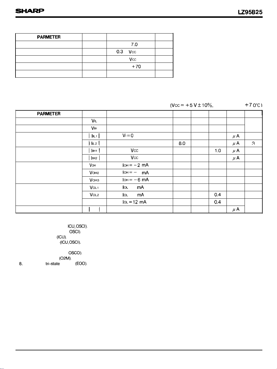
ABSOLUTE MAXIMUM RATINGS
SYMBOL
Supply voltage
Input voltage
Output voltage Vo
Operating temperature
Storage temperature
Vcc
VI
Topr
Tstg
RATING
–0.3 to
–
to
+ 0.3
–
0.3
to
+ 0.3
–20 to
–55 to +150
UNIT
v
v
v
‘c
“c
DC CHARACTERISTICS
Input Low voltage
Input High voltage
Input Low current
Input High current
Output High voltage
Output Low voltage
Leak output current
NOTES :
1. Applied to inputs (IC,
2. Applied to inputs (lCD,
3. Applied to input
4. Applied to inputs
5. Applied to input (lCD).
6. Applied to outputs (O,
7. Applied to output
Applied to
output
SYMBOL CONDITIONS MIN. TYP.
3.5
v0L3
Ioz
1
v
Vl=o v
VI=
VI=
= 4
= 2
High-Z
8.0 60
I
4.0 v
4.0 v
4,0 v
Ta=–10 to
MAX. UNIT NOTE
1.5
1.0 ,uA
0.4
1.0
v
v
v
v 7
v
1
2
4
5
6
7
8
6
8
300
Page 3

2
3
SYMBOL
_..
TVM
TVM2
4FSI
I POLARITY I
Icu
—
—
PIN NAME
TV mode 1
TV mode 2
FUNCTION
These input pins to select TV standards.
An input pin for the signal 4 times the color sub-
carrier frequency.
: 14.31818 MHz
At PAL mode
At SECAM mode : 17.625 MHz
: 17.734475 MHz
The output is the inverse 4FSI (pin 4).
A test pin, Set open or to L level in the Normal
mode,
An output pin fw color
the signals is 1/4 the 4FSI (pin 3). The signal is
reset by color frame pulse
An output pin for color
of
80 degree in NTSC
of SC2 is
and 270 degree when LSW is H level. The SC
same as the phase of SC I in SECAM mode.
A test pin. Set open or to L level in the Normal
mode.
A grounding pin.
Phase comparator output for input signals RPI (pin
14) and
is Low level. When
level. When phases are equal, the terminal impad-
ance is High.
edge of
The CPCH input pin switches the polarity of RPI
(pin
level, phase comparator comparates falling edge
of
(pin 16). When
is delayed, output is High
comparator comparates rising
When CPCH is L level,
The frequency of
When the phase
is
is L level
is
is advanced, output
comparator
—
—
—
—
—
Clock output
Test pin 1
output 1
Test pin 2
Ground
Phase comparator
output
Polarity select input comparates rising edge of RPI. When CPCH is H
4FS0
4
TSTI
5
6
SC2
7
TST2
8
GND
9
10
CPCH
11
Osco
02M
02M
ICD
—
TO
12
TST3
13
–
–
Test pin 3
Color frame input
A test pin. Set open or to L level in the Normal
mode.
An input pin for color frame signal; Connect to
CFMO
301
Page 4

SYMBOL
14
15 SCHD
RPI
ICD
o
POLARITY
—
–
PIN NAME
Horizontal comparison
input
FUNCTION
An input pin for the reference horizontal signal to
the phase comparator. Connect to HD (SSG-LSI),
when comparator is used. The polarity of RPI selects with CPCH (pin 11),
A horizontal synchronous pulse obtained by dividing
4FSI (pin 3).
At NTSC mode
At PAL mode
At SECAM mode : dividing into 1/1 128
: dividing into 1/910
: dividing into 1/1 135 4FSI
ordinarily and dividing into
rizon tal period within the V
blanking.
16
17 GND
18
Icu
ICD
o
02M : Output pin.
TO
OSCI : Input pin for oscillation.
OSCO : Output pin for oscillation.
CPI
—
–
:
Input pin (CMOS level with built-in pull-up resistor).
: Input pin (CMOS level with built-in pull-up resistor).
:
Output pin,
: Output
–
—
.
output).
Horizontal comparison
input
Ground
Power supply Supply +5 V power.
An input pin for comparison horizontal signal to the
phase comparator. Connect to SCHD (pin 15) when
comparator is used,
A grounding pin.
302
Page 5

TIMING DIAGRAM
4FSI
4FSI
LSW
PULSE TIMING < NTSC >
SC2 :
advanced
PULSE TIMING < PAL
4FSI
: 90” advanced
PULSE TIMING <
: same phaw
delayad
SC2 :
>
1
1
303
 Loading...