

Page 1
Synchronous Signal Generator for CCD
DESCRIPTION
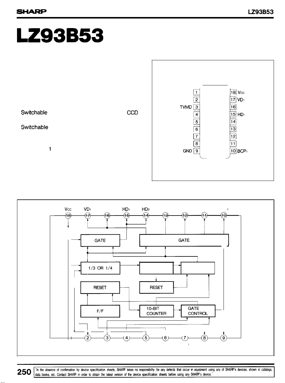
The LZ93B53 is a CMOS synchronous signal
generator LSI which provides B/W TV synchro-
nous pulses and video signal processing pulses,
in combination with the timing signal generator
LSI (LZ93N61, LZ95F50, or LZ93F33).
FEATURES
.
and 320000 pixels B/W CCD
.
● Single + 5 V power supply
. External synchronization is possible
. Package :
between 270000 pixels B/W
8-pin MFP(MFPOI 8-P)
BLOCK DIAGRAM
VD2 HDI
PIN CONNECTIONS
18-PIN MFP
CBLK
CLKI 1
CLKO 2
CPMD 4
CKMD 5
TSTI 7
TST2 8
HBLK CSYN
0
3
VRI 6
TOP VIEW
17
16 VD2
15
14 HD2
13 CBLK
12 HBLK
11 CSYN
10
BCP
CLKI
7-BIT
COUNTER
CLKO TVMD CPMD CKMD
I
VRI TST
GATE
CONTROL
TST2
GND
Page 2
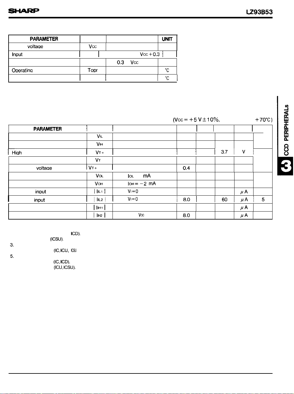
ABSOLUTE MAXIMUM RATINGS
SYMBOL
Power
voltage
Output voltage
VI
Vo
temperature
Storage temperature
Tstg
DC CHARACTERISTICS
SYMBOL
Low level input voltage
High level input voltage
level threshold voltage
Low level threshold voltage
Hysteresis
Low level output voltage
High level output voltage
Low level
LOW level
High level input current
High level input current
current
current
–VT-
RATING
– 0.3 to 7.0
-0.3 to
–
to
–20 to +70 ‘c
–55 to +150
CONDITIONS
Schmitt buffer
Schmitt buffer
Schmitt buffer
VI= Vcc
VI= Vm
=4
v
+ 0.3
v
v
v
v
MIN.
3.5
1,0
4.0
TYP.
Ta=–20 to
MAX.
1,5
0.4
1.0
1.0
UNIT
v
v
v
v
v
v
NOTE
1
2
3
4
6
7
NOTES :
1.
Applied to inputs (IC, ICU,
2. Applied to input
Applied to all outputs (0).
4. Applied to inputs
Applied to input (lCD).
6. Applied to inputs
7. Applied to inputs
).
251
Page 3

PIN FUNCTION
10.
1
CLKO
2
3
CPMD
4
o
ICD
—
—
Main clock
Clock out
TV mode select
Clamp pulse mode
select
This is a pin to input the clock which is used as
the reference of the horizontal and vertical pulses.
This pin should be connected to DO on the timing
The frequency varies depending on CKMD (pin
5) as follows.
●
system
270000 pixels fck : 9.534964 MHz(606 fH)
360000 pixels fck : 12.713285
system
.
320000 pixels fck : 9,656250 MHz(6I 8 fH)
pixels fck : 12.875000 MHz(824 fH)
420
This is an inverted output pin for CLKI (pin 1).
This is a pin to select TV systems.
● Low level
● High level :
system
system
This is a pin to control stop and continuance of
BCPI (pin 10) within the vertical blanking period.
● High level : BCPI outputs continuous pulses.
● Low level : BCP I stops outputting composite
pulses while there is no effective
pixel within the V blanking period.
This is an input pin to switch the frequency devision
in accordance with the area sensor as follows.
–
CKMD
5
Clock mode select
Frequency division
output
CKMD
Number of pixels
1/3
High
270000
1/4
Low
360000
This is an input pin for the external V reset pulse
which is used to apply vertical synchronization to
the counter (2 fck counter) on the synchronization.
This resetting takes priority over the internal resetting. Since the rise of input at
is taken at the
horizontal synchronous frequency (2 fH) which is two
times as high as the internal frequency, when the
VRI
6
u
Vertical reset
vertical pulses which were separated in terms of
frequency from the composite synchronous signal
from other equipment are used, the fall must have
a phase difference of less than 1/2
compared
with the start timing of the vertical synchronous
signal. When the
synchronization is obtained,
the High level should be selected. The input is designed as a
Test
7
–
1
This is an input pin for tests, Typically, this pin
should be open or at the Low level.
trigger buffer.
Page 4

9
10
11
12
13
14
15
16
17
SYMBOL
GND
BCP
CSYN
HBLK
CBLK
HD2
HDI
VD2
VDI
Vcc
PIN NAME
Test
Ground
o
I
o
o
o
o
o
o
n
0
Optical block clamp
pulse
Composite synchronous
signal
Horizontal blanking
pulse
Composite blanking
pulse
Horizontal drive pulse 2
Horizontal drive pulse
Vertical drive pulse 2
Vertical drive pulse
Power supply
2
This is an input pin for tests. Typically, this pin
should be open or at the Low level.
This is a grounding pin.
This pin output pulse which is used to clamp opti-
cal black on each line of the sensor output, Typically, these are horizontal synchronization continuous
pulses. However,
level allows the composite output which becomes
the Low level while there is no effective pixel within
the vertical blanking period.
This pin outputs
synchronous signals.
●
system
.
This pin outputs a pulse to stop
fer pulses which drive the horizontal register in the
area sensor.
This pin outputs pulses which are used for video
blanking in the encoder.
system : 11.01 ps, V20 H is cleared.
.
. CCIR system :
This pin outputs pulses which are synchronous with
the start of each line and used as the H reference
of the timing
This pin outputs pulses which are synchronous with
the start of each line and used as the H reference
of external equipment.
This pin outputs pulses which are obtained at the
start of each field and used as the V reference of
the timing
This pin outputs pulses which are obtained at the
start of each field and used as the V reference of
external equipment.
supply +5 V power
FUNCTION
CPMD (pin 4) to the Low
and CCIR standard composite
: Compatible with RS-170
horizontal trans-
V25 H is cleared.
: lnDut Din (CMOS level).
ICU : Input pin (CMOS level with pull-up resistor).
ICD : Input pin (CMOS level with pull-down resistor).
ICSU :
o
: Output pin
input pin (CMOS level with pull-uP resistor)
Page 5

TIMING DIAGRAM
(ODD FIELD)
VERTICAL TIMING < EIA >
(EVEN FIELD)
3rd FIELD)
CBLK
CSYN
HBLK
CBLK
CSYN
BCPI
HBLK
CBLK
CSYN
HBLK
523524525 1
HD
VD
n
u
u
n
n
u
260261 262
HD
VD
n
n
u
u
n n n n n n
u
u
234567891011 12131415161718192021 22
n
I
u
n
u
n n n
u
u u
u u
u
uuu u u u
u
u
u
u u u
= L
265266267269269270271 272273274275276277278 279280281 282283284
I
n Iu
u
uuu u
nnn
u
u
n
u u u
u
u
u
CPMD=L
VERTICAL TIMING <
622623624625 1 2 3 4 5 6 7 8 9 10 11 12 13 14 15 16
HD
VD
n n n
n
n
CPMD=L
n
n n n
n
n
u
n
n n
n n n
u u u u
u
u u
u uuu
u
n
u u
u
u u u u
>
u u
u
n
u u
n
n
n
u
u
u
u
n
n
u
u u u
n
n
u
u
u
n
u
u
n n n
u
u
u u
n n
u
u
n n
u
21 22 23 24
n n
n
u
u u
nnn
u
u
u
u
u
n
u
u
(2nd, 4th FIELD)
CSYN
BCPI
HBLK
310311 312313314315316317318 319
HD
u
u u
u
= L
11uu u u
321 322323324325326327328 329
u u
u
u u u
L1
u u
Page 6

HD
CBLK
CSYN
(EQ)
(SAW)
BCPI
–3.15
HORIZONTAL TIMING < EIA >
Unit :
1.57
1,57
1.57
072 2,05
HBLK
1’
NOTES :
Applied to the CCD of 542 horizontal pixels (CKMD = H) : A= 3.88, B = 2.94, C
.
● Applied to the CCD of 726 horizontal pixels
HORIZONTAL TIMING <
HD
CBLK
1.55 6,21
CSYN
155
(EQ)
–3.1
(SAW)
078 2.02
HBLK
= L) : A=3.93, B =2.91, C =8.57
>
=
8.60
Unit : ~s
NOTES :
● Applied to the
● Applied to the CCD of 726 horizontal pixels (CKMD = L) : A
of 542 horizontal pixels
= H) : A =3.83, B =2.90, C= 9.73
B =2.87,
 Loading...