

Page 1
LZ93BE0
Timing Pulse Generator
DESCRIPTION
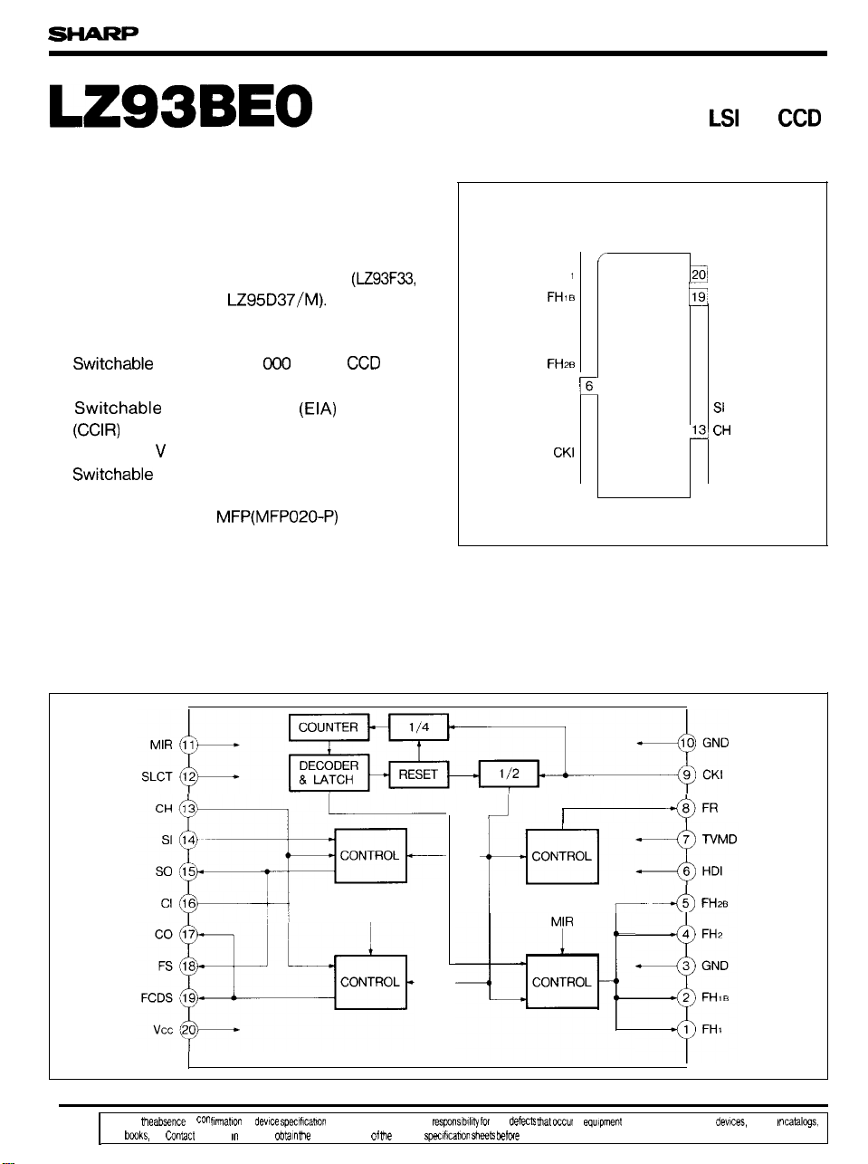
The LZ93BE0 is a CMOS timing generator LSI
which provides horizontal transfer pulse, reset
pulse, and sample-hold pulse used for separate
camera, in combination with single-chip driver
LSI (LZ95G55, LZ95G41 ) and timing LSI
LZ93F50, LZ93N61 or LZ95D37/M).
PIN CONNECTIONS
20-PIN MFP
FEATURES
●
320000 pixels CCD
●
●
Single +5
●
●
Suitable for separate camera
●
Package : 20-pin
☛
Designed for A-type and B-type CCD area sensors :
A-type CCD area sensor : LZ2314J, LZ2324J, LZ231 32, LZ23232
B-type CCD area sensor : LZ2414J, LZ2424J, LZ2313H5,
between 270
pixels
and PAL
systems
power supply
between normal and mirror-image
LZ2323H5, LZ2413, LZ2423
and
FH
GND
FH2
HDI
TVMD
GND
FR
for
TOP VIEW
1
=
o
2
3
4
5
7
8
9
10
Vcc
FCDS
18 FS
17
co
16 cl
15 so
14
12 SLCT
11 MIR
BLOCK DIAGRAM
“in
256
data
of
SHARP
by
order to obkln he latest version device
sheets, SHARP takes no respnslb(l[v
any defecs hat
using any SHARPs device’
in
using any of SHARPs
shown
cahlcgs,
Page 2
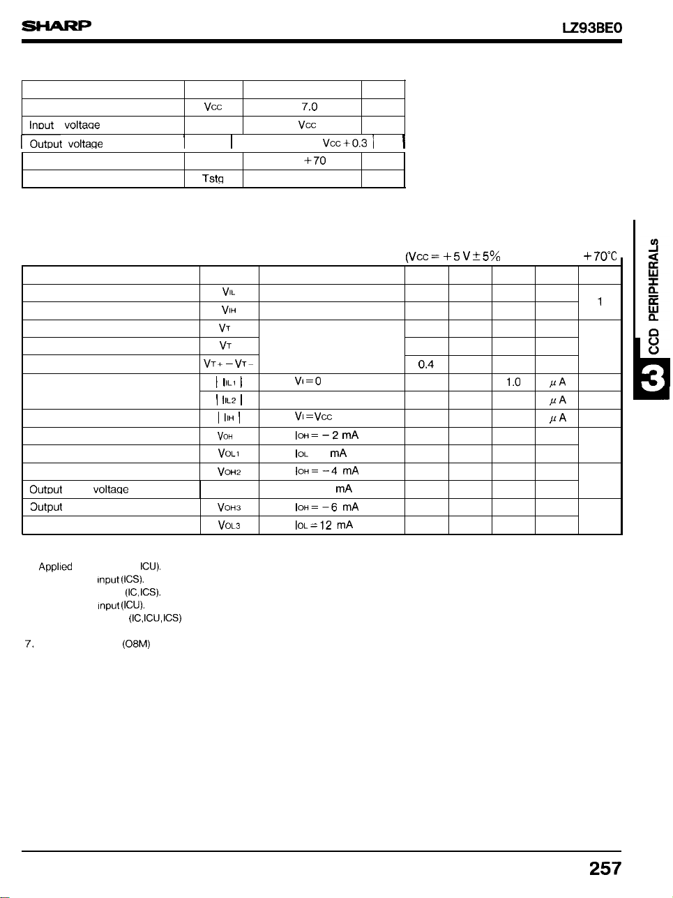
ABSOLUTE MAXIMUM RATINGS
PARAMETER SYMBOL RATING
Supply voltage
voltaae
Operation temperature
Storaae temperature
VI
Vo
Topr
– 0.3 to
–0,3 to
+ 0.3
-0.3 to VCC+O.3
–20 to
–55 to +150
UNIT
v
v
v
‘c
“c
DC CHARACTERISTICS
PRAMETER
Input Low voltage
Input High voltage
Input High threshold voltage
Input Low threshold voltage
Hysteresis voltage
Input Low current
Input High current
Output High voltage
Output Low voltage
Output High voltage
LOW voltaae
High voltage
Output Low voltage
NOTES :
1.
2. Applied to
3. Applied to inputs
4. Applied to
5. Applied to inputs
6. Applied to output (0)
8 Applied to output (012M)
to inputs (IC,
Applied to output (08M)
SYMBOL
IIH
1
v0L2
Ta=–20 to
CONDITIONS MIN.
TYP.
MAX.
1.5 v
UNIT
3.5 v
2.2 3.8 v
Schmitt Buffer 1.0 2.4 v
v
Vl=o v
= 4
IOL = 8
8.0 60
1,0
4.0 v
0.4
4.0 v
0.4
4.0 v
0.4 v
NOTE
2
4
5
v
v
6
7
8
Page 3
1
2
3
4
5
6
7
8
9
10
11
12
SYMBOL
FH
I
GND
FH2
HDI
TVMD
FR
GND
SLCT
012M
08M
–
012M
08M
08M
–
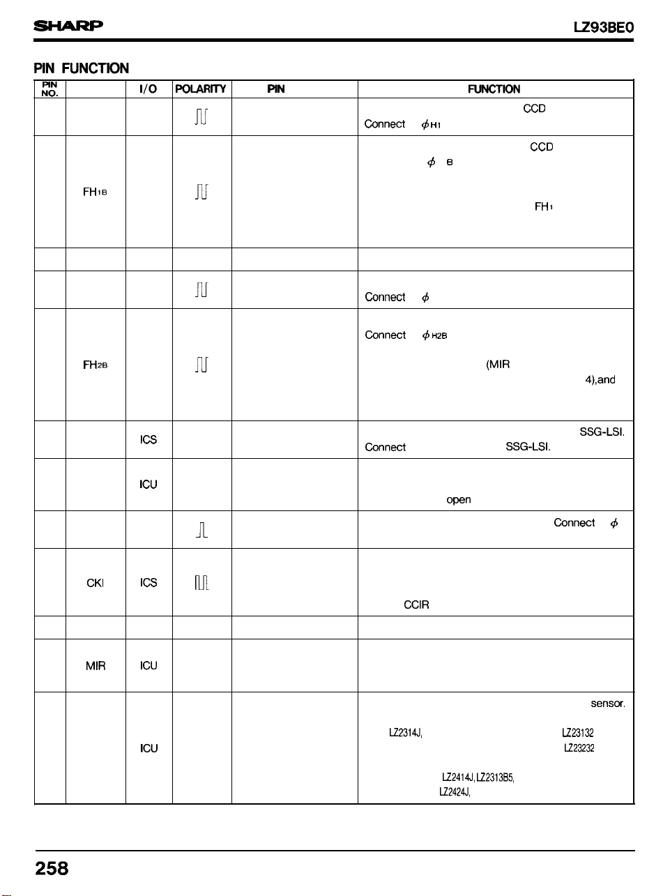
Horizontal transfer
pulse 1
Horizontal transfer
pulse 1 B
Ground
–
Horizontal transfer
pulse 2
Horizontal transfer
pulse 2B
Horizontal reference
–
pulse
TV mode select
–
Reset pulse
Clock input
–
Ground
—
Mirror mode select
—
CCD type select
NAME
A horizontal transfer pulse for
to 4
of CCD area sensor.
A horizontal transfer pulse for
Connect to
of CCD area sensor. If the CCD
area sensor.
area sensor,
area sensor which corresponds to Mirror mode is
driven at Normal mode (MIR = L), its drive-pulse is
the same phase as the pulse of
(pin 1), and it
is the same phase as the pulse of FH2 (pin 4) at
Mirror mode (MIR = H).
A grounding pin.
A horizontal transfer pulse for CCD area sensor.
A horizontal transfer pulse for CCD area sensor.
to 4
of CCD area sensor. If the CCD
area sensor which corresponds to Mirror mode is
driven at Normal mode
the same phase as the pulse of FH2 (pin
is the same phase as the pulse of FH
= L), its drive-pulse is
it
I (pin 1 ) at
Mirror mode (MIR = H).
Put in a horizontal reference pulse from
to HD terminal of
An input-pin to select TV standards,
L level : NTSC mode
H level or
: PAL mode
A reset pulse for CCD area sensor, bnnect to ~ R
of CCD area sensor through the DC offset circuit.
An input pin for reference clock.
The frequencies are as follows :
At EIA mode : 19.06993 MHz (1212 fH)
mode : 19.31250 MHz (1 236 fH)
At
A grounding pin.
An input pin to select Mirror mode or Normal mode.
L level : Normal Drive mode
H level or open : Mirror Drive mode
An input pin to select the type of CCD area
L level (A type)
LZ2314Z, LZ23t42, LZ2313A9,
LZ2324J, LZ2324Z, LZ23242, LZ2323A9,
H level or open (B type)
LZ2314BK,
LZ2324BK,
LZ2313H5, LZ2413
LZ2323B5, LZ2323H5, LZ2423
Page 4

SYMBOL
13
14
15
18
17
18
so o
cl Ic
co o
FS
19 FCDS
Vcc
PIN NAME
FUNCTION
An input pin to select the phase of FCDS (pin 19)
Phase control terminal
—
for FCDS and FS
pulse and FS (pin 18) pulse.
L level : adjustable
H level or open : fixed
Phase-adjust input
for FS
Phase-adjust output
for FS
—
Phase-adjust input
for FCDS
Phase-adjust output
for FCDS
An input pin to control the phase of FS (pin 18).
SO (pin
pulse put in this terminal after make it
delay with resistor and capacitor.
An output pin to control the phase of FS (pin 18).
The output pulse put in
(pin 14) after make it
delay with resistor and capacitor.
An input pin to control the phase of FCDS (pin 19).
(pin 17) pulse put in this terminal after make it
delay with resistor and capacitor.
An output pin to control the phase of FCDS (pin 19).
The output pulse put in Cl (pin 16) after make it
delay with resistor and capacitor.
A pulse to sample-hold the signal from CCD area
o
Sample-hold pulse
output
sensor. The phase of FS is fixed if CH (pin 13)
equals H level and it can be adjustable if CH (pin
13) equals L level.
A pulse to clamp the feed-through level form CCD
o
n
–
CDS pulse output
—
Power supply Supply +5 V power.
area sensor. The phase of FCDS is fixed if CH (pin
13) equals H level and it can be adjustable if CH
equals L level.
(pin
: Input pin (CMOS level input)
: Input pin (CMOS level input with pull-up resistor)
: Input pin (CMOS
O, 08M, 012M : Output pin
NOTE :
the input pin, the rising edge of HDI (pin 6) is
At
input )
20 ns shorter than that of CKI (pin 9).
Page 5

TIMING DIAGRAM
HDI
CBLK
CKI
FH
FCDS
HDI
CBLK
CKI
FH
FH2
FR
FCDS
FR
FS
1212,0
114 120
1212,0 8
NTSC(EIA) < A-TYPE, NORMAL MODE >
49
166
XX X X1212345678
210
1 clock = 52.4 ns
114
< A-TYPE, MIRROR MODE >
clock = 52.4 ns
1
114
CBLK
FH
FH2
FCDS
CBLK
CKI
FH
FCDS
FR
FS
FR
FS
OBIXXX XXX
116 120
n
210
Page 6

HDI
CBLK
CKI
FH 1
FH2
FH2B
FCDS
CBLK
FH
FH2
FCDS
FR
1
NTSC(EIA) < B-TYPE, NORMAL MODE >
163
47
210
1212,0
I
FS
120
14
FR
FS
clock= 52.4 ns
—
HDI
CBLK
CKI
FH
FH2
FCDS
HDI
CBLK
CKI
FH
FH2
FCDS
FS
114 120
FS
1212,0 3
OBIXX X X
XX X X XOB28
< B-TYPE, MIRROR MODE >
0B20
OB1O
OBI 512 510 500 498 496 494 492
1 clock
210
,
ns
111 114
x
261
Page 7

HDI
CBLK
FH
FH2B
FR
FCDS
HDI
CBLK
FH
FH2
B
FS
114 120
I
1236,0
0B4
OB1O
< A-TYPE, NORMAL MODE >
48
OB20
0B28
192
1 clock = 51.8 ns
114
234
m
J
u
FH2B
FR
FCDS
HDI
CBLK
FH
FH2
FH2B
FR
FCDS
CBLK
CKI
FH
FH
FR
FCDS
FS
OBIXXXXXX
FS
114
I
IB
FS
3
20 140
I
u
XX X
< A-TYPE, MIRROR MODE >
m
v
OB20
OB1O
XXXX1212345878 14
1
OB1 512 510
nnLILrLJuLILIL
506 504 502
clock
r
ns
114
234
Page 8

HDI
CBLK
FH
< B-TYPE, NORMAL MODE > 1 clock =51,8 ns
7236,0 47 114
FH2B
FR
FCDS
FS
HDI
CBLK
CKI
FH
FH2
FR
FCDS
FS
HDI
CBLK
CKI
FH
OB4
114 120
M
X X X
OB1O
Ln
234
XXXXXX121234567 8
12 14
< B-TYPE, MIRROR MODE > 1 clock=51.8 ns
3
FCDS
FS
114 120 135 234
CBLK
FH
FCDS
FR
FS
OB1O
OBI 512 510 504
L
500
Page 9

Timing Pulse Generator LSI for CCD
264
DESCRIPTION
The LZ93F33 is a CMOS timing generator LSI
which provides timing pulses used to drive a
area sensor, in combination with the SSG
LSI (LZ93N19 or LZ93B53).
FEATURES
●
320000 pixels CCD
●
●
Built-in EE (Electronic Exposure) control
●
Flicker-less function
●
Switchable between normal and mirror image
●
Single +5 V power supply
●
Package : 48-pin QFP(QFP048-P-101 O)
VDI
between 270000 pixels CCD and
systems
TO GND
and PAL
GND
PIN CONNECTIONS
48-PIN QFP
37 24 MCDI
OFDX
39
FR
40
FH2
42
GND 43
FH
FHIB
45
CKI 46
CKO
47
TEST 48
GND Vcc TEST
0
TSTO
TOP VIEW
23
MFS2
22
21
FS
20
FCDS
19
INSL
18
TO
17
SE
16
SINV
15
SESL
14
SP2
13 SP1
TVMD
ACL
TOSL
DO
CKI
CKO
EEST
EEUD
EENR
EEMD
FLMD
“In be abwnce of
data
Contact SHARP
by
sw[flcahon aheek, SHARP
uder to
wmlon of the
UP/DOWN
CONTROL
SHUTTER
SPEED
CONTROL
no rewnmblllv fci any
shwts
in
using any SHARPs device”
using any of WARPs
VH3X
OBCP
SINV
SESL
FH2
FR
FS
FCDS
SE
SP2
MFSI
MFS2
MFR
MFR2
INS’
OFDX
ca~lws,
 Loading...