

Page 1
LZ93N19
Synchronous Signal Generator for CCD
DESCRIPTION
The LZ93N19 is a CMOS synchronous signal
generator LSI which provides TV synchronous
pulses and video signal processing pulses, in
combination with the timing signal generator LSI
(LZ93N61, LZ93F50, LZ93F33 or LZ95D37/M).
FEATURES
●
320000 pixels CCD
●
●
Single +5
●
External synchronization is possible
●
Package : 44-pin QFP(QFP044-P-101 O)
between 270000 pixels
systems
power supply
and
and PAL
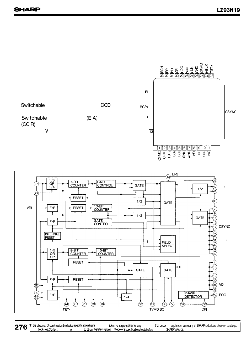
BLOCK DIAGRAM
CLKI
CKMD
CFMI
4FSC
Vcc
GND
GND
PIN CONNECTIONS
44-PIN QFP
c1
VD
34 22
35
CPBL
36 20 FRP
BCPI 37
PBLK
39
HG
40
HG2
41
WBLK 42
4FSC
TST I44
0
m
TOP VIEW
CKMD
21
TST2
19
FRP2
18
TST5
17
16
CBLK
ENCP
15
14
LSW
13
LRST
12
TVMD
/
CPMD
HG
HG2
CPBL
WHD
BF
ENCP
CBLK
HBLK
HD
BCP
BCP2
PBLK
WBLK
CFMO
BFBL
LSW
FRP2
FRP
FI
tie
data
SC2
In
RPI
n
SCHD
swficafm
WARP
waler
WARP
be
of
&v!ce
defects
using any WARPS devce,’
Page 2
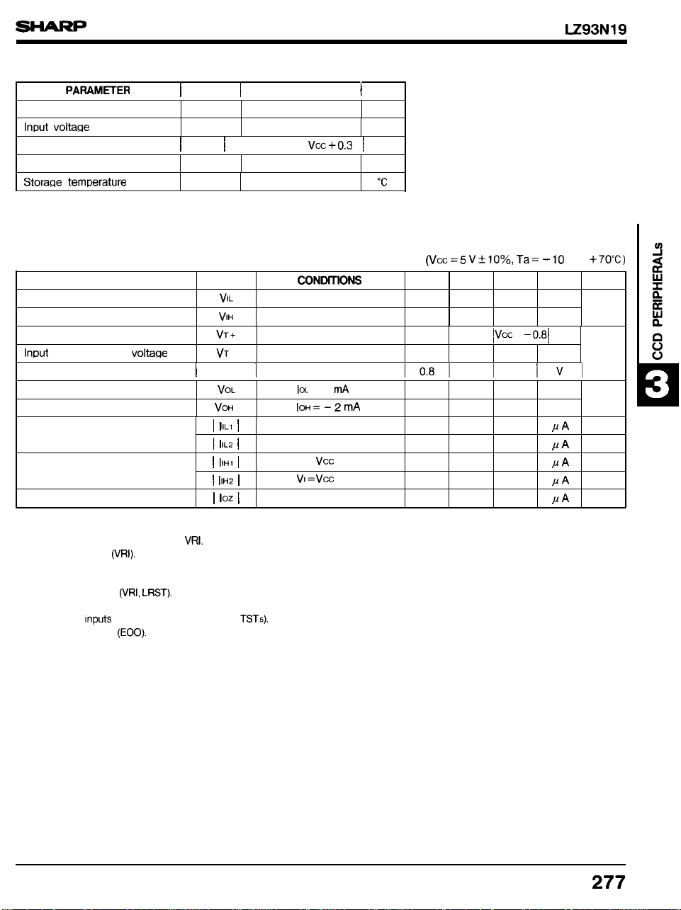
ABSOLUTE MAXIMUM RATINGS
SYMBOL
Supply voltage
voltaqe
Output voltage
Operating temperature
Vcc
VI
Vo
Topr
Tstr
RATING
–
0.3
to
–
0,3
to Vcc +
-0.3 to
–20 to +70
–55 to +150 ‘c
7.0
0.3 v
UNIT
v
v
“c
DC
CHARACTERISTICS
PARAMETER
Input Low voltage
Input High voltage
Input High threshold voltage
Low threshold voltaqe VT -
Hysteresis voltage
Output Low voltage
Output High voltage
Input Low current
Input High current
Leak Output current
NOTES :
1. Applied to
2. Applied to
3. Applied to
4. Applied to
5. Applied to
6. Applied to
7. Applied to
8. Applied to
all inputs except for
input
all outputs.
all inputs except for VRI, LRST.
Inputs
all inputs except for TST 1, TST2, TST3
output
SYMBOL
VT+-VT-
Ioz
MIN. TYP. MAX.
3.5
0.9
=4
Z
4.0
Vl=o v
Vl=o v
VI=
High-Z 1.0
TST4, TST5
8.0 60
8.0
1.5
0.4
1,0
1,0
60
to +70”C)
UNIT NOTE
v
v
V
v
v
v
1
2
3
4
5
6
7
8
Page 3
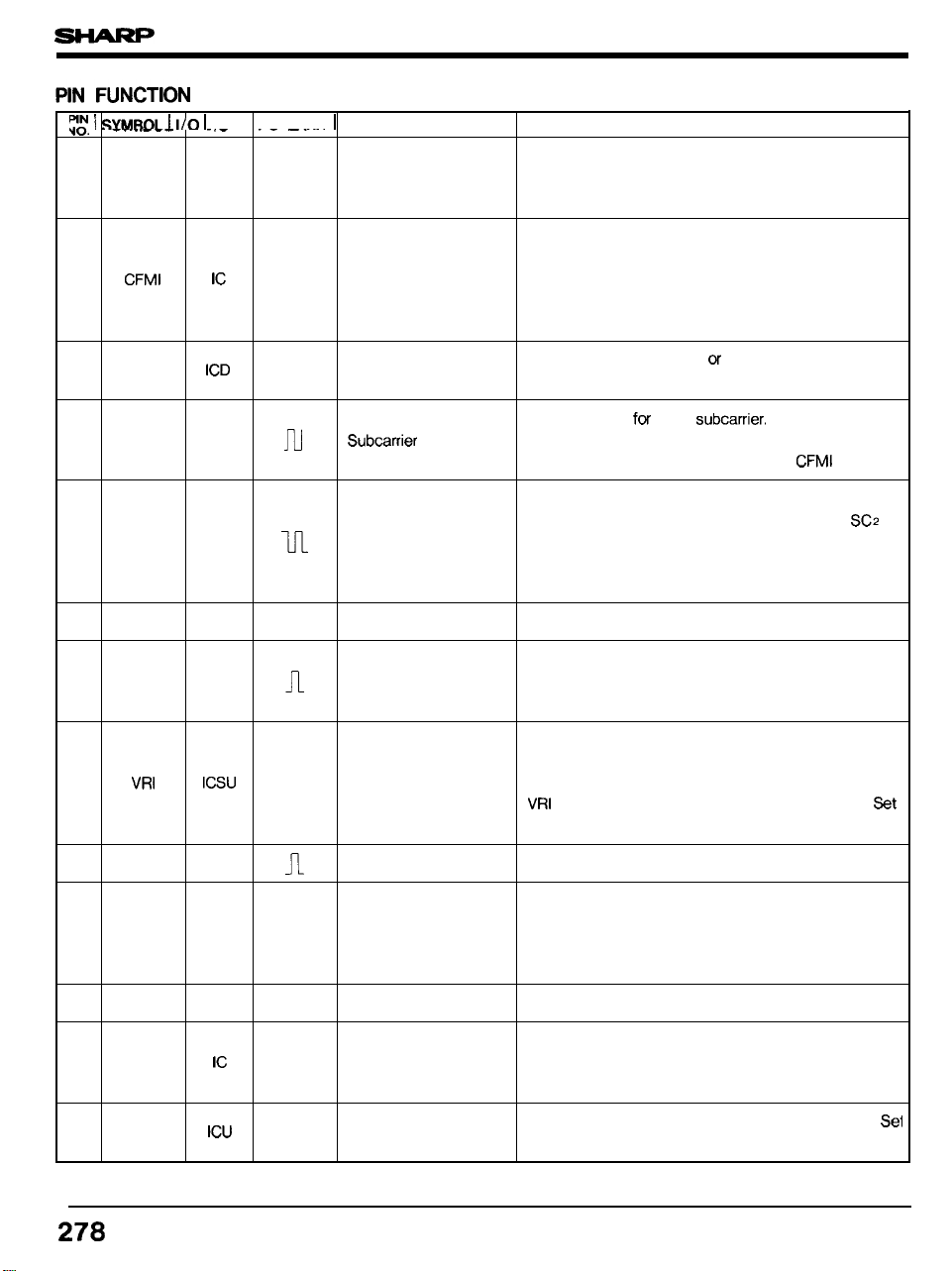
LZ93N19
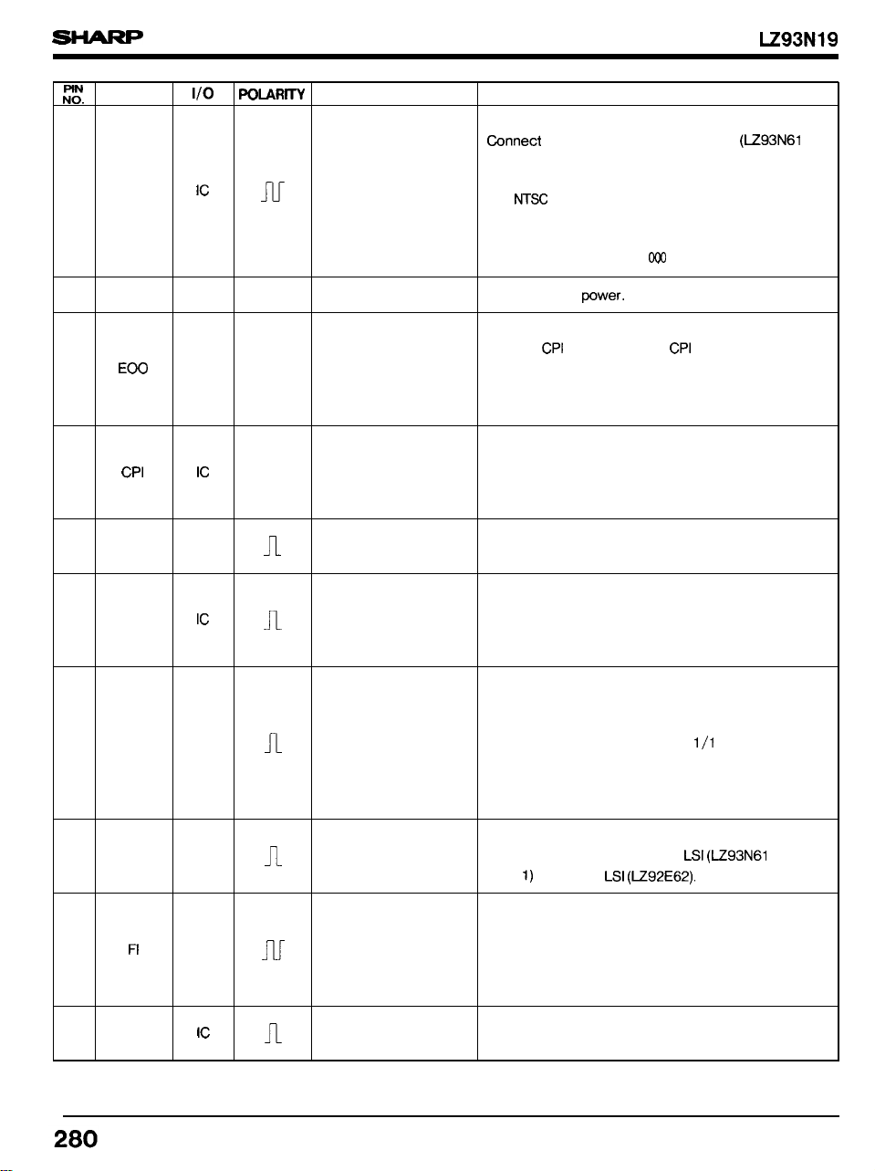
1
CFMO
2
TST3
3
Scl
4
5
SC2
GND
6
7 WHD
1/0
POLARITY
o
o
o
— —
o
PIN NAME
bier frame output fields in NTSC rode, recurs at every 8 fields in PAL
n
Color frame input
n
—
Test terminal 3
Subcarrier output 2 90 degree in NTSC mode in PAL mode, the phase
Grouding
Wide Horizontal
drive output
I
A pulse to control color frame; occurs at every 4
mode.
An input pin for color frame signal. Connect to
CFMO (pin 1) in Internal Synchronous mode. Connect to external color frame signal in External Synchronous mode. Connect to L level when 4FSC (pin
43) is set to L level.
A pin for tests, Set open
mode.
An output pin fw color
signal is reset by color frame pulse
An output pin for color subcarrier. When the phase
of SC I (pin 4) is 180 degree, the phase of
of SC2 is 90 degree when LSW (pin 14) is Low and
270 degree when LSW is High.
A grouding pin.
An output pin for wide horizontal drive pulse. The
pulse width is equal to that of PBLK (pin 39) and
the repetition is horizontal frequency.
FUNCTION
to L level in the Normal
The frequency of
is
8
9
10
11
12 TVMD
13 LRST
BF
BFBL
NC
v
o
o
— —
n
u
Vertical reset
Burst flag
Burst flag blanking
Non connection A pin for no use.
—
TV
mode
Line switch reset
An input pin for resetting internal vertical counter.
The input pulse is necessary 1/2 horizontal max.
delay from vertical synchronous start point, because
is counted by 2 times horizontal frequency. set
open or to H level when not resetting.
A pulse to define burst period.
At NTSC mode : holds H level.
At PAL mode
An input pin to select TV standards.
At NTSC mode : L level
At PAL mode
The input resets the output from LSW (pin 14).
open or to H level when not used.
: stays at L level during the blank-
ing period of BF (pin 9) otherwise,
stays at H level.
: H level
Page 4
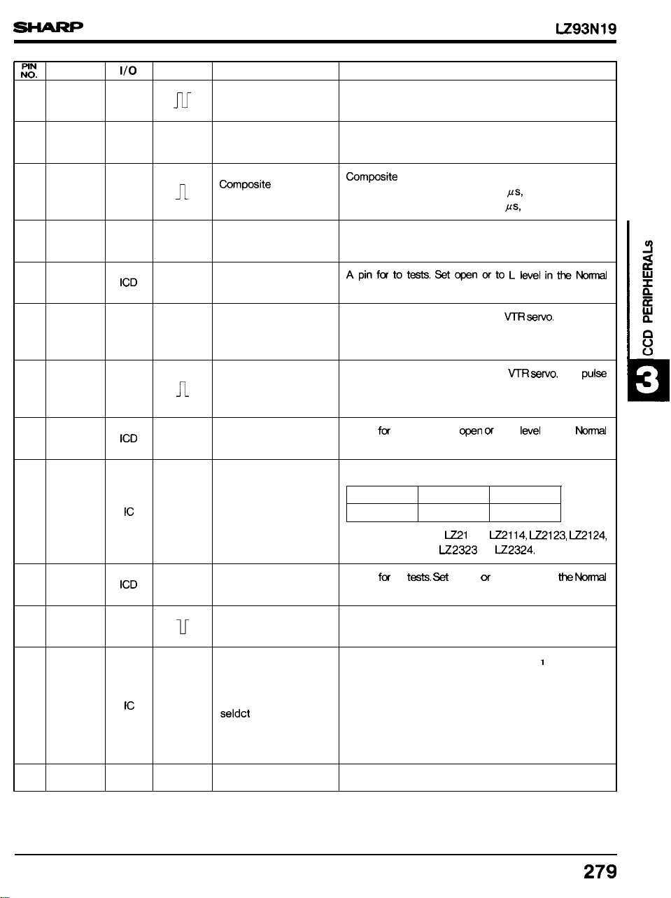
14
SYMBOL
LSW
o
POLARITY
PIN NAME
Line switch
FUNCTION
The signal switches between H and L at every line.
It is set at Low level at the 1st line of the 1st field.
15
ENCP
16 CBLK
17
CSYNC
TST5
18
19 FRP2
FRPI
20
21
TST2
22 CKMD
o
n
o
o
o
o
v
n
Encoder DC clamp
blanking
pulse
Composite synchronous
signal
—
Test terminal 5
Frame read pulse 2
Frame read pulse 1 occurs at odd fields and its repetition is frame
—
Test terminal 2
—
Clock mode select
A clamp pulse that is used for recovering DC level.
The repetition is horizontal frequency.
In NTSC mode; H : 11.01 ps, V : 20 H period
In PAL mode
A composite synchronous signal.
totests,
mode.
A clock output that is used for VTR =rvo. The pulse
occurs at even fields and its repetition is frame
period.
A clock output that is used for VTR
period.
A pin
mode.
A pin to select the factor of frequeny divisions,
Set to L level for
U2313, LZ2314, LZ2323 or
to tests. Set
Division
CKMD
; H : 12.12
1/3 1/4
LOW
13, LZ2114,
V : 25 H period
to L Iwel in the
HIGH
The PUIS
TST4
23
24
HBLK
25 CPMD
GND
26
o
– –
– Test terminal 4
Horizontal blanking A pulse that corresponds to the cease period of
pulse
Clamp Pulse mode
—
Grounding
A pin
mode.
the horizontal transfer pulse.
An input pin to stop or continue BCP
BCP2 (pin 38) pulses within the vertical blanking
period.
A grounding pin.
to
open
to L level in
L level : continuous output.
H level : becomes Low level during the ab-
sence of effective pixels within V
blanking period.
(pin 37) and
Page 5
SYMBOL
27 CLKI
PIN NAME
Main clock
FUNCTION
An input pin for reference clock,
to DOUT (pin 3) of timing LSI (U93N61 ) or
DO (pin 3) of timing LSI; following frequencies appear on this pin;
At
mode : 9.534964 MHz when CKMD = L level
12.713285 MHz when CKMD = H level
At PAL mode : 9.656250 MHz when CKMD = L level
12.875
MHz when CKMD = H level
28
29
30
31
32
33
Vcc
HD
RPI
SCHD
— —
TO
o
o
Power supply
Phase comparator
—
output
Horizontal comparison
input
Horizontal drive pulse
Horizontal reference the phase comparator. Connect to HD (pin 31) when
input
Subcarrier HD
Supply +5 V
Phase comparator output for input signals RPI (pin
32) and
is Low level. When CPI is delayed, output is High
level, When phases are equal, the terminal impedance is High.
An input pin for comparison horizontal signal to the
phase comparator. Connect to SCHD (pin 33) when
comparator is used. Set to L level when comparator
is not used.
The pulse occurs at the start of lines. Connect to
timing LSI.
An input pin for the reference horizontal signal to
comparator is used, Set to L level when comparator
is not used.
A horizontal synchronization pulse obtained by dividing 4FSC (pin 43).
At NTSC mode : dividing into 1 /91 O 4FSC.
At PAL mode : dividing into
(pin 30). When
narily and dividing into 1/1 137
4FSC during one horizontal period within the V blanking,
is advanced, output
135 4FSC ordi-
34
35
36
VD
CPBL
The pulse occurs at the start of every field. Con-
0
o
V drive pulse
Filed index 2nd field; HIGH
Blanking clamp pulse
nect to VDI (pin 2) of timing
of timing
(Pin
The pulse is used for detecting field.
At NTSC mode : 1st field; LOW
At PAL mode : 1st and 3rd field; LOW
When the input is High, BCPI (pin 37) and BCP2
(pin 36) are Low.
(U92E62).
2nd and 4th field; HIGH
) or VDI
Page 6

PIN
37
SYMBOL
BCP
POLARITY
I
o
n
Optical black
clamp pulse 1 and CPBL is Low, output stays Low during the ab-
NAME
FUNCTION
A pulse to clamp the optical black signal. This pulse
is continuous at horizontal cycle when CPMD (pin
25) and CPBL (pin 36) are Low.
sence of effective pixels within the Vertical blanking, otherwise is continuous at horizontal cycle.
CPMD is High
BCP2
38
PBLK
39
40
41
42 WBLK
43 4FSC
44
—
Optical black
clamp pulse 2 is delayed by 900 ns from BCP
output
Line index pulse 1
Line index pulse 2
Wide blanking pulse
4FSC input
Test terminal 1
o
o
I
o
o
n
n
o
BCP2 is
Equivalent to CBLK (pin 16) pulse except for shorter
pulse width with cut-off trailing edge.
The pulse is used in color separator. The signal
switches H and L at every line. It resets at the
14th line when in NTSC, and at the 9th line when
in PAL mode.
The pulse is used in color separator. The signal
switches H and L at every line. It resets at the
277th line when in NTSC, and at the 322th line
when in PAL mode.
Equivalent to CBLK (pin 16) except that its pulse
width is wider than that of CBLK.
An input pin for the signal 4 times the color
carrier frequeny.
Connect to L level, when
5) signals are not required.
A pin for tests. Set open or to L level in the Normal
mode.
as BCPI (pin 37) except that BCP2
1.
At NTSC mode : 14,318180 MHz
At PAL mode : 17.734475 MHz
: Input pin (CMOS level).
ICU : Input pin (CMOS level with pull-up resistor).
: Input pin (CMOS level with pull-down resistor).
o
TO :
:
:
Output pin.
Input pin (CMOS level with pull-up resistor)
output pin.
281
Page 7
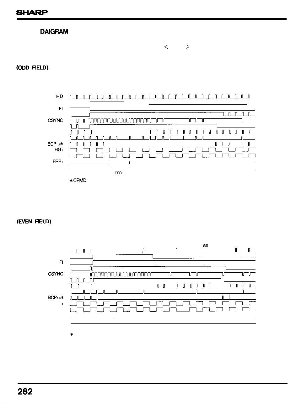
TIMING
LZ93N19
VERTICAL TIMING < NTSC
5235245251 234 56789101112131415 16171619202122232425
VD
CBLK
PBLK
BF
WHD
HG2
CFMO
HD
VD
CBLK
PBLK
BF
HD
HG
HG2
FRP2
CFMO
n
n n
u
u u u u
u
n
n
u u
n
n n
n
n
n
n n
n
1/2
Field
= H
260261262263264265266 267266269270271272273 274275276277276279
n n
n
n n
n
n n n n
n
n
n n
uuu
n
n n n n n n
n n n
n
nnnnn
n
n n n n n
261262 2832642652% 267
n n
n n
u u
n n n
n
r
I
u
u u u
n
n n
n
u u
mnn
n n n
n n n
n
n n
n
n n
u u H
n
n
n
n
n
n n
n n
CPMD = H
Page 8
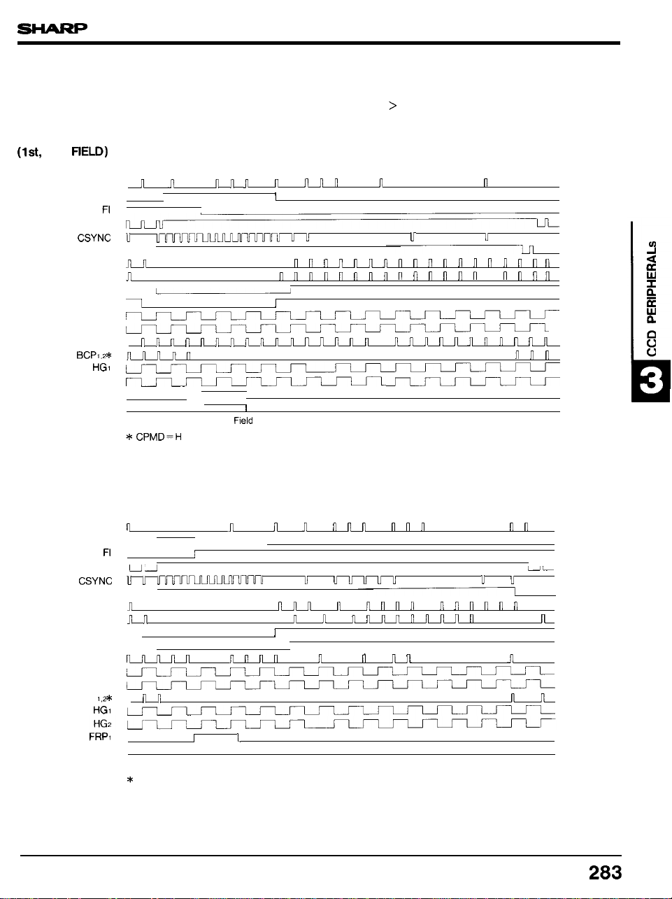
3rd flELD)
HD
VD
621622623624625
n n n
I
VERTICAL TIMING < PAL >
23456789101112 1314151617181920212223 24
n n
n n
n n
n
n
n
n n
n
n
LZ93N19
n
n
n
n
n
CBLK
PBLK
BF (1)
BF (3)
BFBL (1)
BFBL (3)
LSW (1)
LSW (3)
WHD
HG2
FRPI
CFMO
(2nd, 4th FIELD)
HD
VD
CBLK
PBLK
BF (2)
BF (4)
BFBL (2)
BFBL (4)
LSW (2)
LSW (4)
WHD
BCP
u
u
u
u u uuu
uuu
u
uuu
n
n
I
[
1/2 1st
30931031 1312313314315316317318319320321 322323324325326327328329330331 332333324335336337
. .
n n
n
n
n
n n
n
u u
1
n
n
n
n
n
I
n n
n n
u
n
n
n
n
n
n n n
n n
n
,
u
u u
n
n
n n
n
n n
n
n
n
n
nnn
u u u
u
u
n
n n
n
n
n
n
CFMO
CPMD = H
Page 9
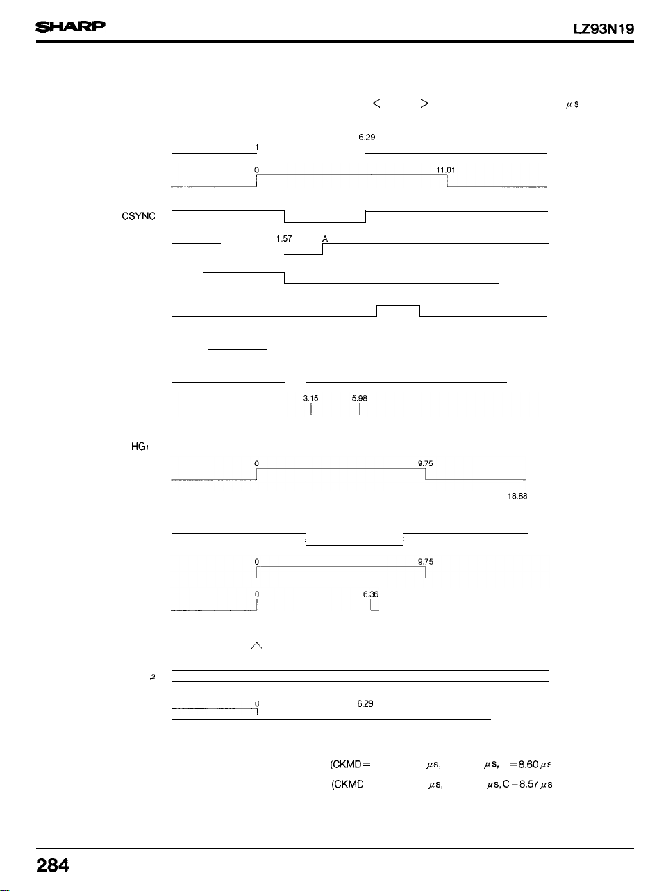
HORIZONTAL TIMING < NTSC > Unit :
HD
CBLK
(EQ)
(SAW)
BF
BCPI
BCP2
ENCP
PBLK
WBLK
HBLK
o
1
–3,15
157
1,57
629
6.92 9,44
079 2.05
1,57 2.s3
2
629
–787
B
c
WHD
SCHD
VD
FRPI
o
CFMO
NOTES :
● Applied to the CCD of 542 horizontal pixels
. Applied to the CCD of 762 horizontal pixels
= L) A = 2.31
= H) A =2.36
B = 2.94
B = 2.91
C =8.60
C=8.57
Page 10
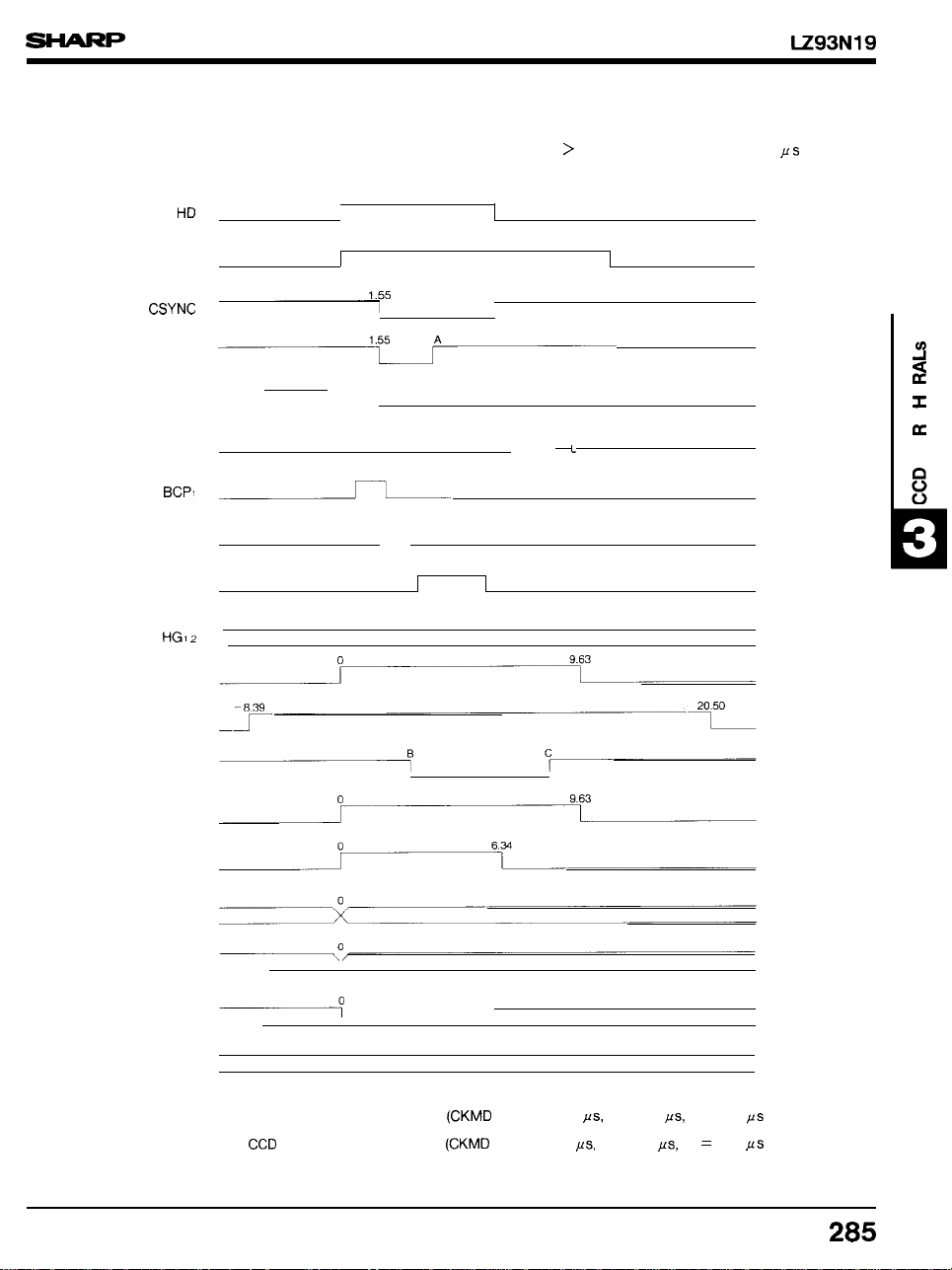
HORIZONTAL TIMING < PAL
Unit :
CBLK
(EQ)
(SAW)
BCP2
ENCP
PBLK
WBLK
HBLK
o
o
1.55
–311
BF
155
078 280
155 280
310 590
6,21
12,12
621
714 932
WHD
SCHD
VD
FRPI 2
CFMO
LSW
1,55
6,21
NOTES :
● Applied to the CCD of 542 horizontal pixels (CKMD = L) A = 2.28 PS, B = 2.90
● Applied to the
B = 2.87
C = 9.73 PS
C
9.70 ES
Page 11
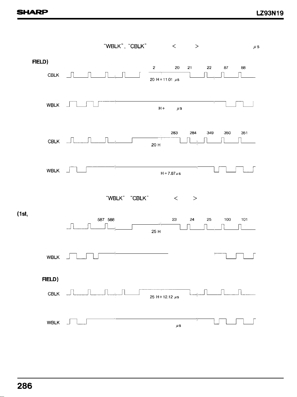
TIMING < NTSC > Unit : ps
(ODD
(EVEN FIELD)
3rd FIELD)
CBLK
492 493 525
230
231
232
263 264
n
,
586
623 624
n
1
118.5
18.88
118.5
TIMING < PAL >
349 350
100
351
101
(2nd, 4th HELD)
274 275 276 310
137.5 H +20.51 US
311
137.5 H +8.39 X5
412 413 414
336
 Loading...