

Page 1
3.3V-5V 1 Mbit (128Kb x8) TIMEKEEPERSRAM
■ INTEGRATED ULTRA LOW POWER SRAM,
REAL TIME CLOCK, POWER-FAIL CONTROL
CIRCUIT, BATTERY ANDCRYSTAL
■ YEAR 2000 COMPLIANT
■ BCD CODED CENTURY, YEAR, MONTH,
DAY, DATE, HOURS, MINUTES, and
SECONDS
■ BATTERY LOW WARNING FLAG
■ AUTOMATIC POWER-FAIL CHIP DESELECT
and WRITE PROTECTION
■ TWO WRITE PROTECT VOLTAGES:
(V
= Power-fail Deselect Voltage)
PFD
– M48T129Y: 4.2V ≤ V
– M48T129V: 2.7V ≤ V
■ CONVENTIONAL SRAM OPERATION;
UNLIMITED WRITE CYCLES
■ SOFTWARE CONTROLLED CLOCK
CALIBRATION for HIGH ACCURACY
APPLICATIONS
■ 10 YEARS of DATA RETENTION and CLOCK
OPERATION in the ABSENCE of POWER
■ SELF CONTAINED BATTERY and CRYSTAL
in DIP PACKAGE
■ MICROPROCESSOR POWER-ON RESET
(Valid even during battery back-up mode)
■ PROGRAMMABLE ALARM OUTPUT ACTIVE
in BATTERY BACK-UP MODE
■ SURFACE MOUNT CHIP SET PACKAGING
INCLUDES a 44-PIN SOIC and a 32-LEAD
TSOP (SNAPHAT TOP TO BE ORDERED
SEPARATELY)
■ SOIC PACKAGE PROVIDES DIRECT
CONNECTION for a SNAPHAT TOP WHICH
CONTAINS the BATTERY and CRYSTAL
■ SNAPHAT
HOUSING (BATTERY/CRYSTAL)
IS REPLACEABLE
PFD
PFD
≤ 4.5V
≤ 3.0V
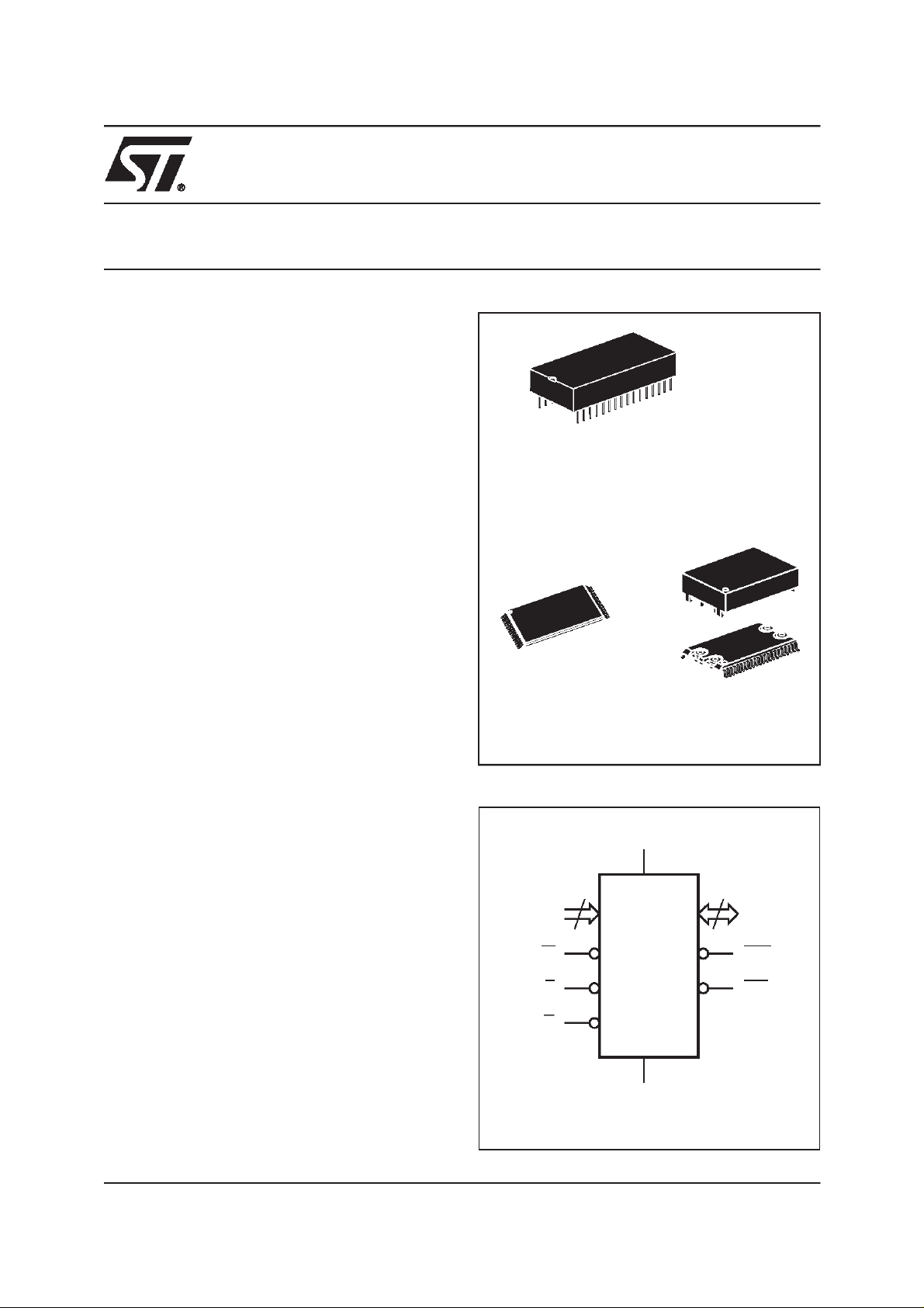
M48T129Y
M48T129V
32
1
PMDIP32(PM)
Module
SNAPHAT (SH)
Battery
TSOP32
(8 x 20mm)
Surface Mount Chip Set Solution (CS)
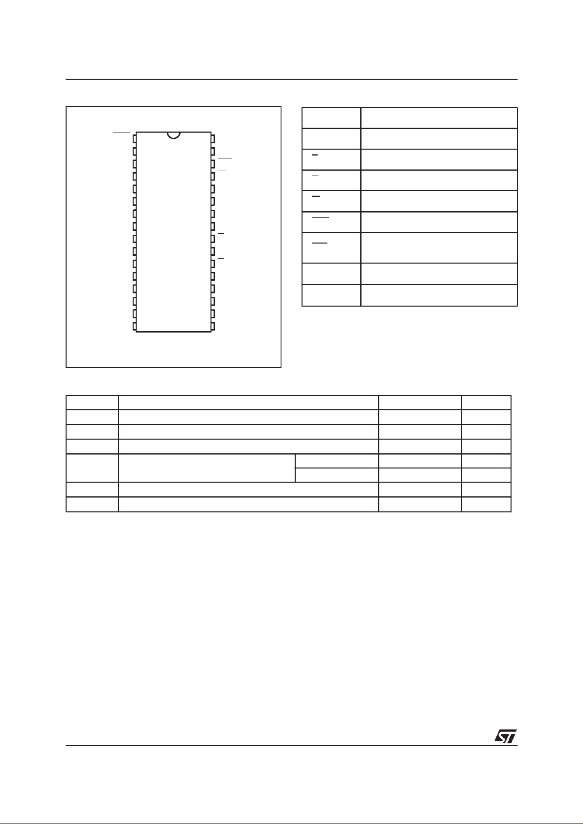
Figure 1. Logic Diagram
V
CC
17
A0-A16 DQ0-DQ7
W RST
E
G
M48T129Y
M48T129V
SOH44
8
IRQ/FT
V
SS
AI02260
1/22April 2000
Page 2
M48T129Y, M48T129V
Figure 2. DIP Connections
RST V
1
A16
2
A14
A12
4
A7
5
A6
6
A5
7
A4
8
M48T129Y
A3
A2
A1
A0
DQ0
M48T129V
9
10
11
12
13
14
DQ2
15
16
SS
Table 2. Absolute Maximum Ratings
Symbol Parameter Value Unit
T
A
T
STG
V
IO
V
CC
I
O
P
Note: 1. Stresses greater than those listed under ”Absolute Maximum Ratings” may cause permanent damage to the device. Thisis a stress
2. Soldering temperature not to exceed 260°C for 10 seconds (total thermal budget not to exceed 150°C for longer than 30 seconds).
CAUTION: Negative undershoots below –0.3V are not allowed on any pin while in the Battery Back-up mode.
Ambient Operating Temperature 0 to 70 °C
Storage Temperature (VCCOff, Oscillator Off)
Input or Output Voltages
Supply Voltage
Output Current 20 mA
Power Dissipation 1 W
D
rating only and functional operation of the device at these or any other conditions above those indicated in the operational section
of this specification is not implied. Exposure to the absolute maximum rating conditions for extended periods of time may affect
reliability.
32
31
30
29
28
27
26
25
24
23
22
21
20
19
18
17
AI02261
CC
A15
IRQ/FT3
W
A13
A8
A9
A11
G
A10
E
DQ7
DQ6
DQ5DQ1
DQ4
DQ3V
(1)
Table 1. Signal Names
A0-A16 Address Inputs
DQ0-DQ7 Data Inputs / Outputs
E Chip Enable Input
G Output Enable Input
W Write Enable Input
RST Reset Output (open drain)
IRQ/FT
V
CC
V
SS
M48T129Y –0.3 to 7.0 V
M48T129V –0.3 to 4.6 V
Interrupt / Frequency Test Output
(open drain)
Supply Voltage
Ground
–40 to 85 °C
–0.3 to V
CC
+0.3
V
DESCRIPTION
The M48T129Y/V TIMEKEEPER RAM is a 128Kb
x 8 non-volatile static RAM and real time clock,
with programmable alarms and a watchdog timer.
The special DIP package provides a fully integrated battery back-up memoryandrealtime clock solution. The M48T129Y/V directly replaces industry
standard 128Kb x 8 SRAM. It also provides the
non-volatility of Flash without any requirement for
special write timing or limitations on the number of
writes that can be performed.
2/22
For surface mount environments ST provides a
Chip Set solution consisting of a 44 pin 330mil
SOIC TIMEKEEPER Supervisor (M48T201V/Y)
and a 32 pin TSOP (8 x 20mm) LPSRAM
(M68Z128/W) packages.
The 44 pin 330mil SOIC provides sockets with
gold plated contacts at both ends for direct connection to a separate SNAPHAT housing containing the battery.
The unique design allows the SNAPHAT battery
package to be mounted on top of the SOIC package after the completion of the surface mount pro-
Page 3
Figure 3. Block Diagram
M48T129Y, M48T129V
AND
V
CC
AND
POWER
SENSE
32,768
Hz
CRYSTAL
LITHIUM
CELL
OSCILLATOR
CLOCK CHAIN
VOLTAGE
SWITCHING
CIRCUITRY
cess. Insertion of the SNAPHAT housing after
reflow prevents potential battery damage due to
the hightemperatures required for device surfacemounting. The SNAPHAT housing is keyed to prevent reverse insertion.
The SNAPHAT battery package is shipped separately in plastic anti-static tubes or in Tape & Reel
form. The part number is ”M4Txx-BR12SH1”.
The 32 pin 600 mil DIP Hybrid houses a controller
chip, SRAM, quartz crystal, and a long life lithium
button cell in a single package.
Figure 3 illustratesthestaticmemoryarray andthe
quartz controlled clock oscillator. The clock locations contain the century, year, month, date, day,
hour, minute, and second in 24 hour BCD format.
Corrections for 28, 29 (leap year), 30, and 31 day
months are made automatically. The nine clock
bytes (1FFFFh-1FFF9h and 1FFF1h) are not the
actual clock counters, they are memory locations
consisting of BiPORT read/write memory cells
within the static RAM array.
The M48T129Y/V includes a clock control circuit
which updates the clock bytes with current information once per second. The information can be
accessed by the user in the same manner as any
other location in the static memory array. Byte
16 x 8
TIMEKEEPER
REGISTERS
RST
IRQ/FT
A0-A16
DQ0-DQ7
E
W
G
AI02583
V
PFD
131,056 x 8
SRAM ARRAY
V
SS
1FFF8his the clock control register.Thisbyte controls user access to the clock information and also
stores the clock calibration setting.
Byte 1FFF7h contains the watchdog timer setting.
The watchdog timer can generate either a reset or
an interrupt, depending on the state of the WatchdogSteering bit(WDS).Bytes 1FFF6h-1FFF2h include bits that, when programmed, provide for
clock alarm functionality. Alarms are activated
when the register content matches the month,
date, hours, minutes, and seconds of the clock
registers. Byte 1FFF1h contains century information.Byte 1FFF0h contains additionalflaginformation pertaining to the watchdog timer, the alarm
condition and the battery status. The M48T129Y/V
also has its own Power-Fail Detect circuit. This
control circuitry constantly monitors the supply
voltage for an out of tolerance condition. When
VCCis out of tolerance, the circuit write protects
the TIMEKEEPER register data and external
SRAM, providing data security in the midst of unpredictable system operation. As VCCfalls, the
control circuitry automatically switches to the battery, maintaining data and clock operation until
valid power is restored.
3/22
Page 4
M48T129Y, M48T129V
Figure 4. Hardware Hookup for SMT Chip Set
Hz
LITHIUM
CELL
(3)
A0-A16
M48T201Y/V
V
CC
E
W
G
WDI
RSTIN1
RSTIN2
V
SS
DQ0-DQ7
SNAPHAT
BATTERY/CRYSTAL
32,768
CRYSTAL
5V
0.1µF
(1)
V
OUT
(2)
ECON
GCON
RST
IRQ/FT
SQW
0.1µF
V
CC
M68Z128/W
E
W
G
V
SS
A0-A16
(2)
DQ0-DQ7
Note: 1. For pin connections, see individual data sheets for M48T201Y/V and M68Z128/W atwww.st.com.
2. For 5V, M48T129Y (M48T201Y + M68Z128). For 3.3V, M48T129V (M48T201V + M68Z128W).
3. SNAPHAT Top ordered separately.
READ MODE
The M48T129Y/V is in the Read Mode whenever
W (Write Enable) is high and E (Chip Enable) is
low. The unique address specified by the 17 Address Inputs defines which one of the 131,072
bytes of data is to be accessed. Valid data will be
available at the Data I/O pins within t
AVQV
(Address Access Time) after the last address input
signal is stable, providing the E and G access
times are also satisfied. If the E and G access
times are not met, valid data will be available after
the latterof the Chip Enable Access Times (t
or Output Enable Access Time (t
GLQV
ELQV
).
The state of the eight three-state Data I/O signals
is controlled by E and G. If the outputs are activated before t
indeterminate state until t
, the data lines will be driven to an
AVQV
. If the Address In-
AVQV
puts are changed while E and G remain active,
output data will remain valid for t
AXQX
(Output
Data Hold Time) but will go indeterminate until the
next Address Access.
WRITE MODE
The M48T129Y/V is in the Write Mode whenever
W (Write Enable) and E (Chip Enable) are low
state after the address inputs are stable.
The start of a write is referencedfrom the latter occurring falling edgeof W orE. A write is terminated
by the earlierrisingedge of W or E. The addresses
must be held valid throughout the cycle. E or W
)
must return high for a minimum of t
Enable or t
from Write Enable prior to the ini-
WHAX
tiation of another read or write cycle. Data-in must
be valid t
valid for t
prior to the end of write and remain
DVWH
afterward. G should be kept high
WHDX
during write cycles to avoid bus contention; although, if the output bus has been activated by a
low on E and G a low on Wwill disable the outputs
t
after W falls.
WLQZ
AI03632
EHAX
fromChip
4/22
Page 5
M48T129Y, M48T129V
≤ V
V
or
PFD
SO
CC
(1)
(min)
(2)
(2)
E G W DQ0-DQ7 Power
V
IH
V
IL
V
IL
V
IL
X X X High Z CMOS Standby
X X X High Z Battery Back-up Mode
Table 3. Operating Modes
Mode
Deselect
Write
Read
Read
Deselect
Deselect
Note: 1. X = VIHor VIL;VSO= Battery Back-up Switchover Voltage.
2. See Table 7 for details.
4.5V to 5.5V
3.0V to 3.6V
to V
V
SO
DATA RETENTION MODE
With valid VCCapplied, the M48T129Y/V operates
as a conventional BYTEWIDE static RAM.
Should the supply voltage decay, the RAM will automatically deselect, write protecting itself when
VCCfalls between V
PFD
(max), V
PFD
(min) window. All outputs become high impedance and all
inputs are treated as ”don’t care”.
Note: Apower failureduring a write cycle may corrupt data at the current addressed location, but
does not jeopardize the rest of the RAM’s content.
At voltages below V
(min), the memory will be
PFD
in a write protected state, provided the VCCfall
time is not less than tF. The M48T129Y/V may respond to transient noise spikes on VCCthat cross
into the deselect window during the time the device issampling VCC. Therefore, decouplingof the
power supply lines is recommended.
When VCCdrops below VSO, the control circuit
switches power to the internal battery, preserving
data and powering the clock. The internal energy
source will maintain data in the M48T129Y/V for
an accumulated period of at least 10 years atroom
temperature. As system power rises above VSO,
the battery is disconnected, and the power supply
is switched to external VCC. Deselect continues for
t
after VCCreaches V
REC
(max). For a further
PFD
more detailed review of lifetime calculations,
please see Application Note AN1012.
TIMEKEEPER REGISTERS
The M48T129Y/V offers 16 internal registers
which contain TIMEKEEPER, Alarm, Watchdog,
Interrupt, Flag, and Control data. These registers
are memory locations which contain external (user
accessible) andinternal copies ofthe data (usually
referred to as BiPORT TIMEKEEPER cells). The
X X High Z Standby
X
V
IL
V
IH
V
IL
V
IH
V
IH
D
IN
D
OUT
High Z Active
Active
Active
Table 4. AC Measurement Conditions
Input Rise and Fall Times ≤ 5ns
Input Pulse Voltages 0 to 3V
Input and Output Timing Ref. Voltages 1.5V
Note thatOutput Hi-Z is defined as the point wheredata is no longer
driven.
Figure 5. AC Testing Load Circuit
DEVICE
UNDER
TEST
CLincludes JIG capacitance
Note: Excluding open drain output pins
650Ω
CL= 100pF
1.75V
AI01803C
external copies are independent of internal functions except that they are updated periodically by
the simultaneoustransferof theincrementedinternal copy. TIMEKEEPER and Alarm Registers
store data in BCD.
5/22
Page 6

M48T129Y, M48T129V
CLOCK OPERATIONS
Reading the Clock
Updates to the TIMEKEEPER registers should be
halted beforeclock data is read to prevent reading
data in transition. Because the BiPORT TIMEKEEPER cellsin the RAM array are only data registers, and not the actual clock counters, updating
the registers can be halted without disturbing the
clock itself.
Updating is halted when a ’1’ is written to the
READ bit, D6 in the Control Register (1FFF8h). As
long as a ’1’ remains in that position, updating is
halted. After a halt is issued, the registers reflect
the count;thatis,the day,date, and time that were
current at the moment the halt command was issued. All ofthe TIMEKEEPER registers are updated simultaneously. A halt will not interrupt an
update in progress. Updating occurs 1 second after the READ bit is reset to a’0’.
Setting the Clock
Bit D7 of the Control Register (1FFF8h) is the
WRITE bit. Setting the WRITE bit to a ’1’, like the
READ bit, halts updates to the TIMEKEEPER registers. The user can then load them with the correct day, date, and time data in 24 hour BCD
format (see Table 11).
Resetting the WRITE bit to a ’0’then transfers the
values of all time registers (1FFFFh-1FFF9h,
1FFF1h) to theactual TIMEKEEPER counters and
allows normal operation to resume. After the
WRITE bit isreset, thenextclockupdate willoccur
approximately one second later.
Note: Upon power-up following a power failure,
both the WRITE bit and the READ bit will be reset
to ’0’.
Stopping and Starting the Oscillator
The oscillator may be stopped at any time. If the
device is going to spend a significant amount of
time on the shelf, the oscillator can be turned off to
minimize current drain on the battery. The STOP
bit is located at Bit D7 within 1FFF9h. Setting it to
a ’1’ stops the oscillator. When reset to a ’0’, the
M48T129Y/V oscillator starts within one second.
Note: It is not necessary to set the WRITE bit
when setting or resetting the FREQUENCY TEST
bit (FT) or the STOP bit (ST).
SETTING ALARM CLOCK
Registers 1FFF6h-1FFF2h contain the alarm settings. The alarm can be configured to go off at a
prescribed time on a specific month, date, hour,
minute, or second or repeat every month, day,
hour, minute, or second. It can also be programmed to go off while the M48T129Y/V is in the
battery back-upto serveasa systemwake-upcall.
Bits RPT5-RPT1 putthe alarm in the repeat mode
of operation. Table 12 shows the possible configurations.Codes not listedin the tabledefaultto the
once per second mode toquickly alert the user of
an incorrect alarm setting.
Note: User must transition address (or toggleChip
Enable) to see Flag Bit change.
When the clock information matches the alarm
clock settings based on the match criteria defined
by RPT5-RPT1, the AF (Alarm Flag)is set. If AFE
(Alarm Flag Enable) is also set, the alarm condition activates the IRQ/FT pin. To disable alarm,
write ’0’ to the Alarm Date register and RPT1-4.
The IRQ/FT output is cleared by a read to the
Flags register as shown in Figure 12. A subsequent read of the Flags register will reset the
Alarm Flag (D6; Register 1FFF0h).
The IRQ/FT pin can also be activated in the battery back-up mode. The IRQ/FT will go low if an
alarm occurs and both ABE (Alarm in Battery
Back-up Mode Enable)and AFE areset. The ABE
and AFE bits are reset during power-up, therefore
an alarm generated during power-up will only set
AF. Theuser can read the Flag Register at system
boot-up to determine if an alarm was generated
while the M48T129Y/V was in the deselect mode
during power-up. Figure 13 illustratesthe back-up
mode alarm timing.
6/22
Page 7
M48T129Y, M48T129V
Table 5. Capacitance
(1)
(TA=25°C, f = MHz)
Symbol Parameter Test Condition Min Max Unit
C
IN
C
IO
Note: 1. Effective capacitance measured with power supply at 5V (M48T129Y) or 3.3V (M48T129V). Sampled only, not 100% tested.
2. Outputs deselected.
Input Capacitance
(2)
Input / Output Capacitance
V
V
OUT
IN
=0V
=0V
20 pF
20 pF
Table 6A. DC Characteristics
(TA= 0 to 70 °C; VCC= 4.5V to 5.5V)
Symbol Parameter Test Condition Min Max Unit
(1)
I
LI
I
LO
I
I
I
V
V
V
Note: 1. Outputs deselected.
Input Leakage Current 0V ≤ VIN≤ V
(1)
Output Leakage Current
Supply Current Outputs open 95 mA
CC
Supply Current (Standby) TTL
CC1
Supply Current (Standby) CMOS
CC2
Input Low Voltage –0.3 0.8 V
V
IL
Input High Voltage 2.2
IH
Output Low Voltage
OL
Output High Voltage
OH
0V ≤ V
E=V
I
OL
I
OH
OUT
E=V
CC
= 2.1mA
= –1mA
CC
≤ V
IH
–0.2V
CC
2.4 V
±2 µA
±2 µA
8mA
4mA
V
CC
+ 0.3
V
0.4 V
Table 6B. DC Characteristics
(TA= 0 to 70 °C; VCC= 3.0V to 3.6V)
Symbol Parameter Test Condition Min Max Unit
(1)
I
LI
I
LO
I
I
I
V
V
V
Note: 1. Outputs deselected.
Input Leakage Current
(1)
Output Leakage Current
Supply Current Outputs open 50 mA
CC
Supply Current (Standby) TTL E = V
CC1
Supply Current (Standby) CMOS
CC2
Input Low Voltage –0.3 0.4 V
V
IL
Input High Voltage 2.2
IH
Output Low Voltage IOL= 2.1mA 0.4 V
OL
Output High Voltage
OH
0V ≤ V
0V ≤ V
E=V
I
OH
≤ V
IN
≤ V
OUT
IH
–0.2V
CC
= –1mA
CC
CC
±2 µA
±2 µA
4mA
3mA
V
+ 0.3
CC
2.2 V
V
7/22
Page 8

M48T129Y, M48T129V
Figure 6. Power Down/Up Mode AC Waveforms
V
CC
V
(max)
PFD
V
(min)
PFD
V
SO
tF
tFB
INPUTS
tRB
DON’T CARE
tR
tREC
RECOGNIZEDRECOGNIZED
OUTPUTS
RST
VALID VALID
Table 7. Power Down/Up Trip Points DC Characteristics
HIGH-Z
AI01805
(1)
(TA= 0 to 70 °C)
Symbol Parameter Min Typ Max Unit
V
PFD
Power-fail Deselect Voltage
M48T129Y 4.2 4.35 4.5 V
M48T129V 2.7 2.9 3.0 V
M48T129Y 3.0 V
V
SO
t
DR
Note: 1. All voltages referenced to VSS.
2. At 25°C.
Battery Back-up Switchover Voltage
V
M48T129V
(2)
Expected Data Retention Time 10 YEARS
PFD
–100mV
Table 8. Power Down/Up AC Characteristics
(TA= 0 to 70 °C)
Symbol Parameter Min Max Unit
(1)
t
F
t
FB
t
R
t
RB
t
REC
Note: 1. V
2. V
V
(max) to V
PFD
(2)
V
(min) to VSSVCCFall Time
PFD
V
(min) to V
PFD
VSStoV
V
(max) to V
PFD
(min).
V
PFD
(min) to VSSfall time of less than tFBmay cause corruption of RAM data.
PFD
PFD
(max) to RST High
PFD
(min) falltime of lessthan tFmayresult indeselection/write protection notoccurring until50µs after VCCpasses
PFD
(min) VCCFallTime
PFD
(max) VCCRise Time
PFD
(min) VCCRise Time
300 µs
M48T129Y 10 µs
M48T129V 150 µs
10 µs
1 µs
40 200 ms
V
8/22
Page 9

Table 9. Read Mode AC Characteristics
(TA= 0 to 70 °C)
Symbol Parameter
t
AVAV
t
AVQV
t
ELQV
t
GLQV
t
ELQX
t
GLQX
t
EHQZ
t
GHQZ
t
AXQX
Note: 1. CL= 100pF.
2. C
Read Cycle Time 70 85 ns
(1)
Address Valid to Output Valid 70 85 ns
(1)
Chip Enable Low to Output Valid 70 85 ns
(1)
Output Enable Low to Output Valid 40 55 ns
(2)
Chip Enable Low to Output Transition 5 5 ns
(2)
Output Enable Low to Output Transition 5 5 ns
(2)
Chip Enable High to Output Hi-Z 25 30 ns
(2)
Output Enable High to Output Hi-Z 25 30 ns
(1)
Address Transition to Output Transition 5 5 ns
= 5pF.
L
M48T129Y, M48T129V
M48T129Y M48T129V
Unit-70 -85
Min Max Min Max
Figure 7. Address Controlled, Read Mode AC Waveforms
tAVAV
A0-A16
DQ0-DQ7
tAVQV
tAXQX
DATA VALID
VALID
DATA VALID
AI02324
9/22
Page 10

M48T129Y, M48T129V
Table 10. Write Mode AC Characteristics
(TA= 0 to 70 °C)
M48T129Y M48T129V
Symbol Parameter
Min Max Min Max
t
AVAV
t
AVWL
t
AVEL
t
WLWH
t
ELEH
t
WHAX
t
EHAX
t
DVWH
t
DVEH
t
WHDX
t
EHDX
t
WLQZ
t
AVWH
t
AVEH
t
WHQX
Note: 1. CL= 5pF.
2. If E goes low simultaneously with W going low, the outputs remain in the high impedance state.
Write Cycle Time 70 85 ns
Address Valid to Write Enable Low 0 0 ns
Address Valid to Chip Enable Low 0 0 ns
Write Enable Pulse Width 50 60 ns
Chip Enable Low to Chip Enable High 55 65 ns
Write Enable High to Address Transition 5 5 ns
Chip Enable High to Address Transition 10 15 ns
Input Valid to Write Enable High 30 35 ns
Input Valid to Chip Enable High 30 35 ns
Write Enable High to Input Transition 5 5 ns
Chip Enable High to Input Transition 10 15 ns
(1, 2)
Write Enable Low to Output Hi-Z 25 30 ns
Address Valid to Write Enable High 60 70 ns
Address Valid to Chip Enable High 60 70 ns
(1, 2)
Write Enable High to Output Transition 5 5 ns
Unit-70 -85
WATCHDOG TIMER
The watchdog timer can be used to detect an outof-control microprocessor. The user programs the
watchdog timer by setting the desired amount of
time-out into the Watchdog Register, address
1FFF7h. Bits BMB4-BMB0 store abinary multiplier
and the two lower order bits RB1-RB0 select the
resolution, where 00 = 1/16 second, 01 = 1/4 second, 10 = 1 second, and 11 = 4 seconds. The
amount of time-out is then determined to be the
multiplication of the five bit multiplier valuewiththe
resolution. (For example: writing 00001110 in the
Watchdog Register = 3*1 or 3 seconds).
Note: Accuracy of timer is within ± the selected
resolution.
If theprocessor does not reset the timer withinthe
specified period, the M48T129Y/V sets the WDF
(Watchdog Flag) and generates a watchdog interrupt or a microprocessor reset. WDF is reset by
reading the FlagsRegister (Address1FFF0h). The
most significant bitof the Watchdog Register is the
Watchdog Steering Bit (WDS). When set to a ’0’,
10/22
the watchdog will activate the IRQ/FT pin when
timed-out. When WDS is set to a ’1’, the watchdog
will output a negative pulse on the RST pin for 40
to 200 ms. The Watchdog register and the FT bit
will reset to a ’0’atthe end of aWatchdog time-out
when the WDS bit is set to a ’1’.Thewatchdogtimer can be reset by having the original time-outperiod re-written into the Watchdog Register,
effectively restarting the count-down cycle.
Should the watchdog timer time-out,and theWDS
bit is programmed to output an interrupt, a value of
00h needs to be written to the Watchdog Register
in order to clear the IRQ/FT pin. This will also disable the watchdog function until it is again programmed correctly. A read of the Flags Register
will reset the Watchdog Flag (Bit D7; Register
1FFF0h). The watchdog function is automatically
disabled upon power-down and the Watchdog
Register is cleared. If the watchdog function is set
to output to the IRQ/FT pin and the frequency test
function is activated, the watchdog or alarm function prevails and the frequency test function is denied.
Page 11

M48T129Y, M48T129V
Figure 8. Chip Enable or Output Enable Controlled, Read Mode AC Waveforms
tAVAV
A0-A16
tAVQV tAXQX
tELQV
E
tELQX
G
tGLQX
DQ0-DQ7
VALID
tGLQV
Figure 9. Write Enable Controlled, Write AC Waveforms
tEHQZ
tGHQZ
DATA OUT
AI01197
A0-A16
tAVEL
E
tAVWL
W
tWLQZ
DQ0-DQ7
tAVAV
VALID
tAVWH
tWLWH
tDVWH
tWHAX
tWHQX
tWHDX
DATA INPUT
AI02382
11/22
Page 12

M48T129Y, M48T129V
Figure 10. Chip Enable Controlled, Write AC Waveforms
A0-A16
tAVEL
E
tAVWL
W
DQ0-DQ7
POWER-ON RESET
The M48T129Y/V continuously monitors VCC.
When VCCfalls to the power fail detect trip point,
the RSTpulls low (open drain) and remains low on
power-up for 40 to 200ms after VCCpasses V
PFD
The RST pin is an open drain output and an appropriate pull-up resistor to VCCshould be chosen to
control the rise time.
CALIBRATING THE CLOCK
The M48T129Y/V is driven by a quartz controlled
oscillator with a nominal frequency of 32,768Hz.
The devices are factory calibrated at 25°C and
tested for accuracy. Clock accuracy will not exceed 35 ppm (parts per million) oscillator frequency error at 25°C, which equates to about * 1.53
minutes per month. When the Calibration circuit is
properly employed, accuracy improves to better
than +4 ppm at 25°C. The oscillation rate of crystals changes with temperature. The M48T129Y/V
design employs periodic counter correction. The
calibration circuit adds or subtracts counts from
the oscillator divider circuit at the divide by 256
stage, as shown in Figure 11.
The number of times pulses which are blanked
(subtracted, negative calibration) or split (added,
positive calibration) depends upon the value loaded intothefive Calibrationbits found in the Control
Register. Adding counts speeds the clock up, subtracting counts slows the clock down.The Calibra-
tAVAV
VALID
tELEH
DATA INPUT
tDVWH
tEHAX
tWHDX
AI02582
tion bits occupy the five lower orderbits (D4-D0) in
the Control Register 1FFF8h. These bits can be
set to represent any value between 0 and 31 in binary form. Bit D5 is a Sign bit; ’1’indicates positive
calibration, ’0’ indicates negative calibration. Cali-
.
bration occurs within a 64 minute cycle. The first
62 minutes in the cycle may, once per minute,
have one second either shortened by 128 or
lengthened by 256 oscillator cycles. If a binary ’1’
is loaded into the register, only the first 2 minutes
in the 64 minute cycle will be modified; if a binary
6 is loaded, the first 12 will be affected, and so on.
Therefore, each calibration step has the effect of
adding 512 or subtracting 256 oscillator cycles for
every 125, 829, 120 actual oscillator cycles, that is
+4.068 or –2.034 ppm of adjustment per calibration step in the calibration register. Assuming that
the oscillator is running at exactly 32,768Hz, each
of the 31 increments in the Calibration byte would
represent +10.7 or –5.35 seconds per month
which correspondstoatotal range of +5.5 or –2.75
minutes per month. Figure 11 illustrates a TIMEKEEPER calibration waveform.
Two methods are available for ascertaining how
much calibration a given M48T129Y/V may require. The first involves setting the clock, letting it
run for a month and comparing it to a known accurate reference and recording deviation over a fixed
period of time.
12/22
Page 13

M48T129Y, M48T129V
Table 11. TIMEKEEPER Register Map
Address
Data
D7 D6 D5 D4 D3 D2 D1 D0
1FFFFh 10 Years Year Year 00-99
1FFFEh 0 0 0 10 M. Month Month 01-12
1FFFDh 0 0 10 Date Date Date 01-31
1FFFCh 0 FT 0 0 0 Day of Week Day 01-07
1FFFBh 0 0 10 Hours Hours (24 Hours Format) Hour 00-23
1FFFAh 0 10 Minutes Minutes Minutes 00-59
1FFF9h ST 10 Seconds Seconds Seconds 00-59
1FFF8h W R S Calibration Control
1FFF7h WDS BMB4 BMB3 BMB2 BMB1 BMB0 RB1 RB0 Watchdog
1FFF6h AFE 0 ABE Al 10M Alarm Month A Month 01-12
1FFF5h RPT4 RPT5 Al 10 Date Alarm Date A Date 01-31
1FFF4h RPT3 0 Al 10 Hours Alarm Hours AHours 00-23
1FFF3h RPT2 Alarm 10 Minutes Alarm Minutes A Minutes 00-59
1FFF2h RPT1 Alarm 10 Seconds Alarm Seconds A Seconds 00-59
1FFF1h 1000 Year 100 Year Century 00-99
1FFF0h WDF AF 0 BL Y Y Y Y Flags
Function/Range
BCD Format
Keys: S = SIGN Bit
FT = FREQUENCY TEST Bit
R = READ Bit
W = WRITEBit
ST = STOP Bit
0 = Must be set to zero
Y = ’1’or ’0’
BL = Battery Low
Figure 11. CalibrationWaveform
NORMAL
POSITIVE
CALIBRATION
NEGATIVE
CALIBRATION
AF = Alarm Flag
WDS = Watchdog Steering Bit
BMB0-BMB4 = Watchdog Multiplier Bits
RB0-RB1 = Watchdog Resolution Bits
AFE = Alarm FlagEnable
ABE = Alarm in BatteryBack-up Mode Enable
RPT1-RPT5 = Alarm Repeat Mode Bits
WDF =Watchdog Flag
AI00594B
13/22
Page 14

M48T129Y, M48T129V
Figure 12. Alarm Interrupt Reset Waveform
AD0-AD7
ACTIVE FLAG BIT
IRQ/FT
Figure 13. Back-up Mode Alarm Waveforms
V
CC
V
(max)
PFD
V
(min)
PFD
V
SO
15ns Min
ADDRESS 1FF0h
HIGH-Z
AI02581
tREC
AFE bit in InterruptRegister
AF bit in Flags Register
IRQ/FT
HIGH-Z
Calibration values, including the number of seconds lostorgained in a given period, can be found
in Application Note: TIMEKEEPER CALIBRATION. This allows the designer to give the end
user the ability to calibrate the clock as the environment requires, even if the final product is packaged in a non-user serviceable enclosure. The
designer could providea simple utility that accesses the Calibration byte.
The second approach is better suited to a manufacturing environment, and involves the use of the
IRQ/FT pin. The pin will toggle at 512Hz, when the
Stop bit (ST, D7 of 1FFF9h) is ’0’,the Frequency
Test bit (FT, D6 of 1FFFCh) is ’1’, the Alarm Flag
HIGH-Z
AI01678C
Enable bit (AFE, D7 of 1FFF6h) is ’0’, and the
Watchdog Steering bit (WDS, D7 of 1FFF7h) is ’1’
or the Watchdog Register (1FFF7h=0) is reset.
Note: A 4 second settling time must be allowed
before reading the 512Hz output.
Any deviation from 512Hz indicates the degree
anddirectionofoscillatorfrequency shift atthetest
temperature. For example, a reading of
512.010124Hz wouldindicatea+20ppmoscillator
frequency error,requiringa–10 (WR001010)tobe
loaded into the Calibration Byte for correction.
Note that setting or changing the Calibration Byte
does not affect the Frequency testoutput frequency.
14/22
Page 15

Table 12. Alarm Repeat Modes
RPT4 RPT3 RPT2 RPT1 Alarm Activated
1 1 1 1 Once per Second
1 1 1 0 Once per Minute
1 1 0 0 Once per Hour
1 0 0 0 Once per Day
1 0 0 0 Once per Month
M48T129Y, M48T129V
Figure 14. Supply Voltage Protection
V
CC
V
CC
0.1µF DEVICE
V
SS
AI02169
The IRQ/FT pin is an open drain output which requires a pull-up resistor to VCCfor proper operation. A 500-10k resistor is recommended in order
to control the rise time. The FT bit is cleared on
power-up.
BATTERY LOW WARNING
The M48T129Y/V automatically performs battery
voltage monitoring upon power-up and at factoryprogrammed time intervals of approximately 24
hours. The Battery Low (BL) bit, Bit D4 of Flags
Register 1FFF0h, will be asserted if the battery
voltage is found to be less than approximately
2.5V.
If a battery low is generated during a power-up se-
quence, this indicates that the battery is below approximately 2.5 volts and may not be able to
maintain data integrity in the SRAM. Data should
be considered suspect and verified as correct.
If a battery low indication is generated during the
24-hour interval check, this indicates that the battery is near end of life. However, data is not compromised due to the fact that a nominal VCCis
supplied.
The M48T129Y/V only monitors the battery when
a nominal VCCisapplied to the device. Thus applications which require extensive durations in the
battery back-up modeshould be powered-up periodically (at least once every few months) in order
for this technique to be beneficial. Additionally, if a
battery low is indicated, data integrity should be
verified upon power-up via a checksum or other
technique.
POWER-ON DEFAULTS
Upon application of power to the device, the following register bits are set to a ’0’ state: WDS,
BMB0-BMB4, RB0,RB1, AFE, ABE, W, R and FT.
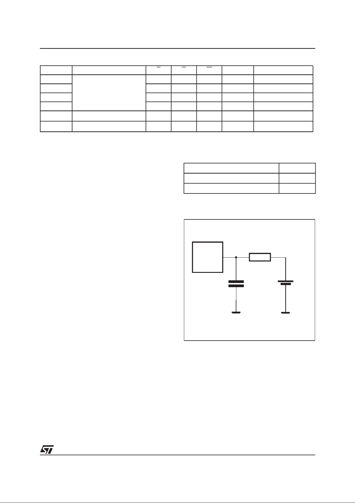
POWER SUPPLY DECOUPLING
and UNDERSHOOT PROTECTION
ICCtransients, including those produced by output
switching, can produce voltage fluctuations, resulting in spikes on the VCCbus. These transients
can be reduced if capacitors are used to store energy, which stabilizes the VCCbus. The energy
stored in the bypass capacitors will be released as
low going spikes are generated or energy will be
absorbed when overshoots occur. A ceramic bypass capacitor value of 0.1µF (see Figure 14) is
recommended in order to provide the needed filtering. In addition to transients that are caused by
normal SRAMoperation, powercyclingcangenerate negative voltage spikes on VCCthat drive it to
values below VSSby as much as one volt. These
negative spikes can cause data corruption in the
SRAM while in battery backup mode. To protect
from these voltage spikes, ST recommends connecting a schottky diodefrom VCCtoVSS(cathode
connected to VCC, anode to VSS). (Schottky diode
1N5817 is recommended for through hole and
MBRS120T3 is recommended for surface mount).
15/22
Page 16

M48T129Y, M48T129V
Table 13. Ordering Information Scheme
Example: M48T129Y -70 PM 1
Device Type
M48T
SupplyVoltage and Write Protect Voltage
129Y = V
129V = V
Speed
-70 = 70ns
-85 = 85ns
Package
PM = PMDIP32
(1)
CS
Temperature Range
1=0to70°C
= 4.5V to 5.5V; V
CC
= 3.0V to 3.6V; V
CC
= 4.2V to 4.5V
PFD
= 2.7V to 3.0V
PFD
=SurfaceMountChipSetsolution M48T201Y/V (SOH44)+ M68Z128/W (TSOP32)
Note: 1. The SOIC package (SOH44) requires the battery package (SNAPHAT) which isordered separately under the part number
”M4Txx-BR12SH1” in plastic tube or ”M4Txx-BR12SH1TR” in Tape & Reel form.
Caution: Do not place theSNAPHATbatterypackage ”M4Txx-BR12SH1” inconductive foam since thiswilldrain the lithiumbutton-cell
battery.
For a list of available options (Speed, Package, etc...) or for further information on any aspect of this device, please contact the ST Sales Office nearest to you.
Table 14. Revision History
Date Revision Details
April 2000 Chipset datasheet - First Issue
16/22
Page 17

M48T129Y, M48T129V
Table 15. PMDIP32 - 32 pin Plastic Module DIP, Package Mechanical Data
Symb
Typ Min Max Typ Min Max
A 9.27 9.52 0.365 0.375
A1 0.38 – 0.015 –
B 0.43 0.59 0.017 0.023
C 0.20 0.33 0.008 0.013
D 42.42 43.18 1.670 1.700
E 18.03 18.80 0.710 0.740
e1 2.29 2.79 0.090 0.110
e3 34.29 41.91 1.350 1.650
eA 14.99 16.00 0.590 0.630
L 3.05 3.81 0.120 0.150
S 1.91 2.79 0.075 0.110
N32 32
mm inches
Figure 15. PMDIP32 - 32 pin Plastic Module DIP, Package Outline
A1AL
S
Be1
e3
D
N
E
1
Drawing is not to scale.
C
eA
PMDIP
17/22
Page 18

M48T129Y, M48T129V
Table 16. TSOP32 - 32 lead Plastic Thin Small Outline, 8 x 20mm, Package Mechanical Data
Symbol
Typ Min Max Typ Min Max
A 1.200 0.0472
A1 0.050 0.150 0.0020 0.0059
A2 0.950 1.050 0.0374 0.0413
B 0.150 0.270 0.0059 0.0106
C 0.100 0.210 0.0039 0.0083
D 19.800 20.200 0.7795 0.7953
D1 18.300 18.500 0.7205 0.7283
e 0.500 – – 0.0197 – –
E 7.900 8.100 0.3110 0.3189
L 0.500 0.700 0.0197 0.0276
α 0° 5° 0° 5°
CP 0.100 0.0039
N32 1.3
mm inch
Figure 16. TSOP32 - 32 lead Plastic Thin Small Outline, 8 x 20mm, Package Outline
A2
1N
e
E
B
N/2
D1
D
DIE
A
CP
C
TSOP-a
Drawing is not to scale.
LA1 α
18/22
Page 19

M48T129Y, M48T129V
Table17. SH - 4-pinSNAPHAT Housing for48mAhBattery & Crystal, Package Mechanical Data
Symb
Typ Min Max Typ Min Max
A 9.78 0.385
A1 6.73 7.24 0.265 0.285
A2 6.48 6.99 0.255 0.275
A3 0.38 0.015
B 0.46 0.56 0.018 0.022
D 21.21 21.84 0.835 0.860
E 14.22 14.99 0.560 0.590
eA 15.55 15.95 0.612 0.628
eB 3.20 3.61 0.126 0.142
L 2.03 2.29 0.080 0.090
mm inches
Figure 17. SH- 4-pin SNAPHATHousing for 48 mAhBattery & Crystal, Package Outline
A1
A
eA
D
B
eB
E
SHTK-A
Drawing is not to scale.
A2
A3
L
19/22
Page 20

M48T129Y, M48T129V
Table18. SH - 4-pinSNAPHAT Housing for120 mAhBattery & Crystal, Package Mechanical Data
Symb
Typ Min Max Typ Min Max
A 10.54 0.415
A1 8.00 8.51 0.315 .0335
A2 7.24 8.00 0.285 0.315
A3 0.38 0.015
B 0.46 0.56 0.018 0.022
D 21.21 21.84 0.835 0.860
E 17.27 18.03 0.680 .0710
eA 15.55 15.95 0.612 0.628
eB 3.20 3.61 0.126 0.142
L 2.03 2.29 0.080 0.090
mm inches
Figure 18. SH- 4-pin SNAPHATHousing for 120mAhBattery & Crystal, Package Outline
A1
eA
D
A
B
eB
A3
L
E
SHTK-A
Drawing is not to scale.
A2
20/22
Page 21

M48T129Y, M48T129V
Table 19. SOH44 - 44 lead Plastic Small Outline, 4-socket battery, SNAPHAT,
Package Mechanical Data
Symb
Typ Min Max Typ Min Max
A 3.05 0.120
A1 0.05 0.36 0.002 0.014
A2 2.34 2.69 0.092 0.106
B 0.36 0.46 0.014 0.018
C 0.15 0.32 0.006 0.012
D 17.71 18.49 0.697 0.728
E 8.23 8.89 0.324 0.350
e 0.81 – – 0.032 – –
eB 3.20 3.61 0.126 0.142
H 11.51 12.70 0.453 0.500
L 0.41 1.27 0.016 0.050
α 0° 8° 0° 8°
mm inches
N44 44
CP 0.10 0.004
Figure 19. SOH44 - 44 lead Plastic Small Outline, 4-socket battery, SNAPHAT, Package Outline
A2
A
C
Be
CP
eB
D
N
E
H
1
SOH-A
Drawing is not to scale.
LA1 α
21/22
Page 22

M48T129Y, M48T129V
Information furnished is believed to be accurate and reliable. However, STMicroelectronics assumes no responsibility for the consequences
of use of such information norfor anyinfringement of patents orother rights ofthird parties whichmay result from itsuse. No license is granted
by implication or otherwise under any patent or patent rights of STMicroelectronics. Specifications mentioned in this publication are subject
to change without notice. This publication supersedes and replaces all information previously supplied. STMicroelectronics products are not
authorized for use as critical components in lifesupport devices or systems without express written approval of STMicroelectronics.
The ST logo is registered trademark of STMicroelectronics
2000 STMicroelectronics - All Rights Reserved
All other names are the property of their respective owners.
Australia - Brazil - China - Finland - France - Germany - Hong Kong - India - Italy - Japan - Malaysia - Malta - Morocco -
Singapore - Spain - Sweden - Switzerland - United Kingdom - U.S.A.
STMicroelectronics GROUP OF COMPANIES
http://www.st.com
22/22
 Loading...