

Page 1
3.3V-5V 1 Mbit (128Kb x8) TIMEKEEPER® SRAM
■ INTEGRATED ULTRA LOW POWER SRAM,
REAL TIME CLOCK, POWER-FAIL CONTROL
CIRCUIT, BATTERY, AND CRYSTAL
■ BCD CODED YEAR, MONTH, DAY, DATE,
HOURS, MINUTES, and SECONDS
■ AUTOMATIC POWER-FAIL CHIP DESELECT
and WRITE PROTECTION
■ WRITE PROTECT VOLTAGES
(V
= Power-fail Deselect Voltage):
PFD
– M48T128Y: 4.1V ≤ V
– M48T128V: 2.7V ≤ V
■ CONVENTIONAL SRAM OPERATION;
UNLIMITED WRITE CYCLES
■ SOFTWARE CONTROLLED CLOCK
CALIBRATION for HIGH ACCURACY
APPLICATIONS
■ 10 YEARS of DATA RETENTION and CLOCK
OPERATION in the ABSENCE of POWER
■ PIN and FUNCTION COMPATIBLE with
JEDEC STANDARD 128K X 8 SRAMS
■ SELF-CONTAINED BATTERY and CRYSTA L
in DIP PACKAGE
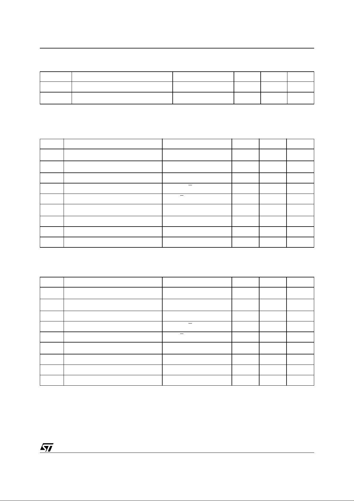
Table 1. Signal Names
A0-A16 Address Inputs
DQ0-DQ7 Data Inputs / Outputs
PFD
PFD
≤ 4.5V
≤ 3.0V
M48T128Y
M48T128V
32
1
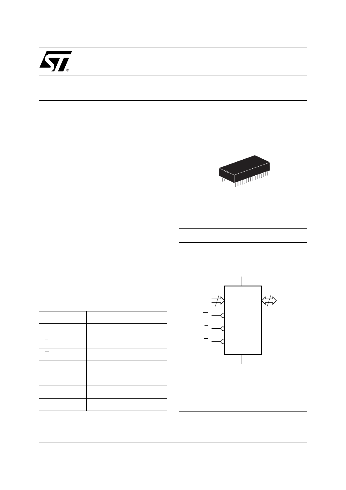
PMDIP32 (PM)
Module
Figure 1. Logic Diagram
V
CC
17
A0-A16 DQ0-DQ7
W
E
M48T128Y
M48T128V
8
E
G
W
V
CC
V
SS
NC Not Connected Internally
Chip Enable Input
Output Enable Input
Write Enable Input
Supply Voltage
Ground
G
V
SS
AI02244
1/14March 2000
Page 2
M48T128Y, M48T128V
Table 2. Absolute Maximum Ratings
Symbol Parameter Value Unit
T
A
T
STG
V
IO
V
CC
I
O
P
D
Note: 1. Stresses greater than those listed under "Absolute Maximum Ratings" may cause permanent damage to the device. This is a stress
2. Soldering temperature not to exceed 260°C for 10 seconds (total thermal budget not to exceed 150°C for longer than 30 seconds).
CAUTION: Negative undershoo ts bel ow –0.3V ar e not allowed on any pi n while in the B attery Back-up mode.
Ambient Operating Temperature 0 to 70 °C
Storage Temperature (VCC Off, Oscillator Off)
Input or Output Voltages
Supply Voltage
Output Current 20 mA
Power Dissipation 1 W
rating only and functi onal opera tion of the dev i ce at these or any other conditions above thos e i ndi cated in the operational section
of this spec ification is not im plied. Exposure t o the abso lute max imum rat ing cond itions for extende d period s of tim e may affe ct
reliability.
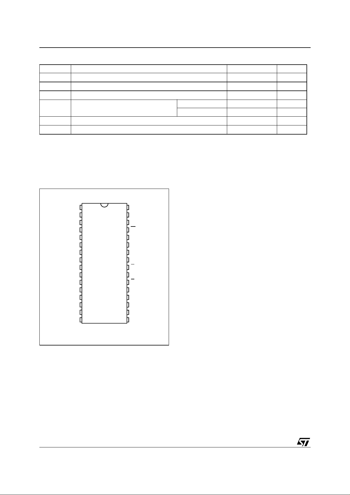
Figure 2. DIP C on ne ctions
(1)
–40 to 70 °C
–0.3 to V
M48T128Y –0.3 to 7.0 V
M48T128V –0.3 to 4.6 V
CC
+0.3
V
It also provides the non-volatility of Flash without
any requirement for special write timing or limitations on the number of writes that can be per-
NC V
1
A16
2
3
A14
4
A12
5
A7
6
A6
7
A5
8
A4
A3
A2
A1
A0
DQ0
DQ2
SS
M48T128Y
M48T128V
9
10
11
12
13
14
15
16
32
31
30
29
28
27
26
25
24
23
22
21
20
19
18
17
AI02245
CC
A15
NC
W
A13
A8
A9
A11
G
A10
E
DQ7
DQ6
DQ5DQ1
DQ4
DQ3V
formed. The 32 pin 600 mil DIP Hybrid houses a
controller chip, SRAM, quartz crystal, and a long
life lithium button cell in a single package.
Figure 3 illustrates the static memory array and the
quartz controlled clock oscillator. The clock locations contain the year, month, date, day, hour,
minute, and second in 24 ho ur BCD format. Corrections for 28, 29 (leap year), 30, and 31 day
months are made automatically. Byte 1FFF8 h is
the clock control register. This byte controls user
access to the clock information and also stores the
clock calibration setting. The seven clock bytes
(1FFFFh - 1FFF8h) are not the actual clock
counters, they are m emo ry locations cons isting of
BiPORT™ read/write memory cells within the static RAM array. The M48T128Y/V includes a clock
control circuit which updates the clock bytes with
current information once per second. The information can be accessed by the user in the same manner as any other location in the static memory
array. The M48T128Y/V also has its own PowerFail Detect circuit. This control circuitry constantly
monitors the supply voltage for an out of tolerance
DESCRIPTION
The M48T128Y/V TIMEKEEPER RAM is a 128Kb
x 8 non-volatile static RAM and real time clock.
The special DIP package provides a fully integrated battery back-up memory and real time clock so-
condition. When V
write pro te c ts the TIMEKEEPER register data an d
external SRAM, providing data security in the
midst of unpredictable system operation. As V
falls, the control circuitry automatically switches to
the battery, maintaining data and clock operation
until valid power is restored.
is out of t olerance, the ci rcuit
CC
CC
lution. The M48T128Y/V directly replaces industry
standard 128Kb x 8 SRAM.
2/14
Page 3
M48T128Y, M48T128V
≤ V
V
or
PFD
SO
CC
(1)
(min)
(2)
(2)
E G W DQ0-DQ7 Power
V
IH
V
IL
V
IL
V
IL
X X X High Z CMOS Standby
X X X High Z Battery Back-up Mode
Table 3. Operating Modes
Mode
Deselect
Write
Read
Read
Deselect
Deselect
Note: 1. X = VIH or VIL; VSO = Battery Back-up Swit ch ov er Volta ge.
2. See T able 7 for details.
4.5V to 5.5V
3.0V to 3.6V
V
to V
SO
READ MODE
The M48T128Y/V is in the Read Mode whenever
W
(Write Enable) is high and E (Chip Enable) is
low. The unique address specified by the 17 A ddress Inputs defines which one of the 131,072
bytes of data is to be accessed.
Valid data will be available at the Data I/O pins
within t
address input signal is stable, providing the E
G
access times are also satisfied. If the E and G
(Address Access Time) after the la st
AVQV
and
access tim es are not me t, valid da ta w ill be available after the latter of the Chip Enable Access
Times (t
(t
). The state of the eight three-state Data I/O
GLQV
signals is controlled by E
activated before t
to an indeterminate state until t
dress Inputs are changed while E
active, output data will remain valid for t
) or Output Enable Access Time
ELQV
and G. If the outputs are
, the data lines will be driven
AVQV
AVQV
. If the Ad-
and G remain
AXQX
(Output Data Hold Time) but will go indeterminate until
the next Addres s Acce ss.
X X High Z Standby
X
V
IL
V
IH
V
IL
V
IH
V
IH
D
IN
D
OUT
High Z Active
Active
Active
Table 4. AC Measurement Conditions
Input Rise and Fall Times ≤ 5ns
Input Pulse Voltages 0 to 3V
Input and Output Timing Ref. Voltages 1.5V
Note that Output Hi-Z is defined as the point where data is no longer
driven.
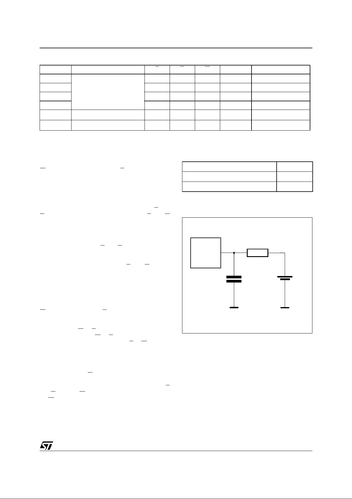
Figure 3. AC Testing Load Circuit
DEVICE
UNDER
TEST
650Ω
CL = 100pF
or 50pF
(2)
1.75V
(1)
WRITE MODE
The M48T128Y/V is in the Wri te Mode whenever
(Write Enable) and E (Chip Enable) are low
W
state after the address inputs are stable. The start
of a write is referenced from the latter occurring
falling edge of W
earlier rising edge of W
be held valid throughout the cycle. E
turn high for a minimum of t
or t
from Write Enable prior to the initiation of
WHAX
or E. A write is terminated by the
or E. The addresses must
or W must r e-
from Chip Enable
EHAX
another read or write cycle. Data-in must be valid
prior to the end of write and remain valid for
t
DVWH
t
afterward. G should be kept high during
WHDX
write cycles to avoid bus c ontention; although, if
the output bus has been activated by a low on E
and G a low on W will disable the outputs t
ter W
falls .
WLQZ
af-
CL includes JIG capacitance
Note: 1. 50pF for M48T128V (3.3V).
2. Exc l udi ng open dr ai n output pins.
AI03630
DATA RETENTION MODE
With valid V
applied, the M48T128Y/V operates
CC
as a conventional BYTEWIDE™ static RAM.
Should the supply voltage decay, the RAM will automatically deselect, write protecting itself when
V
falls between V
CC
(max), V
PFD
(min) win-
PFD
dow. All outputs become high impedance an d all
inputs are treated as "don't care".
3/14
Page 4
M48T128Y, M48T128V
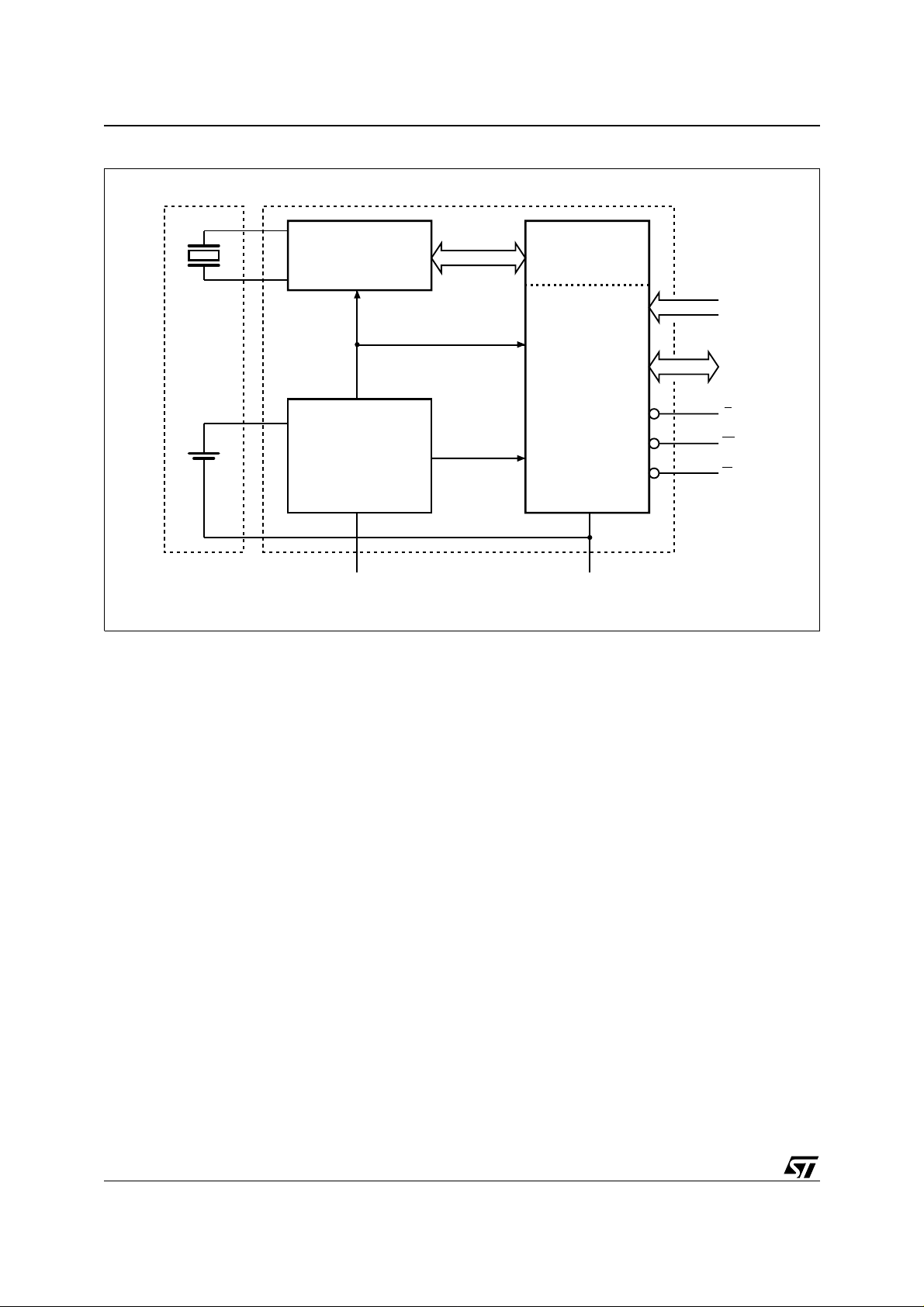
Figure 4. Block Diagram
OSCILLATOR AND
CLOCK CHAIN
32,768 Hz
CRYSTAL
POWER
LITHIUM
CELL
VOLTAGE SENSE
AND
SWITCHING
CIRCUITRY
V
CC
Note: A power failure during a write cycle may corrupt data at the current addressed location, but
does not jeopardize the rest of the RAM’s content.
At voltage s below V
in a write protected state, provided the V
time is not less than t
spond to transient noise s pi kes on V
(min), the memory will be
PFD
. The M48T128Y/V may re-
F
that cr os s
CC
CC
fall
into the deselect window during the time the device is sampling V
power supply lines is recomm ended. When V
. Therefore, decoupling of the
CC
CC
drops below VSO, the control circuit switches power to the internal battery, preserving data and powering the clock. The internal energy source will
maintain data in the M48T128Y/V for an accumulated period of at least 10 years at room tem perature. As system power rises above V
SO
, the
battery is disconnected, and the power supply is
switched to external V
t
after VCC reaches V
REC
. Deselect continues for
CC
(max).
PFD
8 x 8
TIMEKEEPER
REGISTERS
A0-A16
DQ0-DQ7
E
W
G
AI01804
V
PFD
131,064 x 8
SRAM ARRAY
V
SS
CLOCK OPERATIONS
Reading the Clock
Updates to the TIMEKEEPER registers should be
halted before clock data is read to prevent reading
data in transition. Because the BiPORT TIMEKEEPER cel ls in th e RAM array a re o n ly data re g isters, and not the actual clock counters, updating
the registers can be halted without disturbing the
clock itself. Updating is halted when a ’1’ is written
to the READ bit, D6 in the Control Register
(1FFF8h). As long as a ’1’ remains in that position,
updating is halted. After a halt is issued, the registers reflect the count; that is, the day, date, and
time that were current at the moment the halt command was issued. All of the TIMEKEEPER registers are updated simultaneously. A halt will not
interrupt an update in progress. Updating occurs 1
second after the READ bit is reset to a ’0’.
4/14
Page 5
M48T128Y, M48T128V
Table 5. Capacitance
(T
= 25 °C, f = MHz)
A
(1)
Symbol Parameter Test Condition Min Max Unit
C
IN
C
IO
Note: 1. Effective capacitance meas ured with po wer suppl y at 5V.
2. Outputs deselected.
Input Capacitance
(2)
Input / Output Capacitance
V
V
OUT
IN
= 0V
= 0V
20 pF
20 pF
Table 6A. DC Characteristics
= 0 to 70 °C; VCC = 4.5V to 5.5V)
(T
A
Symbol Parameter Test Condition Min Max Unit
(1)
I
LI
I
LO
I
I
V
V
V
Note: 1. Outputs deselected.
Input Leakage Current
(1)
Output Leakage Current
I
Supply Current Outputs open 95 mA
CC
Supply Current (Standby) TTL
CC1
Supply Current (Standby) CMOS
CC2
Input Low Voltage –0.3 0.8 V
V
IL
Input High Voltage 2.2
IH
Output Low Voltage
OL
Output High Voltage
OH
0V ≤ V
IN
0V ≤ V
OUT
E
= V
E
= VCC –0.2V
I
= 2.1mA
OL
I
= –1mA
OH
≤ V
≤ V
IH
CC
CC
±2 µA
±2 µA
8mA
4mA
V
+ 0.3
CC
0.4 V
2.4 V
V
Table 6B. DC Characteristics
= 0 to 70 °C; VCC = 3.0V to 3.6V)
(T
A
Symbol Parameter Test Condition Min Max Unit
(1)
Input Leakage Current
I
LI
(1)
Output Leakage Current
I
LO
I
I
I
V
V
V
Note: 1. Outputs deselected.
Supply Current Outputs open 50 mA
CC
Supply Current (Standby) TTL
CC1
Supply Current (Standby) CMOS
CC2
Input Low Voltage –0.3 0.4 V
V
IL
Input High Voltage 2.2
IH
Output Low Voltage
OL
Output High Voltage
OH
0V ≤ V
IN
0V ≤ V
OUT
E
= V
E
= VCC –0.2V
I
= 2.1mA
OL
I
= –1mA
OH
≤ V
≤ V
IH
CC
CC
±2 µA
±2 µA
4mA
3mA
V
+ 0.3
CC
0.4 V
2.2 V
V
5/14
Page 6

M48T128Y, M48T128V
Figure 5. Power Down/Up Mode AC Waveforms
V
CC
V
(max)
PFD
V
(min)
PFD
VSS
tF
tFB
INPUTS
OUTPUTS
VALID VALID
Table 7. Power Down/Up Trip Points DC Characteristics
tRB
DON'T CARE
HIGH-Z
(1)
tR
RECOGNIZEDRECOGNIZED
AI03612
(TA = 0 to 70 °C)
Symbol Parameter Min Typ Max Unit
V
PFD
V
SO
t
DR
Note: 1. All voltages referenced to VSS.
2. At 25°C.
Power-fail Deselect Voltage
Battery Back-up Switchover Voltage
(2)
Expected Data Retention Time 10 YEARS
M48T128Y 4.1 4.35 4.5 V
M48T128V 2.7 2.9 3.0 V
M48T128Y 3.0 V
V
M48T128V
PFD
–100mV
V
Table 8. Power Down/Up AC Characteristics
= 0 to 70 °C)
(T
A
Symbol Parameter Min Max Unit
(1)
t
F
t
FB
t
R
t
RB
t
REC
Note: 1. V
2. V
6/14
V
(max) to V
PFD
(2)
V
(min) to VSS VCC Fall Time
PFD
V
(min) to V
PFD
VSS to V
V
(max) t o V
PFD
(min).
V
PFD
(min) to VSS fall time of less than tFB may cause corruption of RAM data.
PFD
PFD
(max) to Inputs Recognized
PFD
(min) fall time of less than tF may re sul t in de sel ect io n/ wri te pr ot ec tio n n ot oc cu rr in g unt il 50µs af te r VCC passes
PFD
(min) VCC Fall Time
PFD
(max) VCC Rise Time
PFD
(min) VCC Rise Time
300 µs
10 µs
0µs
1µs
40 200 ms
Page 7

Table 9. Read Mode AC Characteristics
(T
= 0 to 70 °C)
A
M48T128Y, M48T128V
M48T128Y M48T128V
Symbol Parameter
Min Max Min Max
t
AVAV
t
AVQV
t
ELQV
t
GLQV
t
ELQX
t
GLQX
t
EHQZ
t
GHQZ
t
AXQX
Note: 1. CL = 100pF or 50pF (See Figu re 3).
2. C
Read Cycle Time 70 85 ns
(1)
Address Valid to Output Valid 70 85 ns
(1)
Chip Enable Low to Output Valid 70 85 ns
(1)
Output Enable Low to Output Valid 40 55 ns
(2)
Chip Enable Low to Output Transition 5 5 ns
(2)
Output Enable Low to Output Transition 5 5 ns
(2)
Chip Enable High to Output Hi-Z 25 30 ns
(2)
Output Enable High to Output Hi-Z 25 30 ns
(1)
Address Transition to Output Transition 10 5 ns
= 5pF.
L
Figure 6. Address Controlled, Read Mode AC Waveforms
Unit-70 -85
A0-A16
DQ0-DQ7
tAXQX
DATA VALID
tAVAV
VALID
tAVQV
DATA VALID
AI02324
7/14
Page 8
M48T128Y, M48T128V
Table 10. Write Mode AC Characteristics
(T
= 0 to 70 °C)
A
M48T128Y M48T128V
Symbol Parameter
t
AVAV
t
AVWL
t
AVEL
t
WLWH
t
ELEH
t
WHAX
t
EHAX
t
DVWH
t
DVEH
t
WHDX
t
EHDX
t
WLQZ
t
AVWH
t
AVEH
t
WHQX
Note: 1. CL = 5pF.
2. If E
Write Cycle Time 70 85 ns
Address Valid to Write Enable Low 0 0 ns
Address Valid to Chip Enable Low 0 0 ns
Write Enable Pulse Width 50 60 ns
Chip Enable Low to Chip Enable High 55 65 ns
Write Enable High to Address Transition 5 5 ns
Chip Enable High to Address Transition 10 15 ns
Input Valid to Write Enable High 30 35 ns
Input Valid to Chip Enable High 30 35 ns
Write Enable High to Input Transition 5 5 ns
Chip Enable High to Input Transition 10 15 ns
(1, 2)
Write Enable Low to Output Hi-Z 25 30 ns
Address Valid to Write Enable High 60 70 ns
Address Valid to Chip Enable High 60 70 ns
(1, 2)
Write Enable High to Output Transition 5 5 ns
goes low simultaneously with W going low, the ou tputs remain in the high im pedance st ate.
Unit-70 -85
Min Max Min Ma x
Setting the Clock
Bit D7 of the Control Register (1FFF8h) is the
WRITE bit. Setting the WR ITE bit to a '1', like the
READ bit, halts update s to the TIMEKEEPER r e g isters. The user can then loa d them with the correct day, date, and time data in 24 hour BCD
format (see Table 11). Resetting the WRITE bit to
a '0' then transfers the values of all time reg isters
1FFFFh-1FFF9h to the actual TIMEKEEPER
counters and allows normal operation to re sume.
After the WRITE bit is reset, the next clock update
will occur one second later.
8/14
Stopping and Starting the Oscillator
The oscillator may be stopped at any time. If the
device is going to spend a significant amount of
time on the shelf, the oscillator can be turned off to
minimize current drain on the battery. The STOP
bit is located at Bit D7 within 1FFF9h. Setting it to
a '1' stops the oscillator. The M48T128Y/V is
shipped from STMicroelectronics with the STOP
bit set to a '1'. When reset to a '0', the M48T128Y/
V oscillator starts after one second.
Page 9

M48T128Y, M48T128V
Figure 7. Chip Enable or Output Enable Controlled, Read Mode AC Waveforms
tAVAV
A0-A16
tAVQV tAXQX
tELQV
E
tELQX
G
tGLQX
DQ0-DQ7
VALID
tGLQV
Figure 8. Write Enable Controlled, Write AC Waveforms
tEHQZ
tGHQZ
DATA OUT
AI01197
A0-A16
E
W
DQ0-DQ7
tAVEL
tAVWL
tWLQZ
tAVAV
VALID
tAVWH
tWLWH
tDVWH
tWHAX
tWHQX
tWHDX
DATA INPUT
AI02382
9/14
Page 10

M48T128Y, M48T128V
Figure 9. Chip Enable Controlled, Write AC Waveforms
tAVAV
A0-A16
tAVEH
tAVEL
E
tAVWL
W
DQ0-DQ7
CALIBRATING THE CLOCK
The M48T128Y/V is driven by a quartz controlled
oscillator with a nominal frequency of 32,768Hz.
The devices are factory calibrated at 25°C and
tested for accuracy. Clock accuracy will not exceed 35 ppm (parts per million) oscillator frequency error at 25°C, which equates to about ±1.53
minutes per month. When the Calibration circuit is
properly employed, accuracy improves to better
than +4 ppm at 25°C. The oscillation rate of crystals changes with temperature.
The M48T128Y/V design employs periodic
counter correction. The calibration c ircuit adds or
subtracts counts from the o scillator divider circuit
at the divide by 128 stage, as shown in Figure 10.
The number of times pulses which are blanked
(subtracted, negative calibration) or split (added,
positive calibration) depends upon the value loaded into the five Calibration bits found in the Control
Register. Adding counts speeds the clock up, subtracting counts slows the clock down. The Calibration bits occupy the five lower order bits (D4-D0) in
the Control Register 1FFF8h. These bits can be
set to represent any value between 0 and 31 in binary form. Bit D5 is a Sign bit; '1' indicates positive
calibration, '0' indicates negative calibration. C alibration occurs within a 64 minute cycle. The first
62 minutes in the cycle may, once per minute,
have one second either shortened by 128 or
lengthened by 256 oscillator cycles. If a binary '1'
is loaded into the register, only the first 2 minutes
VALID
tELEH
DATA INPUT
tDVWH
tEHAX
tWHDX
AI02383
in the 64 minute cycle will be modified; if a binary
6 is loaded, the first 12 will be affected, and so on.
Therefore, each cal ibration step has the effect of
adding 512 or subtracting 256 oscillator cycles for
every 125, 829, 120 act ual o scillat or cycles, t hat i s
+4.068 or –2.034 ppm of adjustment per calibration step in the cal ibration registe r. Ass um ing that
the oscillator is running at exactly 32,768Hz, each
of the 31 increments in the Calibration byte would
represent +10.7 or –5.35 seconds per month
which corresponds to a total range of +5.5 or –2.75
minutes per month. Figure 10 illustrate s a TIMEKEEPER calibration waveform. One method is
available for ascertaining how much calibration a
given M48T128Y/V may require. This involves setting the clock, letting it run for a month and comparing it to a known accurate reference and
recording deviation over a fixed period of time.
Calibration values, including the number of seconds lost or gained in a given period, can be found
in STMicroelectronics Application Note: TIMEKEEPER CALI BRATION. T his all ows the des igner
to give the end user the ability to calibrate the
clock as the environment requires, even if the f inal
product is packaged in a non-user serviceable enclosure. The designer could provide a simple utility
that accesses the Calibration byte. For example, a
deviation of 21 seconds slow over a period of 30
days would indicate a –8 ppm oscillator frequency
error, requiring a +2(WR100010) to be loaded into
the Calibration Byte for correction.
10/14
Page 11

M48T128Y, M48T128V
Table 11. Register Map
Address
Data
D7 D6 D5 D4 D3 D2 D1 D0
1FFFFh 10 Years Year Year 00-99
1FFFEh 0 0 0 10 M. Month Month 01-12
1FFFDh 0 0 10 Date Date Date 01-31
1FFFCh 0 0 0 0 0 Day Day 01-07
1FFFBh 0 0 10 Hours Hours Hour 00-23
1FFFAh 0 10 Minutes Minutes Minutes 00-59
1FFF9h ST 10 Seconds Seconds Secon ds 00-59
1FFF8h W R S Calibration Control
Function/Rang e
BCD Format
Keys: S = SIGN Bit
R = READ Bit
W = WRITE Bit
ST = STOP Bit
Figure 10. Cal ib rat i on Waveform
NORMAL
POSITIVE
CALIBRATION
NEGATIVE
CALIBRATION
POWER SUPPLY DECOUPLING
and UNDERSHOOT PROTECTION
Note: I
transients, including those produced by
CC
output switching, can produce voltage fluctuations, resulting in spikes on the V
bus. These
CC
transients can be reduced if capacitors are used to
store energy, which stabilizes the V
bus. The
CC
energy stored in the bypass c apacitors will be released as low going spikes are generated or energy will be absorbed when overshoots occur. A
ceramic bypass capacitor value of 0.1µF is recommended in order to provide the needed filtering. In
0 = Must be set to zero
Z = ’0’ and ar e Read only
Y = ’1’ or ’0’
AI00594B
addition to transients that are caused by normal
SRAM operation, power cycling can generate negative voltage spikes on V
below V
by as much as one volt. These negative
SS
that drive it to values
CC
spikes can cause data corruption in the SRAM
while in battery backup mode. To protect from
these voltage spikes, ST recommends connecting
a schottky diode from V
nected to V
, anode to VSS). (Schottky diode
CC
to VSS (cathode con-
CC
1N5817 is recommended for through hole and
MBRS120T3 is recommended for surface mount).
11/14
Page 12

M48T128Y, M48T128V
Table 12. Ordering Information Scheme
Example: M48T128Y -70 PM 1
Device Type
M48T
Supply Voltage and Write Protect Voltage
Y = V
V = V
Speed
-70 = 70ns
-85 = 85ns
Package
PM = PMDIP32
Temperature Range
1 = 0 to 70 °C
= 4.5V to 5.5V; V
CC
= 3.0V to 3.6V; V
CC
= 4.1V to 4.5V
PFD
= 2.7V to 3.0V
PFD
For a list of available options (Speed, Pac kage, etc...) or for furthe r information on any aspect of this device, please contact the ST Sales Office nearest to you.
Table 13. Revision History
Date Revision Details
June 1998 First Issue
01/31/00 Calibrating The Clock Paragraph changed
03/30/00 Storage Temperature changed (Table 2)
12/14
Page 13

M48T128Y, M48T128V
Table 14. PMDIP32 - 32 pin Plastic Module DIP, Package Mechanical Data
Symbol
Typ Min Ma x Typ Min Max
A 9.27 9.52 0.365 0.375
A1 0.38 – 0. 015 –
B 0.43 0.59 0.017 0.023
C 0.20 0.3 3 0.008 0.013
D 42.42 43.18 1.670 1.700
E 18.03 18.80 0.710 0 .740
e1 2.29 2.79 0. 090 0.110
e3 34.29 41.91 1.350 1 .650
eA 14.99 16.0 0 0.590 0.630
L 3.05 3.81 0. 120 0.150
S 1.91 2.79 0.075 0.110
N32 32
mm inches
Figure 11. PMDIP32 - 32 pin Plastic Module DIP, Package Outline
A1AL
S
Be1
e3
D
N
E
1
Drawing is not to scale.
C
eA
PMDIP
13/14
Page 14

M48T128Y, M48T128V
Information furnished is believed to be accurate and reliable. However, STMicroelectronics assumes no responsibility for the consequences
of use of such information nor for any infringement of patents or other rights of third parties which may result from its use. No license is granted
by implic ation or o therwise under any patent or patent rights of STMicroelectronics. Specifications menti oned in thi s publicat i on are subject
to change without notice. This publication supersedes and replaces all information previously supplied. STMicroelectronics products a re not
authorized for use as c ri t i cal components in life support dev i ces or systems wi thout exp ress written approval of STMicroel ectronics.
The ST log o i s registered tradem ark of STMicroelectronics
2000 STMicroel e ctronics - All Ri ghts Reserved
All other names are the property of their resp ective owners.
Australi a - Brazil - C hi na - Finland - F rance - Germany - Hong Kong - In di a - Italy - Jap an - M alaysia - M al ta - Morocco -
Singapor e - Spain - Sweden - Switz erl and - Unit ed Kingdom - U.S.A.
STMicroelect ro n ics GRO UP OF COMPANI ES
http://www.st.com
14/14
 Loading...