

Page 1
LZ2346
Twopower
LZ2346
DESCRIPTION
LZ2346 is 1 /3-type (6.0 mm) solid-state image
sensor that consists of PN phote-diodes and
CCDS (charge-coupled devices) driven by only
positive voltages. Having approximately 220000
pixels (horizontal 384 X vertical 582), the sensor
provides a stable B/W image.
FEATURES
●
Number of pixels : 362 (H) X 582 (V)
Pixel pitch : 13.6
Number of optical black pixels
●
Low fixed pattern noise and lag
●
No sticking and no image distortion
●
Blooming suppression structure
●
Built-in output amplifier
●
Variable electronic shutter (1/50 to 1/10 000 s)
●
Compatible with
●
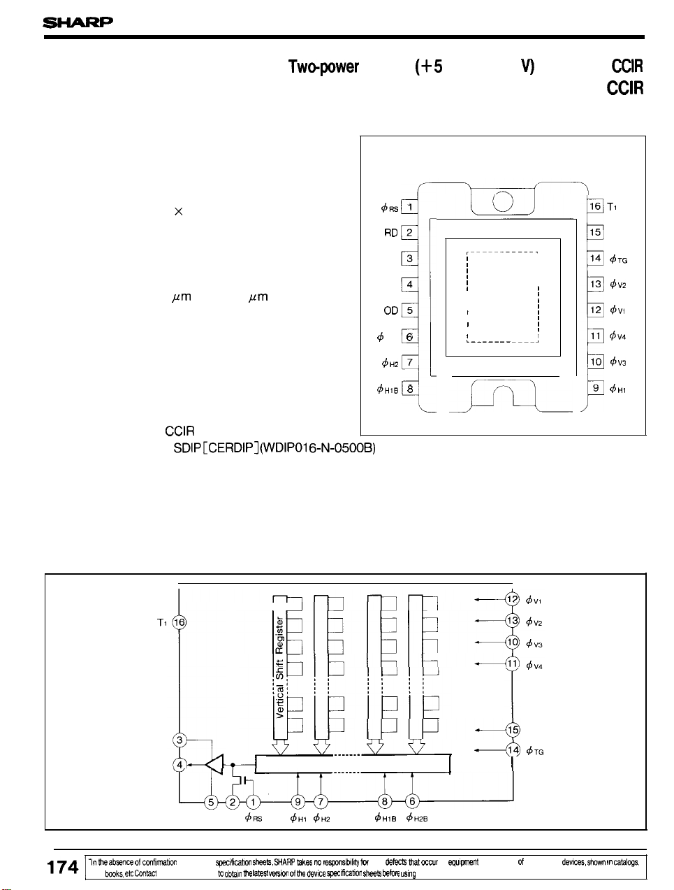
Package : 16-pin
Mm
(H) x 6.3 Km (V)
: Horizontal; front 2 and rear 20
CCIR
standard
SDIPICERDIP](WDIPO1 6-N-0500B)
1/3 type B/W CCD Area Sensor for
supply
(+5
V and +12 V) operation
PIN CONNECTIONS
16-PIN
SDIP
~m 1
RD 2
,—— ———. —— —-— .
GND 3
0s 4
OD 5
4
H2 B 6
dH2 7
dHIB 8
I
I
I
1
I
!
I
I
,
.—. ——— —— ..__ :
i
CCIR
CCIR
TOP VIEW
16 TI
15 OFD
14
4TG
I
I
I
1
I
I
1
,
13 4V2
12
4V1
11 4V4
10 4V3
9 tiH1
!
—
BLOCK DIAGRAM
GND
0s
“IO
tie
1741
abwnca of confimtlm
data Wks,
etc Untact
TI
by device ~!ticatron
SHARP
In
order to
II
t
OD RD
4175
shseb, WAR? tikaa rM msib!lm ti
obb+n me Iataat WM oi M deviw ~Ifimtion &b teti u~ng
Horizontal Shift Register
4H1
4.2
6H16 6H2B
any
dafecta Mat wcur
4
in
qu!mnt
any SHARPS device”
using any oi SHARPS
OFD
4TG
dewcea, shm !n cshlcgs,
Page 2
PIN DESCRIPTION
SYMBOL
RD
OD
I
0s
!
dRs
I dVi, $V2rdV3, dV4
4HI,4H2,4H16,4H2B
d TG
I
OFD
TI
GND
PIN NAME
Reset transistor drain
Output transistor drain
I
Video
OUtDUt
I
Reset transistor gate clock
I
Vertical shift register gate clock
Horizontal shift register gate clock
Transfer gate clock
I
Overflow drain
Test terminal
Ground
LZ2346
ABSOLUTE MAXIMUM RATINGS
PARAMETER
OutDut
transistor drain
Reset transistor drain voltage
Test terminal, TI
Reset gate clock voltage
Vertical shift register clock voltage
Horizontal shift register clock voltage
Transfer gate clock voltage
Overflow drain voltage
Storage temperature
ODeratina
ambient temperature
VOltage
SYMBOL
VOD
vRD
VTI
vdRs
Vdv
V+t.
V+TG
vOFD
Tstg
Topr
RATING
+15
Oto
Oto +15
Oto +15
–0.3 to +15
–0.3 to
+15
–0.3 to +15
–0,3 to +15
O to
+27
–40 to
+85
–20 to +70
(Ta
=25°C)
UNIT
v
v
v
v
v
v
v
v
“c
‘c
175
Page 3
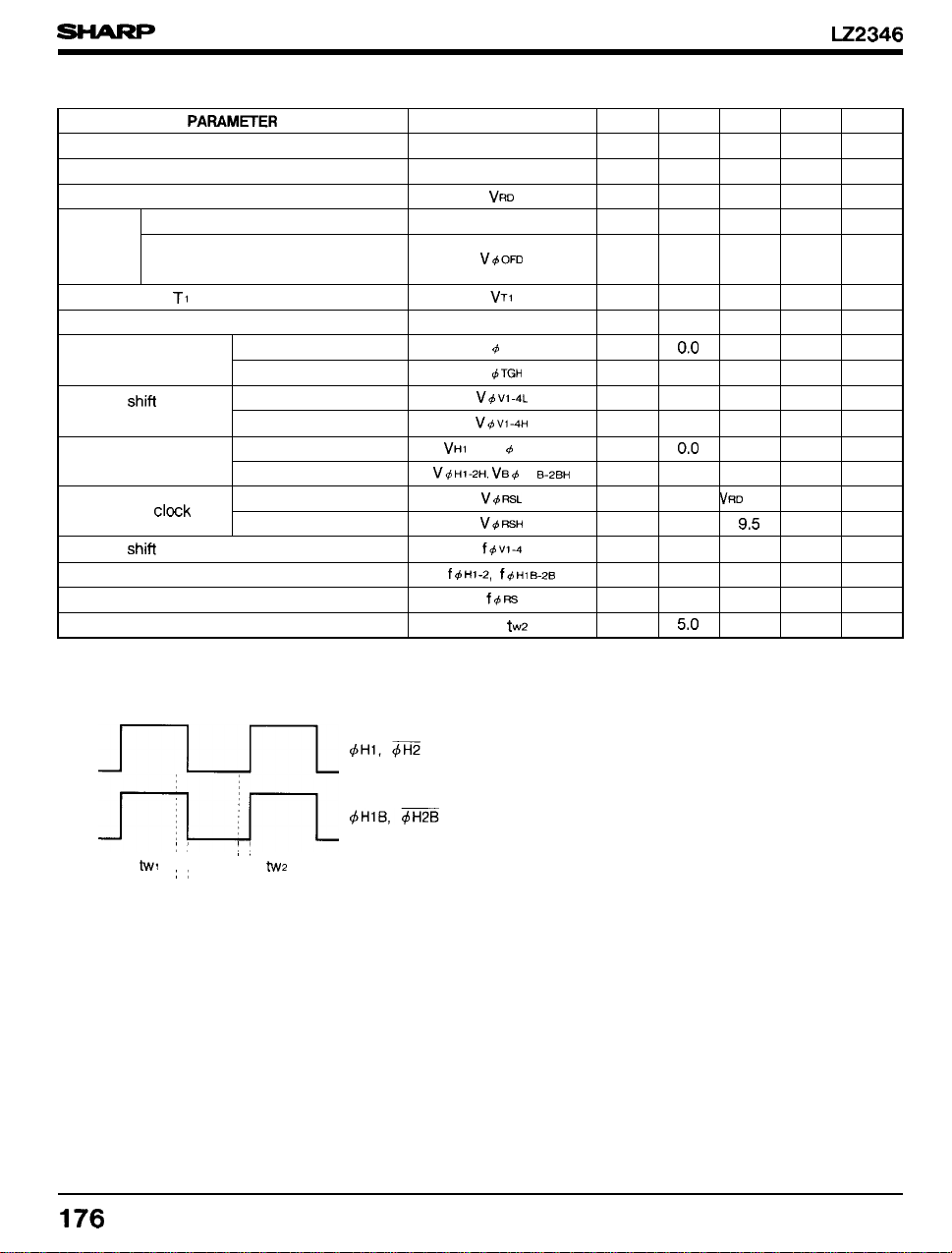
RECOMMENDED OPERATING CONDITIONS
PARAM~ER
Operating ambient temperature
Output transistor drain voltage
Reset transistor drain voltage
Overflow
drain
voltage
Test terminal, T!
Ground voltage
Transfer gate clock
Vertical
register clock
Horizontal shift
register clock
Reset gate
Vertical
Horizontal shift register clock frequency
Reset gate clock frequency
Horizontal shift register clock phase
When DC is applied
When pulse is applied
p-p level
LOW level
HIGH level
shiti
LOW level
HIGH level
LOW level
HIGH level
level
clcck
shif-t register clock frequency
LOW
HIGH
level
VH! -2L, V 4 HI B-2BL – 0.05
VdHI-ZH, VBd HI
SYMBOL
MIN.
Topr 25.0
Voo
VRD
V
OFD
V60m
VT1
GND
v
$
VdV1-4L
V4VI-4H
fdH1-2,
twl ,
TGL
v
dTGH
V4RSL
VdRSH
fdvl-4
f#HIB-2B
f$m
B-ZBH
twz
– 0.05 0.0 0.05
–
V
RD – 6.0
TYP.
12,0 12.5
3.0
MAX.
14.0
Voo
12,0 v
12,0 12.5 14.0
Voo
0.0
12.0
4.7
12.5 14,0
0.05
4.7
0.0 0,05
5.0 6.0
0,0
5.0
0.0
15.63
6,75 MHz
6.75 MHz
0.0
5,0
0.05
6.0
VHD
-10.5 v
9,5
10.0
UNIT
‘c
v
v
v
v
v
v
v
v
v
v
v
v
kHz
ns
LZ2346
NOTE
1
2
3
NOTES :
1. When DC voltage is applied, shutter speed is 1 /50 seconds.
2. When pulse is applied, shutter spaed is less than 1/50 seconds.
3
~
“
~
twl
,, ,,
-
::
,,
-
twz
‘H’”
‘“l’”
176
Page 4

LZ2346
ELECTRICAL CHARACTERISTICS (Drive method : Field Accumulation)
(Ta = 2SC, Operating conditions : typical values for the recommended operating conditions, Color
temperature of light source :3200 K /
PARAMHER
Photo response non-uniformity
Saturation signal
Dark output voltage
Dark signal non-uniformity
Sensitivity
Smear ratio
Image lag
Blooming suppression ratio
trasistor
Output
output impedance
drain current
IR
cut-off filter (CM-500, 1
SYMBOL
PRNU
vast
Vdark
DSNU
R
SMR – 85 – 76
Al
ABL 1000
IOD
Ro
MIN.
450
140
mmt))
TYP. MAX.
5.0
1.5
200
2.5
400
15
15.0
5.0
1.0
5.0
UNIT NOTE
~/0
mV
mV
mV
mV
dB
%
mA
a
2
3
1, 4
1, 5
6
7
8
9
I
g
<
● The standard output voltage is defined as 150
average output voltage under uniform illumination.
● The standard exposure level is defined when the average
output voltage is 150
mV
under uniform illumination.
mV
by the
NOTES :
1
Ta :
+WC
The image area is divided mto 10X 10 segments. Tk
2
ment’s
voltage is the average output voltage of all the
pixels within the segment. PRNU is defined by (Vmax –
Vmin)/Vo,
the minimum values of each segment’s voltage respectively, when the average output voltage Vo is 150 mV.
The image area is divided into 10x
3
The saturation signal is defined as the minimum of each
segment’s voltage which is the average output voltage of
all the pixels within the segment, when the exposure level
is ~t as 10 times, compared to standard level.
4
The average output voltage under a
The image area is
5
defined by
where Vmax and Vmin are the maximum and
10 segments.
non-e-re @lticm.
(Vdmax
div!ded
into 10x 10 segments. OSNU is
–
Vdmin)
under the non-exposure con-
~-
dition where Vdmax and Vdmin are the maximum and
minimum values of each segment’s voltage, respective y,
that is the average output voltage over al
segment.
6.
The average output voltage when a 1 COO
attached with a 90% reflector is imaged by a lens of
f50 mm.
7,
The sensor is adjusted to position a V/l O square at the
center of image area
image area. SMR is defined by the ratio of the output
voltage detected during the vertical blanking
maximum of the pixel voltage in the V/l O square.
8,
The sensor is
ing to the standard condition preceding
dition. Al is defined by the ratio between the output voltage measured at the 1st field during the non-exposure
period and the standard output voltage.
9
The sensor is adjusted to position a V/l O square at the
center of image area. ABL is the ratio between the
Dsure at the standard condition and the exposure at a
mint where a
ex~d
blmming
Mere
V is the
at the
exmsure
is observed.
I
pixels in the
Iux
light source
vetilcal
length of the
level
ncm-exposure
pericxl
corresWnd-
M
F4,
to the
con-
ex-
177
Page 5

PIXEL STRUCTURE
LZ2346
SPECTRAL
100
80
w
>
:
40
K
OPTICAL BIACK
(2 PIXELS)
~
RESPONSE EXAMPLE
7
362 (H)
\
X 582
(v)
OPTICAL BLACK
/
(20 PIXELS)
178
20
0
400
1
6~
800
Ooil
1200
Page 6

TIMING DIAGRAM EXAMPLE
(Ist,
3rd FIELD)
623
HD
VD
A
uuu uuu u
4V1
d
V2 u
d V3
d
V4
dTG
0s
Kuuuu
n
J
n
n
~
582
WI
Juu
625 1
n
n
n
n n
nnJ
n
n
VERTICAL TRANSFER TIMING
5
n
nnn
n
n
I
u uHuuuuuIu
u u
u
n
u u
n
n
n n
u
n
n
uuu
n
n
n
n
uuu u
n
n
n
n
LZ2346
19
n n
n
n
u
u
u
u
n
n
n
n
n
n
n
n
u u
n
n n
n
n
n n
n
n
n
n
n
u
u
u
u
n
n
n
n n n n
r
u
u u
n
n
n
n
n n
357
!+++
2468
u
u I
n
n
I
II
u
(2nd. 4th
.,
HELD)
HD
VD
4V1
4
V2
d
V3
0s
dH1
dH2
d
RS
0s
311
n
J
1
u
nnn n
u uuu
u u uuuuu
~~
n
n
n
n
5:9 %+1
w
582
I
. . . . . . . . . . . . . ...362
u u u u
n n n
OB(20)
n
318
,
n n
n
[
n
n
uuI u u u u u
u~Ll
u
u
n
n
HORIZONTAL TRANSFER
J
nnnnn n
n
n
I
n
n
n
u
~
TIMING
06(2)
nnn
uuu u
n n
n
n
1..0UPUT(362)
331
u u u
246
+++
n
n
n
nnn
u
u uuu
u
u
n
n n n
n
. . . . . . . . . . . . . . . . . . . . . .
179
Page 7

READOUT TIMING
LZ2346
(1S, 3rd
(2nd,
FIELD)
180
Page 8

SYSTEM CONFIGURATION EXAMPLE
—
1
*
—
]
m
dso
I
*“
L
II
ll
181
 Loading...