

Page 1
In the absence of confirmation by device specification sheets, SHARP takes no responsibility for any defects that may occur in equipment using any SHARP devices shown in
catalogs, data books, etc. Contact SHARP in order to obtain the latest device specification sheets before using any SHARP device.
1
DESCRIPTION
The LZ21N3V/VS are 1/2-type (8.08 mm) solidstate image sensors that consist of PN photodiodes and CCDs (charge-coupled devices). With
approximately 2 140 000 pixels (1 704 horizontal x
1 255 vertical), the sensor provides a stable highresolution color image.
FEATURES
• Optical size : 8.08 mm (aspect ratio 4 : 3)
• Interline scan format
• Square pixel
• Number of effective pixels : 1 650 (H) x 1 250 (V)
• Number of optical black pixels
– Horizontal : 2 front and 52 rear
– Vertical : 3 front and 2 rear
• Number of dummy bits
– Horizontal : 28
– Vertical : 2
• Pixel pitch : 3.95 µm (H) x 3.95 µm (V)
• R, G, and B primary color mosaic filters
• Supports monitoring mode
• Low fixed-pattern noise and lag
• No burn-in and no image distortion
• Blooming suppression structure
• Built-in output amplifier
• Built-in overflow drain voltage circuit and reset
gate voltage circuit
• Variable electronic shutter
• Packages
– LZ21N3V : 20-pin half-pitch WDIP [Plastic]
(WDIP020-P-0500)
Row space : 12.20 mm
– LZ21N3VS : 20-pin half-pitch WSOP [Plastic]
(WSOP020-P-0525)
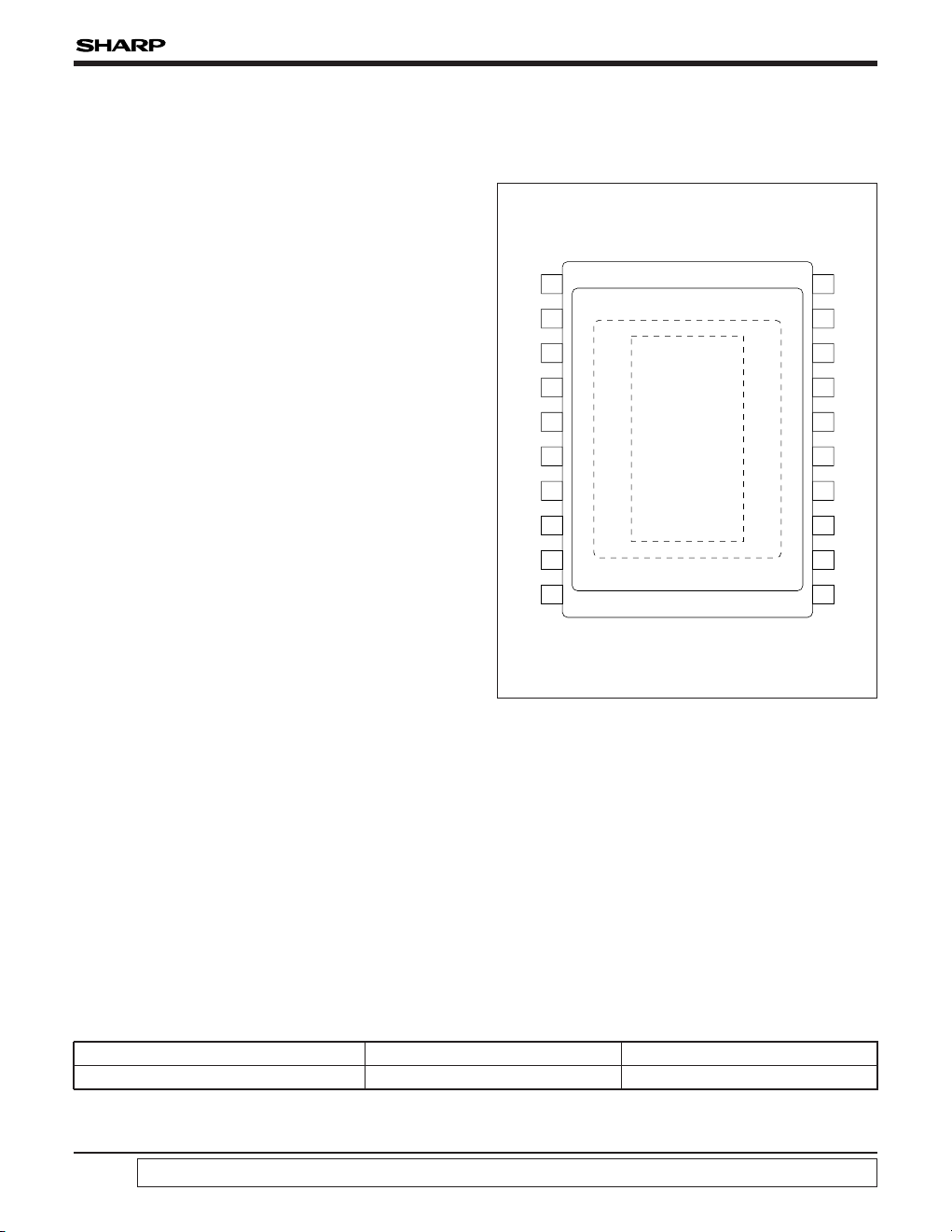
PIN CONNECTIONS
PRECAUTIONS
• The exit pupil position of lens should be 30 to 50
mm from the top surface of the CCD.
• Refer to "PRECAUTIONS FOR CCD AREA
SENSORS" for details.
LZ21N3V/VS
LZ21N3V/VS
1/2-type Interline Color CCD
Area Sensors with 2 140 k Pixels
1OD
2GND
3OFD
4PW
5Ø
RS
6NC1
7NC2
8ØH1
9NC3
10ØH2
20
19
18
17
16
15
14
OS
GND
NC
5
NC4
ØV1A
ØV1B
ØV2
13 ØV3A
12 ØV3B
11 ØV4
20-PIN HALF-PITCH WDIP
20-PIN HALF-PITCH WSOP
TOP VIEW
(WDIP020-P-0500)
(WSOP020-P-0525)
Package
LZ21N3V
20-pin half-pitch WDIP
COMPARISON TABLE
20-pin half-pitch WSOP
LZ21N3VS
Page 2

2
LZ21N3V/VS
PIN DESCRIPTION
SYMBOL PIN NAME
OD Output transistor drain
OS Output signals
ØRS Reset transistor clock
Ø
V1A, ØV1B, ØV2, ØV3A, ØV3B, ØV4 Vertical shift register clock
ØH1, ØH2 Horizontal shift register clock
PW P-well
GND Ground
NC1, NC2, NC3, NC4, NC
5
No connection
Overflow drainOFD
ABSOLUTE MAXIMUM RATINGS (TA = +25 ˚C)
PARAMETER SYMBOL RATING UNIT
Output transistor drain voltage V
OD 0 to +15 V
Reset gate clock voltage V
ØRS Internal output V
Vertical shift register clock voltage V
ØV VPW to +15 V
Horizontal shift register clock voltage VØH –0.3 to +12 V
Voltage difference between P-well and vertical clock V
PW-VØV –24 to 0 V
Storage temperature T
STG –40 to +85 ˚C
Ambient operating temperature T
OPR –20 to +70 ˚C
2
NOTE
NOTES :
1. Do not connect to DC voltage directly. When OFD is connected to GND, connect VOD to GND. Overflow drain clock is
applied below 22 Vp-p.
2. Do not connect to DC voltage directly. When Ø
RS is connected to GND, connect VOD to GND. Reset gate clock is
applied below 8 Vp-p.
3. When clock width is below 10 µs, and clock duty factor is below 0.1%, voltage difference between vertical clocks will be
below 22 V.
1VInternal outputVOFDOverflow drain voltage
3V0 to +15V
ØV-VØVVoltage difference between vertical clocks
Page 3

3
LZ21N3V/VS
RECOMMENDED OPERATING CONDITIONS
PARAMETER SYMBOL MIN. TYP. MAX. UNIT NOTE
Ambient operating temperature T
OPR 25.0 ˚C
Output transistor drain voltage V
OD 12.5 13.0 13.5 V
NOTES :
1. Use the circuit parameter indicated in "SYSTEM CONFIGURATION EXAMPLE", and do not connect to DC voltage directly.
2. V
PW is set below VØVL that is low level of vertical shift register clock, or is used with the same power supply that is connected
to V
L of V driver IC.
* To apply power, first connect GND and then turn on V
OD. After turning on VOD, turn on PW first and then turn on other powers
and pulses. Do not connect the device to or disconnect it from the plug socket while power is being applied.
1V20.919.518.6VØOFD
Overflow drain clock
P-well voltage VPW –8.0 VØVL V2
Ground GND 0.0 V
V–6.65–7.0–7.35
V
ØV1AL, VØV1BL, VØV2L
VØV3AL, VØV3BL, VØV4L
Vertical shift
register clock
LOW level
INTERMEDIATE level
HIGH level
V
ØV1AI, VØV1BI, VØV2I
VØV3AI, VØV3BI, VØV4I
VØV1AH, VØV1BH
VØV3AH, VØV3BH
12.5
0.0
13.0 13.5VV
LOW levelHorizontal shift
register clock
V
ØH1L, VØH2L –0.05 0.0 0.05 V
HIGH level V
ØH1H, VØH2H 4.5 4.8 5.5 V
1V5.54.84.5V
ØRSReset gate clock p-p level
Reset gate clock frequency f
ØRS 17.94 MHz
Horizontal shift register clock frequency f
ØH1, fØH2 17.94 MHz
Vertical shift register clock frequency
f
ØV1A, fØV1B, fØV2
fØV3A, fØV3B, fØV4
7.87 kHz
p-p level
Page 4

LZ21N3V/VS
4
CHARACTERISTICS (Drive method : 1/30 s frame accumulation)
(T
A = +25 ˚C, Operating conditions : The typical values specified in "
RECOMMENDED OPERATING CONDITIONS
".
Color temperature of light source : 3 200 K, IR cut-off filter (CM-500, 1 mmt) is used.)
PARAMETER SYMBOL MIN. TYP. MAX. UNIT NOTE
Standard output voltage V
O 150 mV 2
Photo response non-uniformity PRNU 10 % 3
Saturation output voltage V
SAT
450 530 mV 4
Dark output voltage V
DARK 0.5 3.0 mV 1, 6
Dark signal non-uniformity DSNU 0.5 2.0 mV 1, 7
Sensitivity (green channel) R 140 180 mV 8
Smear ratio SMR –89 –82 dB 9
Image lag AI 1.0 % 10
Blooming suppression ratio ABL 1 000 11
Output transistor drain current I
OD 4.0 8.0 mA
NOTES :
• Within the recommended operating conditions of VOD,
V
OFD of the internal output satisfies with ABL larger than
1 000 times exposure of the standard exposure conditions,
and V
SAT larger than 320 mV.
1. T
A = +60 ˚C
2. The average output voltage of G signal under uniform
illumination. The standard exposure conditions are
defined as when Vo is 150 mV.
3. The image area is divided into 10 x 10 segments under
the standard exposure conditions. Each segment's
voltage is the average output voltage of all pixels within
the segment. PRNU is defined by (Vmax – Vmin)/Vo,
where Vmax and Vmin are the maximum and minimum
values of each segment's voltage respectively.
4. The image area is divided into 10 x 10 segments. Each
segment's voltage is the average output voltage of all
pixels within the segment. V
SAT is the minimum
segment's voltage under 10 times exposure of the
standard exposure conditions. The operation of OFDC is
high. (for still image capturing)
5. The image area is divided into 10 x 10 segments. Each
segment's voltage is the average output voltage of all
pixels within the segment. V
SAT is the minimum
segment's voltage under 10 times exposure of the
standard exposure conditions. The operation of OFDC is
low.
6. The average output voltage under non-exposure
conditions.
7. The image area is divided into 10 x 10 segments under
non-exposure conditions. DSNU is defined by (Vdmax –
Vdmin), where Vdmax and Vdmin are the maximum and
minimum values of each segment's voltage respectively.
8. The average output voltage of G signal when a 1 000
lux light source with a 90% reflector is imaged by a lens
of F4, f50 mm.
9. The sensor is exposed only in the central area of V/10
square with a lens at F4, where V is the vertical image
size. SMR is defined by the ratio of the output voltage
detected during the vertical blanking period to the
maximum output voltage in the V/10 square.
10. The sensor is exposed at the exposure level
corresponding to the standard conditions. AI is defined
by the ratio of the output voltage measured at the 1st
field during the non-exposure period to the standard
output voltage.
11. The sensor is exposed only in the central area of V/10
square, where V is the vertical image size. ABL is
defined by the ratio of the exposure at the standard
conditions to the exposure at a point where blooming is
observed.
5mV400320
Page 5
LZ21N3V/VS
5
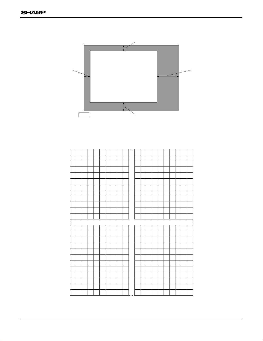
PIXEL STRUCTURE
1 650 (H) x 1 250 (V)
1 pin
OPTICAL BLACK
(2 PIXELS)
OPTICAL BLACK
(52 PIXELS)
OPTICAL BLACK
(3 PIXELS)
OPTICAL BLACK
(2 PIXELS)
COLOR FILTER ARRAY
(1, 1 250) (1 650, 1 250)
(1, 1)
(1 650, 1)
Ø
V3B
ØV1B
ØV3A
ØV1B
ØV3B
ØV1B
ØV3B
ØV1A
ØV3B
ØV1B
ØV3B
ØV1B
ØV3B
ØV1B
ØV3B
ØV1B
ØV3A
ØV1B
ØV3B
ØV1B
ØV3B
ØV1A
ØV3B
ØV1B
G
RGRGRGRGRG
BGBGBGBGB G
RGRGRGRGRG
BGBGBGBGB
G
RGRGRGRGRG
BGBGBGBGB G
RGRGRGRGRG
BGBGBGBGB
G
RGRGRGRGRG
BGBGBGBGB G
RGRGRGRGRG
BGBGBGBGB
G
RGRGRGRGRG
BGBGBGBGB G
RGRGRGRGRG
BGBGBGBGB
G
RGRGRGRGRG
BGBGBGBGB G
RGRGRGRGRG
BGBGBGBGB
G
RGRGRGRGRG
BGBGBGBGB G
RGRGRGRGRG
BGBGBGBGB
G
RGRGRGRGRG
BGBGBGBGB G
RGRGRGRGRG
BGBGBGBGB
G
RGRGRGRGRG
BGBGBGBGB G
RGRGRGRGRG
BGBGBGBGB
G
RGRGRGRGRG
BGBGBGBGB G
RGRGRGRGRG
BGBGBGBGB
G
RGRGRGRGRG
BGBGBGBGB G
RGRGRGRGRG
BGBGBGBGB
G
RGRGRGRGRG
BGBGBGBGB G
RGRGRGRGRG
BGBGBGBGB
G
RGRGRGRGRG
BGBGBGBGB G
RGRGRGRGRG
BGBGBGBGB
Pin arrangement
of the vertical
readout clock
Page 6
LZ21N3V/VS
6
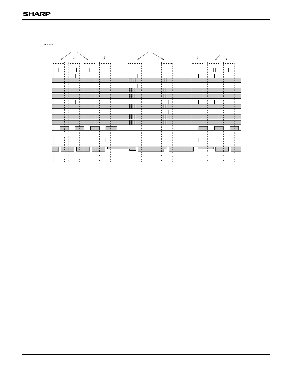
TIMING CHART
NOTES :
1. Do not use these signals immediately after field accumulation mode is transferred to frame
accumulation mode for still image capturing.
2. Do not use these signals immediately after frame accumulation mode is transferred to field
accumulation mode for monitoring image.
* Apply at least an OFD shutter pulse to OFD in each field accumulation mode.
ØV3A
ØV2
ØV1B
ØV1A
VD
TIMING CHART EXAMPLE
OS
OFDC
Ø
OFD
ØV4
ØV3B
263
525 1 1263
525
656 1 263 525 1
656
1
656
1
(at OFD shutter operation)
(Number of
vertical line)
Pulse diagram in more detail is shown in figures q to t after the next page.
Field accumulation mode Frame accumulation
mode at first
Frame accumulation mode Field accumulation
mode at first
Field accumulation
mode
qqwe rtqq'q'
Field accumulation mode Field accumulation
Not for use
(NOTE 1)
Not for use
(NOTE 2)
Frame accumulation mode
(3, 8, 13,..) (3, 8, 13,..) (3, 8, 13,..)
(1, 3,
...
, 1247, 1249) (2, 4,
...
, 1248, 1250)
mode (3, 8, 13,
..
)
Page 7

LZ21N3V/VS
7
ØV3A
ØV2
ØV3B
OS
Ø
V1B
ØV1A
HD
VD
Ø
OFD
OFDC
ØV4
q VERTICAL TRANSFER TIMING ¿FIELD ACCUMULATION MODE¡
257 258 259 260 261 262 263 264 265 266 267 268 269 270 271 272 273 274 275 276 277 278 279 280 281 282 283 284
OB1
RG GB RG GB
818313
RG GB RG GB
1238 1248
1233 1243
RG GB RG GB
1218 1228
1213 1223
GB RG GB
1198 1208
1203
Shutter speed
1/30 s
ØV3A
ØV2
ØV3B
OS
Ø
V1B
ØV1A
HD
VD
Ø
OFD
OFDC
Ø
V4
519 520 521 522 523 524 525 1 2 3 4 5 6 7 8 9 10 11 12 13 14 15 16 17 18 19 20 21
OB1
RG GB RG GB
818313
RG GB RG GB
1238 1248
1233 1243
RG GB RG GB
1218 1228
1213 1223
GB RG
RG GB
1198 1208
12031193
q' VERTICAL TRANSFER TIMING ¿FIELD ACCUMULATION MODE¡
Shutter speed
1/30 s
Page 8

LZ21N3V/VS
8
ØV3A
ØV2
ØV3B
OS
Ø
V1B
ØV1A
HD
VD
ØOFD
OFDC
Ø
V4
519 520 521 522 523 524 525 1 2 3 4 5 6 7 8 9 10 11 12 13 14 15 16 17 18 19 20 21
RG GB RG GB
1238 1248
1233 1243
RG GB RG GB
1218 1228
1213 1223
GB RGRG GB
1198 1208
12031193
Not for use
w VERTICAL TRANSFER TIMING ¿FRAME ACCUMULATION MODE AT FIRST¡
Shutter speed
1/15 s
ØOFD
ØV3A
OFDC
Ø
V4
ØV3B
ØV2
ØV1B
ØV1A
VD
HD
e VERTICAL TRANSFER TIMING ¿FRAME ACCUMULATION MODE¡
618 619 620 621 622 623 624
…
655 656 1 2 9 10 1211 13 1514 1716 1918 2120
OS
OB2 1 3 5
RG RG RG
Not for use
Charge swept transfer (1 368 stages)
…
…
* Do not use the frame signals immediately after accumulation mode is transferred to frame
accumulation mode.
* Do not use the frame signals immediately after field accumulation mode is transferred to frame
accumulation mode.
Page 9

LZ21N3V/VS
9
ØOFD
ØV3A
OFDC
Ø
V4
ØV3B
ØV2
ØV1B
ØV1A
VD
HD
r VERTICAL TRANSFER TIMING ¿FRAME ACCUMULATION MODE¡
638 639 640 641 642 643 644 645 646 656 1 2 9 10 1211 13 1514 1716 1918 2120
OS
OB1 OB3 2 4
GB GBRG RGRGRG RG
Not for use
Charge swept transfer (684 stages)
… …
OB1
1249
1243 1247
12451241
ØOFD
ØV3A
OFDC
ØV4
ØV3B
ØV2
ØV1B
ØV1A
VD
HD
t VERTICAL TRANSFER TIMING ¿FIELD ACCUMULATION MODE AT FIRST¡
640 641 642 643 644 656
…
6571234 98101211 13 1514 1716 1918 2120
OS
1244 OB2
1246
1248
1250
GBGB GB GB
Shutter speed
1/15 s
Page 10

LZ21N3V/VS
10
40.9 µs (732 bits)
58.8 µs (1 052 bits)
(120 bits)
(120 bits)
892
ØV3A
ØV4
ØV3B
ØV2
ØV1A
HD
92 212
172 292
52 252
132 332
2280, 1 228
292
252
332
212
2282280, 1
932
11721052
1012
732 852
972
6.7 µs
6.7 µs
Ø
V1B
READOUT TIMING ¿FIELD ACCUMULATION MODE¡
40.9 µs (732 bits)
58.8 µs (1 052 bits)
(120 bits)
(120 bits)
892
972
ØV3A
Ø
V3B
ØV4
ØV2
ØV1A
ØV1B
HD
92 212
172 292
52 252
132 332
228
292
252
332
212
2282280, 1
732 852
932
1012
6.7 µs
6.7 µs
READOUT TIMING ¿FRAME ACCUMULATION MODE¡e
r
892
1052 1172
92 212
172 292
52 252
132 332
228
932
1012
2280, 1
212
292
252
332
2282280, 1
2280, 1
ØV3A
ØV3B
ØV4
ØV2
ØV1A
ØV1B
HD
972
* Keep over 2.2 µs when vertical transfer clock pulse is overlapping.
* Keep over 2.2 µs when vertical transfer clock pulse is overlapping.
Page 11

LZ21N3V/VS
11
OS
Ø
RS
ØH2
ØH1
HD
OB (52)
HORIZONTAL TRANSFER TIMING ¿FIELD ACCUMULATION MODE¡-1
1 clk = 55.8 ns (= 1/17.9 MHz)
2280, 1
52 92 132 172 212 228 252 292 332
40 clk (= 2.2 µs)
Double transfer
OFD
Ø
V4
ØV2
ØV1A
ØV1B
ØV3A
ØV3B
ØV4
ØV2
ØV1A
ØV1B
ØV3A
ØV3B
Triple transfer
192 272
πππ
1650
Page 12

LZ21N3V/VS
12
OS
Ø
RS
ØH2
ØH1
HD
Ø
V4
ØV2
HORIZONTAL TRANSFER TIMING ¿FIELD ACCUMULATION MODE¡-2
1 clk = 55.8 ns (= 1/17.9 MHz)
332
ØV1A
ØV1B
ØV3A
ØV3B
372 412 452 492 532 572 600
Double transfer
OFD
ØV4
ØV2
ØV1A
ØV1B
ØV3A
ØV3B
Triple transfer
OUTPUT (1 650) 1
πππππππ
OB (2)
PRE SCAN (28)
Page 13

LZ21N3V/VS
13
OS
Ø
RS
ØH2
ØH1
HD
OB (52)
HORIZONTAL TRANSFER TIMING ¿FRAME ACCUMULATION MODE¡-1
1 clk = 55.8 ns (= 1/17.9 MHz)
2280, 1
..
1650
52 92 132 172 212 228 252 292 332
40 clk (= 2.2 µs)
Standard transfer
OFD
Ø
V4
ØV2
ØV1A
ØV1B
ØV3A
ØV3B
192 272
OS
Ø
RS
ØH2
ØH1
HD
HORIZONTAL TRANSFER TIMING ¿FRAME ACCUMULATION MODE¡-2
1 clk = 55.8 ns (= 1/17.9 MHz)
332
372 412 452 492 532 572 600
Standard transfer
OFD
Ø
V4
ØV2
ØV1A
ØV1B
ØV3A
ØV3B
OUTPUT (1 650) 1
ππππππππ
OB (2)
PRE SCAN (28)
Page 14

ØV1A
ØV1B
ØV4
ØV3A
ØV3B
ØV2
HD
CHARGE SWEPT TRANSFER TIMING ¿e¡
621H
• • • • •
11H 12H3H2H1H656H
• • • • •
655H623H622H 13H
1 228
2242
2 42 16212282
2 42 16212282
1234
• • • • • • •
136813671366
2262
22 62 142102
2262
22 62 142102
2242
CHARGE SWEPT TRANSFER TIMING ¿r¡
ØV1A
ØV1B
ØV4
ØV3A
ØV3B
ØV2
HD
645H
• • • • •
11H 12H3H2H1H656H
• • • • •
655H647H646H 13H
1 228
2242
2 42 16212282
2 42 16212282
12 34
• • • • • • •
684683682
2262
22 62 142102
2262
22 62 142102
2242
LZ21N3V/VS
14
* Keep over 1.1 µs when vertical transfer clock pulse of charge swept transfer is overlapping.
* Keep over 1.1 µs when vertical transfer clock pulse of charge swept transfer is overlapping.
Page 15

LZ21N3V/VS
15
100 k$33 k$
OD
PW
OFD
Ø
V2
ØV1B
ØV3A
ØV3B
ØV4
GND
NC1
NC2
ØH1
NC3
ØH2
OS
GND
NC
5
NC4
ØV1A
ØRS
V3B
V3A
V1B
V1A
VMa
VH
V4
V2
VL
VMb
POFD
NC
VH
ØH2
VH1BX
V3X
V2X
VH3BX
V4X
V1X
VH3AX
VH1AX
+VDD
OFDX
ØH1
ØRS
VL (VPW)
CCD
OUT
VOFDH
VH3BX
OFDX
V
2X
V1X
V3X
VDD
GND
V
4X
VH3AX
VH1BX
VH1AX
+
+
1234567812
242322212019181713
11
14
10
15
9
16
2345678
1918
1
201716151413
910
1211
LR36685 LZ21N3V
(*1)(*1)
VOD
OFDC
270
pF
100 $
1 M$
1 M$
5.6 k$
47 k$
0. 1 µF1.0 µF
0.01 µF
+
+
(*1) ØRS, OFD :
Use the circuit parameter indicated in
this circuit example, and do not connect
to DC voltage directly.
SYSTEM CONFIGURATION EXAMPLE
Page 16

PACKAGES FOR CCD AND CMOS DEVICES
16
,
,
,
,
,
,
,
,
,,,,,,,,,,,,,,,,,,,,,,,,,,,,,,,,,,,,,,,,,,,,,,,,,,,,,,,,,,,,,,,,,,,,,,
,
,
,
,
,
,
,
,
,
,
,,,,,,,,,,,,,,,,,,,,,,
Glass Lid
Package
6.90
±0.075
0.40
±0.40
6.00
±0.075
0.40
±0.40
11.20
±0.10
(◊2)
12.00
±0.10
13.80
±0.10
13.00
±0.10
(◊2)
110
CCD
20 11
¬
Center of effective imaging area
and center of package
Rotation error of die : ¬ = 1.0˚
MAX.
(◊ 1 : Effective imaging area)
(◊ 2 : Lid's size)
12.20
±0.10
Refractive index : nd = 1.5
0.50
±0.05
(◊2)
1.41
±0.05
0.25
±0.10
12.20
0.04
0.02
0.02
(◊1)
(◊1)
A'
A
A
A'
0.64
TYP.
0.30
TYP.
P-1.27
TYP.
0.20 M
3.50
±0.10
2.40
±0.10
2.90
±0.10
CCD
+0.30
–0
20 WDIP (WDIP020-P-0500)
PACKAGES (Unit : mm)
,
,
,
,
,
,
,
,
,
Glass Lid
Package
6.90
±0.075
0.40
±0.40
6.00
±0.075
0.40
±0.40
11.20
±0.10
(◊2)
12.00
±0.10
(1.00) (1.00)
14.00
±0.10
13.80
±0.10
13.00
±0.10
(◊2)
110
CCD
20 11
¬
Center of effective imaging area
and center of package
Rotation error of die : ¬ = 1.0˚
MAX.
(◊ 1 : Effective imaging area)
(◊ 2 : Lid's size)
12.20
±0.10
Refractive index : nd = 1.5
0.50
±0.05
(◊2)
1.41
±0.05
0.25
±0.10
0.83
CCD
0.04
0.02
0.02
(◊1)
(◊1)
A'
A
1-5˚
A
A'
P-1.27
TYP.
0.64
TYP.
0.30
TYP.
0.10
0.20 M
1.00
±0.10
2.40
±0.10
2.90
±0.10
20 WSOP (WSOP020-P-0525)
,,,,,,,,,,,,,,,,,,,,,,,,,,,,,,,,,,,,,,,,,,,,,,,,,,,,,,,,,,,,,,,,,,,,
,,,,,,,,,,,,,,,,,,,,,,,,,,,,,,,,,,,,,,,,,,,,,,,,,,,,,,,,,,,,,,,,,,,,
,,,,,,,,,,,,,,,,,,,,,,,,,,,,,,,,,,,,,,,,,,,,,,,,,,,,,,,,,,,,,,,,,,,,
,,,,,,,,,,,,,,,,,,,,,,,,,,,,,,,,,,,,,,,,,,,,,,,,,,,,,,,,,,,,,,,,,,,,
,,,,,,,,,,,,,,,,,,,,
,,,,,,,,,,,,,,,,,,,,
,,,,,,,,,,,,,,,,,,,,
,,,,,,,,,,,,,,,,,,,,
,,,,,,,,,,,,,,,,,,,,
,,,,,,,,,,,,,,,,,,,,,,,,,,,,,,,,,,,,,,,,,,,,,,,,,,,,,,,,,,,,,,,,,,,,
,,,,,,,,,,,,,,,,,,,,,,,,,,,,,,,,,,,,,,,,,,,,,,,,,,,,,,,,,,,,,,,,,,,,
,,,,,,,,,,,,,,,,,,,,,,,,,,,,,,,,,,,,,,,,,,,,,,,,,,,,,,,,,,,,,,,,,,,,
,,,,,,,,,,,,,,,,,,,,,,,,,,,,,,,,,,,,,,,,,,,,,,,,,,,,,,,,,,,,,,,,,,,,
,,,,,,,,,,,,,,,,,,,,,,,,,,,,,,,,,,,,,,,,,,,,,,,,,,,,,,,,,,,,,,,,,,,,
,,,,,,,,,,,,,,,,,,,,,
,,,,,,,,,,,,,,,,,,,,,
,,,,,,,,,,,,,,,,,,,,,
,,,,,,,,,,,,,,,,,,,,,
Page 17

PRECAUTIONS FOR CCD AREA SENSORS
1. Package Breakage
In order to prevent the package from being broken,
observe the following instructions :
1) The CCD is a precise optical component and
the package material is ceramic or plastic.
Therefore,
ø Take care not to drop the device when
mounting, handling, or transporting.
ø Avoid giving a shock to the package.
Especially when leads are fixed to the socket
or the circuit board, small shock could break
the package more easily than when the
package isn’t fixed.
2) When applying force for mounting the device or
any other purposes, fix the leads between a
joint and a stand-off, so that no stress will be
given to the jointed part of the lead. In addition,
when applying force, do it at a point below the
stand-off part.
(In the case of ceramic packages)
– The leads of the package are fixed with low
melting point glass, so stress added to a
lead could cause a crack in the low melting
point glass in the jointed part of the lead.
(In the case of plastic packages)
– The leads of the package are fixed with
package body (plastic), so stress added to a
lead could cause a crack in the package
body (plastic) in the jointed part of the lead.
3) When mounting the package on the housing,
be sure that the package is not bent.
– If a bent package is forced into place
between a hard plate or the like, the package may be broken.
4) If any damage or breakage occurs on the surface of the glass cap, its characteristics could
deteriorate.
Therefore,
ø Do not hit the glass cap.
ø Do not give a shock large enough to cause
distortion.
ø Do not scrub or scratch the glass surface.
– Even a soft cloth or applicator, if dry, could
cause dust to scratch the glass.
2. Electrostatic Damage
As compared with general MOS-LSI, CCD has
lower ESD. Therefore, take the following anti-static
measures when handling the CCD :
1) Always discharge static electricity by grounding
the human body and the instrument to be used.
To ground the human body, provide resistance
of about 1 M$ between the human body and
the ground to be on the safe side.
2) When directly handling the device with the
fingers, hold the part without leads and do not
touch any lead.
Glass cap
Package
Lead
Fixed
Stand-off
Fixed
Lead
Stand-off
Low melting point glass
17
PRECAUTIONS FOR CCD AREA SENSORS
Page 18

3) To avoid generating static electricity,
a. do not scrub the glass surface with cloth or
plastic.
b. do not attach any tape or labels.
c. do not clean the glass surface with dust-
cleaning tape.
4) When storing or transporting the device, put it in
a container of conductive material.
3. Dust and Contamination
Dust or contamination on the glass surface could
deteriorate the output characteristics or cause a
scar. In order to minimize dust or contamination on
the glass surface, take the following precautions :
1) Handle the CCD in a clean environment such
as a cleaned booth. (The cleanliness level
should be, if possible, class 1 000 at least.)
2) Do not touch the glass surface with the fingers.
If dust or contamination gets on the glass
surface, the following cleaning method is
recommended :
ø Dust from static electricity should be blown
off with an ionized air blower. For antielectrostatic measures, however, ground all
the leads on the device before blowing off
the dust.
ø The contamination on the glass surface
should be wiped off with a clean applicator
soaked in Isopropyl alcohol. Wipe slowly and
gently in one direction only.
– Frequently replace the applicator and do not
use the same applicator to clean more than
one device.
◊ Note : In most cases, dust and contamination
are unavoidable, even before the device
is first used. It is, therefore, recommended
that the above procedures should be
taken to wipe out dust and contamination
before using the device.
4. Other
1) Soldering should be manually performed within
5 seconds at 350 °C maximum at soldering iron.
2) Avoid using or storing the CCD at high temperature or high humidity as it is a precise
optical component. Do not give a mechanical
shock to the CCD.
3) Do not expose the device to strong light. For
the color device, long exposure to strong light
will fade the color of the color filters.
18
PRECAUTIONS FOR CCD AREA SENSORS
 Loading...